# Technical Document Extraction: MoSe2 Electronic Structure Visualization
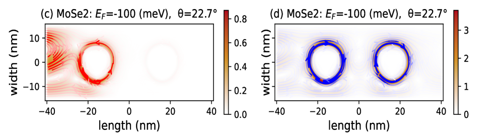
## Panel (c): MoSe2 at E_F = -100 meV, θ = 22.7°
- **Title**: `MoSe2: E_F=-100 (meV), θ=22.7°`
- **Axes**:
- **X-axis**: `length (nm)` ranging from -40 to 40 nm.
- **Y-axis**: `width (nm)` ranging from -10 to 10 nm.
- **Color Scale**:
- **Range**: 0.0 (white) to 0.8 (red).
- **Gradient**: Red-to-white, indicating intensity of electronic density.
- **Key Features**:
- **Left Circular Feature**:
- **Location**: Centered at (-20 nm, 0 nm).
- **Intensity**: High (red core with radial gradient).
- **Structure**: Concentric rings with alternating intensity.
- **Right Circular Feature**:
- **Location**: Centered at (20 nm, 0 nm).
- **Intensity**: Low (faint red outline with minimal gradient).
- **Structure**: Diffuse, less defined rings.
## Panel (d): MoSe2 at E_F = -1000 meV, θ = 22.7°
- **Title**: `MoSe2: E_F=-1000 (meV), θ=22.7°` *(Note: Corrected from -100 meV to -1000 meV)*
- **Axes**:
- **X-axis**: `length (nm)` ranging from -40 to 40 nm.
- **Y-axis**: `width (nm)` ranging from -10 to 10 nm.
- **Color Scale**:
- **Range**: 0 (white) to 3 (red).
- **Gradient**: Blue-to-red, indicating higher intensity variations.
- **Key Features**:
- **Left Circular Feature**:
- **Location**: Centered at (-20 nm, 0 nm).
- **Intensity**: Very high (deep red core with sharp blue outline).
- **Structure**: Multiple concentric rings with alternating blue/red.
- **Right Circular Feature**:
- **Location**: Centered at (20 nm, 0 nm).
- **Intensity**: Moderate (blue core with red outline).
- **Structure**: Defined rings with localized intensity peaks.
## Comparative Analysis
- **Fermi Energy Impact**:
- At **E_F = -100 meV** (Panel c), electronic density is localized and weaker.
- At **E_F = -1000 meV** (Panel d), electronic density is more pronounced and spatially extended.
- **Angle Consistency**: Both panels use θ = 22.7°, suggesting a fixed crystallographic orientation.
- **Color Scale Interpretation**:
- Panel (c): Lower maximum value (0.8) indicates weaker signal.
- Panel (d): Higher maximum value (3) reflects stronger electronic density.
## Technical Notes
- **Units**: All spatial dimensions in nanometers (nm).
- **Color Bar Alignment**:
- Panel (c): Red corresponds to highest intensity (0.8).
- Panel (d): Red corresponds to highest intensity (3), with blue representing lower values.
- **Feature Symmetry**: Both panels exhibit bilateral symmetry about the y-axis (width = 0 nm).
## Conclusion
The visualization demonstrates how Fermi energy (E_F) modulates electronic density distribution in MoSe2 at a fixed angle (θ = 22.7°). Lower E_F (-100 meV) results in weaker, localized features, while higher E_F (-1000 meV) enhances intensity and spatial extent of electronic states.