## Technical Diagram: Neural Network Hardware Accelerator Architecture
### Overview
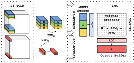
The image is a technical block diagram illustrating a hardware architecture for neural network computation, specifically showing data flow between a memory subsystem (L1 TCDM) and a compute unit (IMA). The diagram uses color-coded blocks and directional arrows to represent data movement and processing stages.
### Components/Axes
The diagram is divided into two primary sections, each enclosed by a dotted border:
**Left Section: L1 TCDM (Tightly Coupled Data Memory)**
* **Label:** "L1 TCDM" (top-left corner).
* **Components:**
* Two stacked 3D rectangular blocks, representing memory banks or data structures.
* The top stack contains three layers, colored blue, green, and yellow from top to bottom. The blue and green layers are labeled "N". The yellow layer is labeled "1".
* The bottom stack is a single white block with a red front face.
* **Data Elements:**
* Two smaller, separate 3D blocks labeled "IFM₀" (Input Feature Map 0). These are colored blue, green, and yellow, matching the top stack in L1 TCDM.
* Two smaller, separate 3D blocks labeled "OFM₀" (Output Feature Map 0). These are colored red, matching the front face of the bottom stack in L1 TCDM.
**Right Section: IMA (In-Memory Accelerator)**
* **Label:** "IMA" (top-right corner).
* **Components & Data Flow (from top to bottom):**
1. **Input Buffer:** A vertical rectangle containing three colored squares (blue, green, yellow) labeled "i".
2. **DAC (Digital-to-Analog Converter):** A vertical rectangle to the right of the Input Buffer.
3. **Weights crossbar:** A large, central dotted rectangle. Inside, the text "Weights crossbar" is written. Below it is the formula: **"Wᵀ x IFM₀ = OFM₀"**.
4. **ADC (Analog-to-Digital Converter):** A horizontal rectangle below the crossbar.
5. **Output Buffer:** A horizontal rectangle at the bottom, colored red and labeled "1".
**Data Flow Arrows & Labels:**
* **STREAM-IN:** An arrow points from the left (L1 TCDM area) into the Input Buffer of the IMA.
* **STREAM-OUT:** An arrow points from the Output Buffer of the IMA back to the left (towards the L1 TCDM area).
* **Internal Flow:** Arrows connect the components within the IMA in sequence: Input Buffer → DAC → Weights crossbar → ADC → Output Buffer.
### Detailed Analysis
* **Color Coding:** The diagram uses a consistent color scheme to trace data:
* **Blue/Green/Yellow:** Represents input data (IFM₀). This color set appears in the L1 TCDM memory stack, the separate IFM₀ blocks, and the Input Buffer of the IMA.
* **Red:** Represents output data (OFM₀). This color appears on the front of the L1 TCDM memory stack, the separate OFM₀ blocks, and the Output Buffer of the IMA.
* **Spatial Relationships:**
* The L1 TCDM is positioned on the left, acting as the data source and sink.
* The IMA is positioned on the right, acting as the computational engine.
* The "STREAM-IN" and "STREAM-OUT" arrows create a clear data loop between memory and compute.
* **Text Transcription:**
* All text is in English.
* Key labels: `L1 TCDM`, `IFM₀`, `OFM₀`, `N`, `1`, `IMA`, `Input Buffer`, `DAC`, `Weights crossbar`, `ADC`, `Output Buffer`, `STREAM-IN`, `STREAM-OUT`.
* Embedded formula: `Wᵀ x IFM₀ = OFM₀`.
### Key Observations
1. **Data Movement Pattern:** The architecture is designed for streaming data. Input feature maps (IFM₀) are streamed from memory into the accelerator, processed, and the resulting output feature maps (OFM₀) are streamed back.
2. **Compute-Memory Integration:** The core computation (`Wᵀ x IFM₀ = OFM₀`) happens within the "Weights crossbar," suggesting an analog or in-memory computing paradigm where matrix multiplication is performed directly on stored weights.
3. **Precision Indication:** The labels "N" and "1" on the memory blocks may indicate different data precisions (e.g., N-bit for activations, 1-bit for certain weights or outputs) or different data types.
4. **Component Isolation:** The diagram clearly isolates the memory subsystem (L1 TCDM) from the compute unit (IMA), highlighting a common design in specialized AI hardware.
### Interpretation
This diagram illustrates a specialized hardware accelerator, likely for convolutional neural networks (CNNs), optimized for energy-efficient matrix-vector multiplication.
* **What it demonstrates:** The system shows a complete data path for a single layer operation. Input activations (IFM₀) are fetched from a local, low-latency memory (L1 TCDM), converted to analog signals (DAC), multiplied by stored weight matrices (Wᵀ) in a crossbar array, converted back to digital (ADC), and the result (OFM₀) is written back to memory.
* **Relationships:** The L1 TCDM provides the high-bandwidth, low-latency data supply necessary to keep the compute unit (IMA) fed. The IMA's internal pipeline (Buffer → DAC → Crossbar → ADC → Buffer) is a classic representation of an analog compute-in-memory (CIM) or digital accelerator architecture.
* **Notable Design Choices:** The use of a "crossbar" strongly implies an analog CIM approach, where the weights are stored as conductance values and the multiplication is performed using Kirchhoff's laws, offering massive parallelism and energy efficiency for specific operations. The separate "STREAM-IN" and "STREAM-OUT" paths suggest a full-duplex data interface to maximize throughput. The color-coding effectively traces the lifecycle of a single data element (IFM₀) through its transformation into an output (OFM₀).