## Block Diagram: Sequential Adder Circuit
### Overview
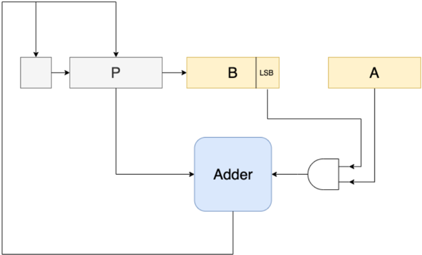
The image displays a technical block diagram of a digital logic circuit, likely representing a sequential arithmetic component such as a multiplier or accumulator. The diagram uses colored blocks, arrows, and a logic gate to illustrate data flow and control relationships between components.
### Components/Axes
The diagram consists of the following labeled components and their spatial relationships:
1. **Unlabeled Square (Top-Left):** A small, light gray square. It receives a feedback input from the bottom of the diagram and sends an output to the "P" block.
2. **Block "P" (Top-Center-Left):** A light gray rectangular block labeled "P". It receives inputs from the unlabeled square and a feedback line from the "Adder". It sends outputs to block "B" and the "Adder".
3. **Block "B" (Top-Center):** A yellow rectangular block labeled "B". It contains a sub-section labeled "LSB" (Least Significant Bit) on its right side. It receives an input from "P". Its "LSB" output connects to one input of the AND gate.
4. **Block "A" (Top-Right):** A yellow rectangular block labeled "A". It sends an output to the second input of the AND gate.
5. **AND Gate (Center-Right):** A standard logic gate symbol (white with a black outline) representing an AND operation. Its inputs come from the "LSB" of block "B" and from block "A". Its output connects to the "Adder".
6. **Adder (Center-Bottom):** A light blue, rounded rectangular block labeled "Adder". It receives inputs from block "P" and the AND gate. Its output forms a feedback loop that connects back to the unlabeled square and block "P".
**Spatial Grounding:** The legend (component labels) is integrated directly onto the blocks. The primary flow is from left to right (P -> B -> AND gate) and top to bottom (Adder output feedback). The feedback loop runs from the bottom of the Adder, up the left side of the diagram, and back into the top-left components.
### Detailed Analysis
**Component Flow and Relationships:**
* The circuit forms a closed loop, indicating sequential operation.
* The "Adder" is the central processing unit, summing two inputs.
* One input to the Adder comes directly from block "P".
* The second input to the Adder is *gated* by an AND gate. This gate only allows the value from block "A" to pass through to the Adder if the "LSB" of block "B" is active (logic high/1).
* The result from the Adder is fed back to update the state of the initial components (the unlabeled square and block "P").
**Text Transcription:**
All text is in English.
* Block Labels: "P", "B", "A", "Adder"
* Sub-component Label: "LSB" (within block "B")
### Key Observations
1. **Conditional Addition:** The core function is conditional. The value from "A" is only added to "P" when the least significant bit of "B" is 1.
2. **State Feedback:** The output of the Adder updates the input stage ("P" and the unlabeled square), suggesting this is one stage of an iterative process.
3. **Color Coding:** Components are color-coded by function: light gray for input/state registers ("P", unlabeled square), yellow for data operands ("A", "B"), and light blue for the arithmetic unit ("Adder").
4. **Architectural Pattern:** This structure is characteristic of a **shift-and-add multiplier** or a similar sequential arithmetic logic unit (ALU). In such a circuit, "B" would typically be a shift register, and its LSB controls whether the multiplicand ("A") is added to the partial product ("P") in each cycle.
### Interpretation
This diagram illustrates the fundamental data path for a single cycle of a sequential binary multiplication algorithm. The "Peircean" investigative reading reveals the underlying logic:
* **Sign (The Diagram Itself):** It is an iconic representation of a hardware process.
* **Index (The Connections):** The arrows indexically point to the cause-and-effect flow: the state of "B" directly causes the AND gate to either block or permit the flow of "A".
* **Symbol (The Function):** The AND gate symbolizes conditional logic, and the Adder symbolizes accumulation. Together, they represent the rule: "If the current bit of the multiplier (B) is 1, add the multiplicand (A) to the partial product (P)."
**What the Data Suggests:** The circuit is designed for efficiency. Instead of performing full multiplication in one complex step, it breaks it down into simpler, repeated conditional additions controlled by the bits of one operand. The feedback loop is essential for this iterative process.
**Notable Anomaly/Clarification:** The small, unlabeled square is ambiguous. It could represent a clock input, a control signal generator, or simply a junction point in the schematic. Its exact function cannot be determined from the diagram alone, which is a minor gap in the technical documentation.