## Flowchart: Digital Circuit Process Flow
### Overview
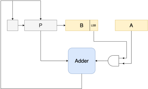
The image depicts a technical flowchart illustrating a digital circuit process involving multiple components connected via directional arrows. The system includes labeled blocks (P, B, LSB, A, Adder) and a NOT gate, with feedback loops and data flow paths. The diagram emphasizes binary logic operations and signal routing.
### Components/Axes
- **Blocks**:
- **P**: Input source (gray box).
- **B**: Intermediate processing unit (orange box).
- **LSB**: Sub-component of B (smaller orange box labeled "LSB").
- **A**: Secondary input/output unit (orange box).
- **Adder**: Central processing unit (blue box).
- **NOT Gate**: Binary logic inverter (standard logic symbol).
- **Arrows**: Indicate data flow direction between components.
- **Feedback Loops**: Two feedback paths from the Adder to B and A.
### Detailed Analysis
1. **Data Flow Paths**:
- **P → B**: Primary input from P to B.
- **B → LSB**: B routes data to its LSB sub-component.
- **B → Adder**: B feeds into the Adder.
- **A → Adder**: A feeds into the Adder.
- **Adder → NOT Gate**: Adder output is inverted.
- **NOT Gate → B**: Inverted signal feeds back into B.
- **Adder → A**: Adder output also routes to A.
2. **Component Roles**:
- **P**: Likely represents a power or primary input signal.
- **B**: Processes data, with LSB handling lower-order bits.
- **Adder**: Combines inputs from B and A, suggesting arithmetic operations.
- **NOT Gate**: Introduces binary inversion, critical for feedback control.
3. **Feedback Mechanism**:
- The Adder’s output is split into two paths:
- One path inverts the signal (via NOT) and returns to B.
- Another path routes directly to A, enabling iterative adjustments.
### Key Observations
- **Binary Logic**: The presence of a NOT gate and LSB labeling confirms binary operations.
- **Feedback Control**: The loop from Adder to B suggests error correction or stabilization.
- **Modular Design**: Separation of B into B and LSB implies hierarchical processing.
### Interpretation
This flowchart likely represents a **digital adder circuit with carry-lookahead logic** or a similar structure. The feedback loop from the Adder to B via the NOT gate indicates a control mechanism to adjust intermediate values (B) based on computation results, ensuring accuracy. The LSB sub-component suggests optimization for handling lower-order bits separately, common in high-speed arithmetic units. The dual feedback paths (to B and A) imply a system designed for iterative refinement, possibly in applications like digital signal processing or error-corrected memory systems. The modular design highlights efficiency in managing complex binary operations.