## Diagram:Integrated Circuit Layout
### Overview
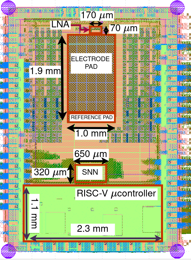
The image depicts a technical schematic of an integrated circuit (IC) layout, showcasing multiple components with precise spatial dimensions and interconnections. Key elements include an **Electrode Pad**, **Reference Pad**, **SNN (Spiking Neural Network)**, **RISC-V μcontroller**, and **LNA (Low Noise Amplifier)**. Dimensions are annotated in micrometers (μm) and millimeters (mm), with directional arrows indicating spatial relationships.
### Components/Axes
1. **Electrode Pad**:
- Dimensions: 1.9 mm (height) × 1.0 mm (width).
- Positioned centrally, labeled with a red rectangular outline.
- Connected to an **LNA** (170 μm) via a bidirectional arrow.
2. **Reference Pad**:
- Located directly above the Electrode Pad.
- Dimensions: 70 μm (width).
3. **SNN**:
- Dimensions: 650 μm (width) × 320 μm (height).
- Positioned below the Electrode Pad, outlined in red.
4. **RISC-V μcontroller**:
- Dimensions: 2.3 mm (width) × 1.1 mm (height).
- Located at the bottom of the layout, outlined in red.
5. **LNA**:
- Dimensions: 170 μm.
- Positioned above the Electrode Pad, labeled with a bidirectional arrow.
6. **BISC-V μcontroller**:
- Dimensions: 70 μm.
- Located near the top-right corner, labeled with a bidirectional arrow.
### Detailed Analysis
- **Electrode Pad**:
- Central component with a grid-like internal structure (blue and green cross-hatching).
- Connected to the LNA via a red arrow, suggesting signal input/output.
- **Reference Pad**:
- Smaller than the Electrode Pad, positioned directly above it.
- Likely serves as a calibration or grounding reference.
- **SNN**:
- Rectangular region with internal segmentation (blue and green lines).
- Positioned below the Electrode Pad, indicating signal processing flow.
- **RISC-V μcontroller**:
- Largest component at the bottom, with a green background and internal segmentation.
- Dimensions suggest it occupies the majority of the lower layout area.
- **LNA and BISC-V μcontroller**:
- Smallest components (170 μm and 70 μm, respectively).
- Positioned at the periphery, likely for signal conditioning and control.
### Key Observations
1. **Hierarchical Structure**:
- The layout follows a top-down hierarchy: LNA → Electrode Pad → SNN → RISC-V μcontroller.
- The Reference Pad acts as a secondary interface above the Electrode Pad.
2. **Spatial Efficiency**:
- Components are tightly packed, with minimal unused space.
- The RISC-V μcontroller’s large size (2.3 mm × 1.1 mm) dominates the lower region.
3. **Signal Flow**:
- Arrows indicate bidirectional communication between the LNA and Electrode Pad.
- The SNN’s position below the Electrode Pad suggests downstream processing.
### Interpretation
This layout represents a compact, optimized IC design for neural signal processing. The **Electrode Pad** serves as the primary interface for external signals, amplified by the **LNA**. The **SNN** processes these signals, while the **RISC-V μcontroller** manages computational tasks. The **Reference Pad** likely ensures signal integrity. The use of precise dimensions (e.g., 650 μm for the SNN) highlights a focus on miniaturization and efficiency. The bidirectional arrows suggest dynamic interaction between components, critical for real-time signal processing.
**Notable Trends**:
- The RISC-V μcontroller’s size implies it is the computational core.
- The LNA’s small size (170 μm) contrasts with its critical role in signal amplification.
- The Reference Pad’s proximity to the Electrode Pad suggests tight coupling for noise reduction.
**Anomalies**:
- No explicit legend is present, but color coding (red for pads, green for the μcontroller) is consistent.
- The BISC-V μcontroller’s placement near the periphery may indicate auxiliary control functions.