## Block Diagram and Specification Table: Chip Architecture Overview
### Overview
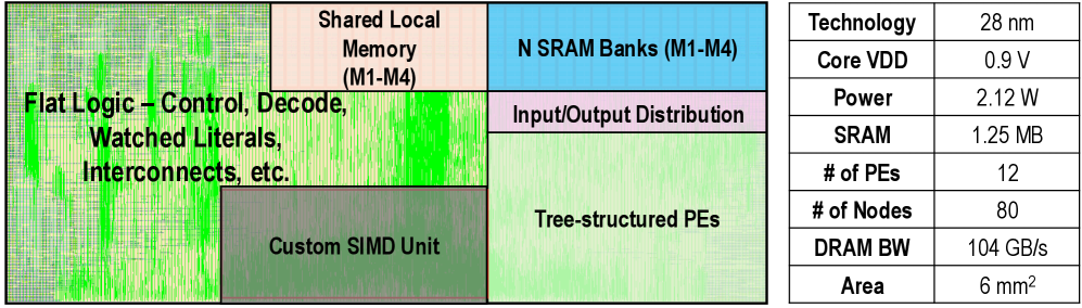
The image presents a high-level architectural floorplan of a semiconductor chip alongside a corresponding technical specification table. The diagram illustrates the functional partitioning of the chip's silicon area, while the table provides quantitative performance and physical metrics for the design.
### Components/Axes
**Diagram Components (Left Side):**
The diagram is a rectangular block layout representing the chip's functional units:
* **Left Region:** A large, textured green block labeled "Flat Logic – Control, Decode, Watched Literals, Interconnects, etc."
* **Top-Center Region:** A light peach-colored block labeled "Shared Local Memory (M1-M4)."
* **Top-Right Region:** A light blue block labeled "N SRAM Banks (M1-M4)."
* **Middle-Right Region:** A light purple/pink block labeled "Input/Output Distribution."
* **Bottom-Center Region:** A dark grey/brown block labeled "Custom SIMD Unit."
* **Bottom-Right Region:** A light green block labeled "Tree-structured PEs."
**Table Components (Right Side):**
A two-column table listing technical specifications:
* **Column 1 (Parameter):** Technology, Core VDD, Power, SRAM, # of PEs, # of Nodes, DRAM BW, Area.
* **Column 2 (Value):** 28 nm, 0.9 V, 2.12 W, 1.25 MB, 12, 80, 104 GB/s, 6 mm².
### Detailed Analysis
**Table Data Extraction:**
| Parameter | Value |
| :--- | :--- |
| Technology | 28 nm |
| Core VDD | 0.9 V |
| Power | 2.12 W |
| SRAM | 1.25 MB |
| # of PEs | 12 |
| # of Nodes | 80 |
| DRAM BW | 104 GB/s |
| Area | 6 mm² |
**Diagram Layout Analysis:**
* **Control/Logic:** The "Flat Logic" block occupies the largest portion of the chip area, indicating that the control, decoding, and interconnect logic (specifically for "Watched Literals") is the primary consumer of silicon real estate.
* **Memory Hierarchy:** The memory is split into two distinct types: "Shared Local Memory" and "N SRAM Banks," suggesting a tiered memory architecture to support the processing units.
* **Processing Units:** The chip utilizes a heterogeneous processing approach, combining a "Custom SIMD Unit" with "Tree-structured PEs" (Processing Elements).
### Key Observations
* **Specialized Architecture:** The inclusion of "Watched Literals" in the logic block is a highly specific indicator. This terminology is standard in Boolean Satisfiability (SAT) solver algorithms. This suggests the chip is a domain-specific accelerator designed for SAT solving or similar constraint-satisfaction problems.
* **Compact Design:** The total area is 6 mm², which is quite small for a chip containing 12 PEs and 80 nodes, indicating a high-density, efficient design.
* **Power Efficiency:** A power consumption of 2.12 W at 0.9 V is relatively low, consistent with a specialized accelerator rather than a general-purpose processor.
* **Memory Bandwidth:** The DRAM bandwidth of 104 GB/s is significant for a chip of this size, suggesting the architecture is designed to handle high-throughput data movement between the memory and the processing elements.
### Interpretation
The data suggests this is a **domain-specific hardware accelerator** optimized for SAT solving.
* **Why it matters:** General-purpose CPUs are often inefficient at the specific logic required for SAT solving (which involves checking large sets of boolean clauses). By implementing "Watched Literals" directly in the "Flat Logic" and utilizing "Tree-structured PEs," this architecture likely achieves massive parallelism and speedups compared to software-based solvers.
* **Structural Relationships:** The "Flat Logic" acts as the central nervous system, likely managing the state of the SAT clauses. The "Custom SIMD Unit" and "Tree-structured PEs" likely perform the actual evaluation of these clauses in parallel. The memory blocks (SRAM and Shared Local Memory) serve as the high-speed cache for the clause database, minimizing the need to access external DRAM, though the high DRAM bandwidth (104 GB/s) indicates that the chip is prepared to handle large problem instances that exceed on-chip memory capacity.