\n
## Diagram: Chip Floorplan and Specifications
### Overview
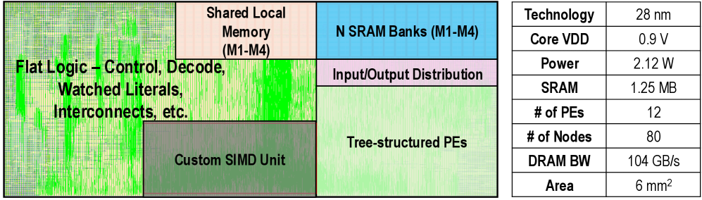
The image presents a diagram illustrating the floorplan of a chip, divided into functional blocks, alongside a table listing key specifications of the chip. The floorplan visually represents the allocation of different components within the chip's area. The table provides quantitative data about the chip's technology, power consumption, memory, and processing elements.
### Components/Axes
The diagram is divided into several rectangular blocks, each labeled with its function. The blocks are:
* **Flat Logic – Control, Decode, Watched Literals, Interconnects, etc.** (Light Green)
* **Shared Local Memory (M1-M4)** (Blue)
* **N SRAM Banks (M1-M4)** (Light Blue)
* **Input/Output Distribution** (Orange)
* **Custom SIMD Unit** (Dark Grey)
* **Tree-structured PEs** (Green)
The table on the right side lists the following specifications:
* **Technology**
* **Core VDD**
* **Power**
* **SRAM**
* **# of PEs**
* **# of Nodes**
* **DRAM BW**
* **Area**
### Detailed Analysis or Content Details
The diagram shows a partitioning of the chip area. The largest portion is occupied by the "Flat Logic" block, followed by the "Tree-structured PEs" block. The "Shared Local Memory" and "N SRAM Banks" blocks occupy significant portions as well. The "Input/Output Distribution" and "Custom SIMD Unit" blocks are smaller in size.
The table provides the following data:
* **Technology:** 28 nm
* **Core VDD:** 0.9 V
* **Power:** 2.12 W
* **SRAM:** 1.25 MB
* **# of PEs:** 12
* **# of Nodes:** 80
* **DRAM BW:** 104 GB/s
* **Area:** 6 mm²
### Key Observations
The "Flat Logic" block occupies the largest area, suggesting that control and decoding logic are significant components of this chip. The chip utilizes SRAM for local memory, with a capacity of 1.25 MB. The chip has 12 Processing Elements (PEs) and 80 nodes. The DRAM bandwidth is 104 GB/s, indicating a relatively high memory access rate. The chip's area is 6 mm².
### Interpretation
The diagram and table together describe a chip designed for parallel processing, likely a SIMD (Single Instruction, Multiple Data) architecture, as indicated by the "Custom SIMD Unit" and "Tree-structured PEs". The large "Flat Logic" area suggests a complex control structure. The 28nm technology node indicates a mature manufacturing process. The specifications suggest a balance between processing power (12 PEs, 104 GB/s DRAM BW) and power consumption (2.12 W). The chip is likely designed for applications requiring significant computational throughput with moderate power constraints. The SRAM banks and shared local memory suggest an emphasis on fast data access for the PEs. The chip's architecture appears to prioritize efficient data flow and parallel execution.