\n
## Technical Diagram: Chip Architecture Block Diagram and Specifications
### Overview
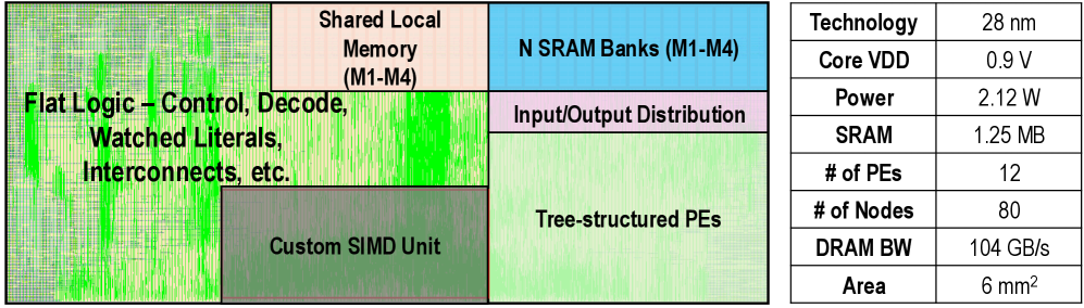
The image presents a two-part technical document: a color-coded block diagram illustrating the internal architecture of a semiconductor chip (likely a processor or accelerator) on the left, and a corresponding specifications table on the right. The diagram uses labeled rectangular regions to denote major functional units and their spatial relationships on the die.
### Components/Axes
**Diagram Components (Left Side):**
The diagram is divided into several colored blocks with the following labels and approximate positions:
1. **Flat Logic – Control, Decode, Watched Literals, Interconnects, etc.** (Large, light green region on the left side, spanning top to bottom).
2. **Custom SIMD Unit** (Darker green rectangle, positioned in the lower-left quadrant, overlapping the "Flat Logic" region).
3. **Shared Local Memory (M1-M4)** (Light peach rectangle, positioned in the top-center).
4. **N SRAM Banks (M1-M4)** (Light blue rectangle, positioned in the top-right corner).
5. **Input/Output Distribution** (Light purple rectangle, positioned directly below the "N SRAM Banks" block).
6. **Tree-structured PEs** (Light green rectangle, positioned in the bottom-right quadrant, below the "Input/Output Distribution" block).
**Specifications Table (Right Side):**
| Specification | Value |
|---------------|-------|
| Technology | 28 nm |
| Core VDD | 0.9 V |
| Power | 2.12 W |
| SRAM | 1.25 MB |
| # of PEs | 12 |
| # of Nodes | 80 |
| DRAM BW | 104 GB/s |
| Area | 6 mm² |
### Detailed Analysis
**Diagram Layout and Relationships:**
* The "Flat Logic" block appears to be the central control and routing fabric, occupying the largest area on the left.
* The "Custom SIMD Unit" is embedded within or adjacent to the "Flat Logic" area, suggesting it is tightly integrated with the control logic.
* Memory hierarchy is shown on the top and right: "Shared Local Memory" and "N SRAM Banks" are placed at the top, indicating a high-bandwidth local storage layer.
* The "Input/Output Distribution" block sits between the SRAM banks and the processing elements, likely managing data flow.
* The "Tree-structured PEs" (Processing Elements) are located at the bottom-right, receiving data from the I/O distribution network. The label "Tree-structured" implies a hierarchical interconnect topology among the PEs.
**Table Data:**
The table provides concrete technical parameters for the chip:
* Fabrication process: 28 nanometer technology.
* Operating voltage (Core VDD): 0.9 Volts.
* Power consumption: 2.12 Watts.
* On-chip SRAM capacity: 1.25 Megabytes.
* Number of Processing Elements (PEs): 12.
* Number of Nodes: 80 (This could refer to cores, clusters, or another hierarchical unit within the PEs).
* External memory bandwidth (DRAM BW): 104 Gigabytes per second.
* Physical die area: 6 square millimeters.
### Key Observations
1. **Architecture Type:** The combination of a "Custom SIMD Unit," "Tree-structured PEs," and significant on-chip SRAM (1.25 MB) strongly suggests this is a specialized accelerator chip, potentially for signal processing, machine learning inference, or high-performance computing tasks.
2. **Memory-Centric Design:** The prominent placement and labeling of multiple memory banks ("Shared Local Memory," "N SRAM Banks") highlight a design focused on high-bandwidth, low-latency data access to feed the processing elements.
3. **Integration:** The "Flat Logic" block encompassing control, decode, and interconnects indicates a highly integrated system-on-chip (SoC) design where control and data path are closely coupled.
4. **Efficiency Metrics:** The specifications point to a power-efficient design (2.12 W) for its performance class, built on a mature 28nm process node. The area (6 mm²) is relatively small, suggesting a cost-effective or embedded application.
### Interpretation
This diagram and table collectively describe a specialized parallel processing chip. The architecture is optimized for data-parallel workloads, as evidenced by the SIMD (Single Instruction, Multiple Data) unit and the array of Processing Elements. The "Tree-structured" interconnect for the PEs suggests a design that balances communication bandwidth and latency, possibly for algorithms requiring reduction operations or hierarchical data sharing.
The high DRAM bandwidth (104 GB/s) relative to the small die area indicates the chip is designed to work on large datasets that reside in external memory, streaming them efficiently through the on-chip SRAM hierarchy to the compute units. The 12 PEs and 80 nodes imply a many-core or clustered architecture where each PE may contain multiple simpler processing nodes.
In essence, this is a technical blueprint for a domain-specific accelerator, prioritizing parallel computation, efficient memory access, and integration, likely targeting applications in embedded systems, networking, or edge computing where performance-per-watt and area are critical constraints.