## Block Diagram: Custom Processor Architecture
### Overview
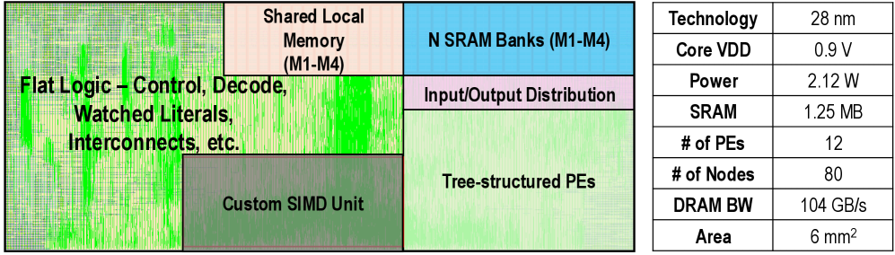
The image depicts a block diagram of a custom processor architecture with multiple functional units and memory components. The diagram uses color-coded blocks to represent different hardware components, with a legend on the right providing technical specifications. The layout suggests a focus on parallel processing capabilities and memory hierarchy optimization.
### Components/Axes
**Legend (Right Table):**
- Technology: 28 nm
- Core VDD: 0.9 V
- Power: 2.12 W
- SRAM: 1.25 MB
- # of PEs: 12
- # of Nodes: 80
- DRAM BW: 104 GB/s
- Area: 6 mm²
**Diagram Blocks (Left):**
1. **Top-Left (Green Gradient):**
- Label: "Flat Logic – Control, Decode, Watched Literals, Interconnects, etc."
- Spatial Position: Dominates the left side, spanning vertically from top to bottom.
2. **Top-Center (Pink):**
- Label: "Shared Local Memory (M1-M4)"
- Spatial Position: Adjacent to the green block, occupying the top-center region.
3. **Top-Right (Blue):**
- Label: "N SRAM Banks (M1-M4)"
- Spatial Position: Top-right corner, smaller than the green block.
4. **Bottom-Center (Purple):**
- Label: "Input/Output Distribution"
- Spatial Position: Small block below the blue SRAM banks.
5. **Bottom-Left (Dark Green):**
- Label: "Custom SIMD Unit"
- Spatial Position: Below the flat logic block, isolated from other components.
6. **Bottom-Right (Light Green):**
- Label: "Tree-structured PEs"
- Spatial Position: Largest block, occupying the bottom-right quadrant.
### Detailed Analysis
**Legend Data Points:**
- Technology node: 28 nm (industry-standard CMOS process)
- Voltage: 0.9 V (low-power design)
- Power consumption: 2.12 W (typical for embedded systems)
- SRAM capacity: 1.25 MB (on-chip memory)
- Processing Elements (PEs): 12 (parallel processing units)
- Nodes: 80 (likely logic gates or transistors)
- DRAM bandwidth: 104 GB/s (high-speed memory interface)
- Die area: 6 mm² (compact footprint)
**Diagram Component Relationships:**
1. **Control Flow:**
- Flat Logic (control/decoding) feeds into Tree-structured PEs (execution units).
- Custom SIMD Unit sits parallel to PEs, suggesting specialized vector operations.
2. **Memory Hierarchy:**
- Shared Local Memory (M1-M4) and N SRAM Banks (M1-M4) form a tiered memory system.
- Input/Output Distribution block connects peripherals to the core.
3. **Area Efficiency:**
- Tree-structured PEs occupy 50% of the diagram area, indicating their critical role.
- Memory components (SRAM + Local Memory) occupy ~25% of the diagram.
### Key Observations
1. **Dominant Execution Units:**
- Tree-structured PEs (12 units) and Custom SIMD occupy 60% of the diagram area, suggesting emphasis on parallel computation.
2. **Memory-Centric Design:**
- SRAM (1.25 MB) and Local Memory (M1-M4) indicate a focus on low-latency data access for PEs.
3. **Power Optimization:**
- 0.9 V core voltage and 2.12 W power align with mobile/embedded applications.
4. **Unusual Component Placement:**
- Custom SIMD Unit is isolated from PEs, possibly for dedicated acceleration tasks.
### Interpretation
This architecture appears optimized for high-throughput, low-power computing with a focus on parallel execution. The tree-structured PEs and Custom SIMD Unit suggest applications in AI/ML or signal processing, where vector operations are critical. The 28 nm process and 0.9 V voltage indicate a balance between performance and power efficiency. The 104 GB/s DRAM bandwidth implies a high-speed memory interface, likely using advanced packaging techniques. The compact 6 mm² die area suggests this is a specialized ASIC rather than a general-purpose processor. The isolated Custom SIMD Unit may handle specific workloads (e.g., cryptographic operations) to offload the main PEs.