# Visual Description
<details>
<summary>Image 1 Details</summary>

### Visual Description
## Logo: "PoS" Stylized Text Logo
### Overview
The image displays a stylized text logo consisting of the letters "P", "o", and "S". The design uses a two-tone green color scheme on a plain white background. The logo appears to be a brand or company identifier, possibly for an organization, product, or service abbreviated as "PoS".
### Components/Axes
* **Primary Text Elements:** Three letters forming the acronym "PoS".
* **Color Scheme:**
* **Dark Green:** Used for the uppercase letters "P" and "S".
* **Light Green:** Used for the lowercase letter "o".
* **Background:** Solid white.
* **Font Style:** A serif typeface with distinct, classic styling. The letters have pronounced serifs (the small lines attached to the end of a stroke in a letter).
### Detailed Analysis
* **Letter "P":** An uppercase "P" in dark green. It is positioned on the left side of the composition. The vertical stem is on the left, with the curved bowl extending to the right.
* **Letter "o":** A lowercase "o" in light green. It is positioned centrally, nestled between the "P" and the "S". It is slightly smaller in height than the uppercase letters and overlaps the lower right curve of the "P" and the lower left curve of the "S".
* **Letter "S":** An uppercase "S" in dark green. It is positioned on the right side of the composition. The letter has a classic, balanced serpentine curve.
* **Spatial Arrangement:** The letters are tightly kerned (spaced closely together). The central "o" acts as a visual bridge, connecting the two larger, darker outer letters. The overall composition is horizontally aligned and centered within the white rectangular frame.
### Key Observations
* **Color Contrast:** The use of two distinct shades of green creates visual hierarchy and interest. The darker green provides weight and definition to the outer letters, while the lighter green makes the central "o" stand out as a unique element.
* **Typographic Style:** The serif font choice conveys a sense of tradition, reliability, or formality.
* **Integration:** The overlapping of the "o" with the "P" and "S" creates a unified, cohesive mark rather than three separate letters.
### Interpretation
This logo is a compact, visually balanced representation of the acronym "PoS". The design choices suggest a brand identity that aims to appear established (serif font) yet approachable or innovative (the playful, integrated use of color and overlap for the "o"). The color green often symbolizes growth, harmony, safety, or nature, which may hint at the organization's field or values. Without additional context, the specific meaning of "PoS" remains ambiguous, but the logo itself is designed for clear recognition and memorability. The technical execution is clean, with high contrast ensuring legibility at various sizes.
</details>
## QCD on the Cell Broadband Engine
F. Belletti a , G. Bilardi b , M. Drochner c , N. Eicker d , e , Z. Fodor e , f , D. Hierl g , H. Kaldass h , i ,
- T. Lippert d , e , T. Maurer g , N. Meyer ∗ g , A. Nobile j , k , D. Pleiter i , A. Schäfer g ,
- F. Schifano a , H. Simma i , k , S. Solbrig g , T. Streuer l , R. Tripiccione a , T. Wettig g
Email: nils.meyer@physik.uni-regensburg.de
a Department of Physics, University of Ferrara, 44100 Ferrara, Italy
b Department of Information Engineering, University of Padova, 35131 Padova, Italy
c ZEL, Research Center Jülich, 52425 Jülich, Germany
d ZAM, Research Center Jülich, 52425 Jülich, Germany
e Department of Physics, University of Wuppertal, 42119 Wuppertal, Germany
f Institute for Theoretical Physics, Eotvos University, Budapest, Pazmany 1, H-1117, Hungary
g Department of Physics, University of Regensburg, 93040 Regensburg, Germany
h Arab Academy of Science and Technology, P.O. Box 2033, Cairo, Egypt
i Deutsches Elektronen-Synchrotron DESY, 15738 Zeuthen, Germany
j European Centre for Theoretical Studies ECT ∗ , 13050 Villazzano, Italy
k Department of Physics, University of Milano - Bicocca, 20126 Milano, Italy
l Department of Physics and Astronomy, University of Kentucky, Lexington, KY 40506-0055, USA
We evaluate IBM's Enhanced Cell Broadband Engine (BE) as a possible building block of a new generation of lattice QCD machines. The Enhanced Cell BE will provide full support of doubleprecision floating-point arithmetics, including IEEE-compliant rounding. We have developed a performance model and applied it to relevant lattice QCD kernels. The performance estimates are supported by micro- and application-benchmarks that have been obtained on currently available Cell BE-based computers, such as IBM QS20 blades and PlayStation 3. The results are encouraging and show that this processor is an interesting option for lattice QCD applications. For a massively parallel machine on the basis of the Cell BE, an application-optimized network needs to be developed.
The XXV International Symposium on Lattice Field Theory
July 30 - August 4 2007
Regensburg, Germany
∗ Speaker.
<details>
<summary>Image 2 Details</summary>

### Visual Description
## [Text Logo/Header]: Proceedings of Science
### Overview
The image displays a text-based logo or header, likely for an academic journal, conference proceedings, or scientific publication. The design is simple, featuring white text on a solid green background.
### Components/Axes
* **Background:** A solid, uniform green color fills the entire frame.
* **Text:** The words "PROCEEDINGS OF SCIENCE" are displayed in a white, serif typeface (similar to Times New Roman or Garamond). The text is arranged in three lines, centered horizontally and vertically within the image.
* Line 1: "PROCEEDINGS"
* Line 2: "OF"
* Line 3: "SCIENCE"
* **Layout:** The text is the sole focal point. There are no other graphical elements, borders, or icons present.
### Detailed Analysis
* **Text Transcription:**
* **Primary Text (English):** "PROCEEDINGS OF SCIENCE"
* **Visual Characteristics:**
* **Font:** Serif font with distinct strokes and terminals.
* **Color:** High-contrast white text on a medium-green background.
* **Alignment:** Perfectly centered, both horizontally and vertically.
* **Case:** All letters are in uppercase.
### Key Observations
* The design is minimalist and professional, prioritizing legibility and a formal tone.
* The color scheme (green and white) is clean and often associated with themes of growth, nature, and clarity, which can be relevant to scientific fields.
* There is no additional metadata, such as a volume number, date, or publisher logo, visible in this specific crop.
### Interpretation
This image serves as a title banner or masthead. Its primary function is to identify the publication or series. The formal serif font and centered layout convey authority and tradition, which are common values in academic publishing. The lack of any data, charts, or complex imagery indicates this is purely an identifying header, not a content-bearing figure. The phrase "Proceedings of Science" suggests the document contains compiled papers, presentations, or reports from a scientific conference or symposium.
</details>
http://pos.sissa.it/
## 1. Introduction
The initial target platform of the Cell BE was the PlayStation 3, but the processor is currently also under investigation for scientific purposes [1, 2]. It delivers extremely high floating-point (FP) performance, memory and I/O bandwidths at an outstanding price-performance ratio and low power consumption.
We have investigated the Cell BE as a potential compute node of a next-generation lattice QCD machine. Although the double precision (DP) performance of the current version of the Cell BE is rather poor, the announced Enhanced Cell BE version (2008) will have a DP performance of ∼ 100 GFlop/s and also implement IEEE-compliant rounding. We have developed a performance model of a relevant lattice QCD kernel on the Enhanced Cell BE and investigated several possible data layouts. The applicability of our model is supported by a variety of benchmarks performed on commercially available platforms. We also discuss requirements for a network coprocessor that would enable scalable parallel computing using the Cell BE.
## 2. The Cell Broadband Engine
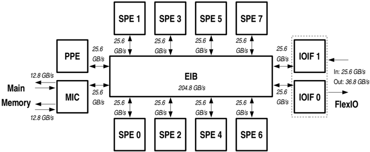
An introduction to the processor can be found in Ref. [3], and a schematic diagram is shown in Fig. 1. The architecture is described in detail in Ref. [4], and we only give a brief overview here.
The Cell BE comprises one PowerPC Processor Element (PPE) and 8 Synergistic Processor Elements (SPE). In the following we will assume that performance-critical kernels are executed on the SPEs and that the PPE will execute control threads. Therefore, we only consider the performance of the SPEs. Each of the dual-issue, in-order SPEs runs a single thread and has a dedicated 256 kB on-chip memory (local store = LS) which is accessible by direct memory access (DMA) or by local load/store operations to/from the 128 general purpose 128-bit registers. An SPE can execute two instructions per cycle, performing up to 8 single precision (SP) operations. Thus, the aggregate SP peak performance of all 8 SPEs on a single Cell BE is 204.8 GFlop/s at 3.2 GHz. 1
Figure 1: Main functional units of the Cell BE (see Ref. [4] for details). Bandwidth values are given for a 3.2 GHz system clock.
<details>
<summary>Image 3 Details</summary>
### Visual Description
## Block Diagram: Cell Broadband Engine Architecture
### Overview
This image is a technical block diagram illustrating the high-level architecture and data pathways of the Cell Broadband Engine processor. It shows the central interconnect, processing elements, memory interface, and I/O interfaces, with specific data transfer rates labeled for each connection.
### Components/Axes
The diagram is organized around a central rectangular block labeled **EIB** (Element Interconnect Bus). Surrounding this central bus are several other functional blocks connected via bidirectional arrows.
**Central Component:**
* **EIB**: Labeled with a peak bandwidth of **204.8 GB/s**.
**Processing Elements (Top and Bottom Rows):**
* **SPE 1, SPE 3, SPE 5, SPE 7**: Located in a row above the EIB.
* **SPE 0, SPE 2, SPE 4, SPE 6**: Located in a row below the EIB.
* Each of these eight **SPE** (Synergistic Processing Element) blocks connects to the EIB with a labeled bandwidth of **25.6 GB/s**.
**Control and Memory Interface (Left Side):**
* **PPE** (Power Processing Element): Positioned to the left of the EIB, connected with a bandwidth of **25.6 GB/s**.
* **MIC** (Memory Interface Controller): Positioned below the PPE and to the left of the EIB. It connects to the EIB with a bandwidth of **25.6 GB/s**.
* **Main Memory**: Represented by text and arrows to the left of the MIC. The connection between Main Memory and the MIC is labeled with a bandwidth of **12.8 GB/s** (in both directions).
**I/O Interfaces (Right Side):**
* **IOIF 1** and **IOIF 0**: Two blocks enclosed within a dashed rectangle on the right side of the EIB.
* Each **IOIF** connects to the EIB with a bandwidth of **25.6 GB/s**.
* **IOIF 1** has an external input arrow labeled **In: 25.6 GB/s**.
* **IOIF 0** has an external output arrow labeled **Out: 36.8 GB/s** and is also connected to a label **FlexIO**.
### Detailed Analysis
**Spatial Layout and Connections:**
* The **EIB** is the central hub, with all other components connected directly to it.
* The eight **SPEs** are symmetrically placed, four above and four below the EIB.
* The **PPE** and **MIC** are stacked vertically on the left, forming the control and memory subsystem.
* The **IOIF** blocks are stacked vertically on the right, forming the I/O subsystem, with the dashed box suggesting they are part of a unified I/O interface group.
**Data Flow and Bandwidths:**
* **Internal Peak Bandwidth:** The EIB itself is rated for **204.8 GB/s**.
* **Component-to-EIB Links:** All direct connections from the EIB to the PPE, MIC, SPEs, and IOIFs are rated at **25.6 GB/s** each.
* **External Memory Link:** The path from the MIC to Main Memory has a lower bandwidth of **12.8 GB/s**.
* **External I/O Links:** The diagram specifies asymmetric external I/O bandwidths: **25.6 GB/s** for input (to IOIF 1) and **36.8 GB/s** for output (from IOIF 0).
### Key Observations
1. **Symmetry and Scalability:** The uniform connection bandwidth (25.6 GB/s) for all processing elements (SPEs) and the PPE to the EIB suggests a balanced, scalable design for parallel processing.
2. **Bandwidth Hierarchy:** There is a clear hierarchy: the internal EIB bandwidth (204.8 GB/s) is significantly higher than any single component link (25.6 GB/s), which in turn is higher than the main memory link (12.8 GB/s). This indicates a design optimized for high internal data movement.
3. **I/O Asymmetry:** The specified output bandwidth (36.8 GB/s) is higher than the input bandwidth (25.6 GB/s), which may reflect a design bias towards data processing and output (e.g., for graphics or scientific computation results).
4. **Component Roles:** The diagram clearly segregates functions: computation (SPEs, PPE), memory control (MIC), interconnection (EIB), and I/O (IOIFs).
### Interpretation
This diagram depicts a high-performance, heterogeneous multi-core processor architecture, specifically the Cell Broadband Engine used in systems like the PlayStation 3 and some supercomputers.
* **Architectural Philosophy:** The design emphasizes high-bandwidth, low-latency communication between specialized processing units via a central, high-speed bus (EIB). The PPE handles general-purpose control, while the eight SPEs are designed for intensive, parallel numerical computations.
* **Performance Implications:** The bottleneck for overall system performance is likely not the internal interconnect (EIB) but the external links, particularly the **12.8 GB/s** connection to main memory. This is a classic "memory wall" scenario where processor capability outpaces memory bandwidth.
* **Data Flow Inference:** The architecture is built for a "streaming" data model. Data flows in from I/O (e.g., 25.6 GB/s), is processed in parallel by the SPEs using data staged in their local stores (not shown), and results are streamed out (e.g., at 36.8 GB/s). The high EIB bandwidth facilitates the rapid shuffling of data between these units.
* **Design Intent:** The explicit labeling of bandwidths underscores that this architecture is engineered for predictable, high-throughput data processing, making it suitable for media processing, scientific simulation, and other bandwidth-intensive workloads. The asymmetry in I/O suggests it's optimized for workloads that generate more output data than input, or where output latency is critical.
</details>
1 Available systems use clock frequencies of 2.8 or 3.2 GHz. In our estimates we assume 3.2 GHz.
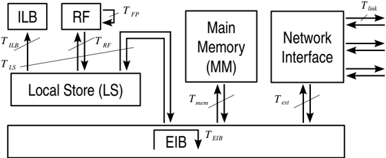
Figure 2: Data-flow paths and associated execution times Ti . For simplicity, only a single SPE is shown.
<details>
<summary>Image 4 Details</summary>
### Visual Description
## Block Diagram: Processor/System-on-Chip (SoC) Architecture
### Overview
The image is a technical block diagram illustrating the high-level architecture and data/control flow of a processing system, likely a specialized processor or system-on-chip (SoC). It shows the interconnection between core computational units, memory hierarchy, and external interfaces via a central bus.
### Components/Axes
The diagram consists of several labeled rectangular blocks representing functional units, connected by arrows indicating data or control flow. Timing or latency parameters are labeled alongside these connections.
**Main Components (Blocks):**
1. **ILB** (Top-left)
2. **RF** (Top-left, to the right of ILB)
3. **Local Store (LS)** (Center-left, below ILB and RF)
4. **Main Memory (MM)** (Center)
5. **Network Interface** (Center-right)
6. **EIB** (Bottom, spanning the width of the diagram)
**Connections and Timing Labels:**
* **ILB to LS:** A single upward arrow labeled `T_ILB`.
* **LS to ILB:** A single downward arrow labeled `T_LS`.
* **RF to LS:** A double-headed arrow (bidirectional) labeled `T_RF`.
* **RF to MM:** A double-headed arrow (bidirectional) labeled `T_FP`.
* **LS to EIB:** A thick, downward-pointing arrow (indicating a bus or wide data path).
* **MM to EIB:** A double-headed arrow labeled `T_mem`.
* **Network Interface to EIB:** A double-headed arrow labeled `T_ext`.
* **EIB Internal:** A downward arrow within the EIB block labeled `T_EIB`.
* **Network Interface External:** Multiple horizontal arrows pointing to/from the right edge of the diagram, labeled `T_link`.
### Detailed Analysis
**Spatial Layout and Flow:**
* **Top-Left Region:** Contains the **ILB** and **RF** units, which are closely coupled with the **Local Store (LS)**. This suggests a local, high-speed processing cluster.
* **Central Region:** Houses the **Main Memory (MM)** and **Network Interface**, acting as bridges to larger storage and external systems.
* **Bottom Region:** The **EIB** (likely standing for *External Interface Bus* or *Element Interconnect Bus*) serves as the central communication backbone, connecting all major components.
* **Data Flow:** The arrows depict a clear hierarchy. The ILB/RF/LS cluster processes data locally. For larger datasets or external communication, data moves via the EIB to/from the Main Memory or Network Interface.
**Component Relationships:**
* The **Local Store (LS)** acts as a scratchpad or cache, directly serving the ILB and RF.
* The **RF** (Register File) has a direct, bidirectional link to **Main Memory (MM)**, labeled `T_FP`. This could indicate a path for floating-point operations or direct memory access (DMA) by the register file.
* The **Network Interface** manages all external communication (`T_link`), funneling data through the EIB (`T_ext`) to the rest of the system.
### Key Observations
1. **Centralized Interconnect:** The EIB is the single point of connection for the Local Store, Main Memory, and Network Interface, making it a critical potential bottleneck.
2. **Asymmetric Local Access:** The ILB has a dedicated, likely read-only, path from the LS (`T_ILB`), while the RF has a full bidirectional path (`T_RF`). This suggests the ILB might be an instruction buffer or loader.
3. **Direct RF-Memory Path:** The `T_FP` connection between RF and MM is notable, bypassing the LS and EIB for certain operations, which could be optimized for performance.
4. **Timing-Centric Design:** Every major data path is annotated with a timing parameter (`T_...`), emphasizing that latency and synchronization are critical design considerations for this architecture.
### Interpretation
This diagram represents a **performance-optimized, memory-centric computing architecture**. The design prioritizes low-latency access for local processing (ILB/RF/LS cluster) while providing scalable paths to larger memory and external networks.
* **What it demonstrates:** The system is built for tasks requiring high-bandwidth, low-latency local computation (e.g., signal processing, scientific computing) with the ability to handle large datasets (via MM) and communicate with other systems (via Network Interface).
* **Relationships:** The hierarchy is clear: Fast, local resources (LS) feed specialized processors (ILB, RF). The EIB orchestrates data movement between this fast layer and the slower, larger-capacity or external layers (MM, Network).
* **Notable Design Choice:** The direct `T_FP` link between the Register File and Main Memory is a significant architectural feature. It implies the system may support operations that stream data directly from main memory into registers for processing, minimizing intermediate storage overhead. This is common in high-performance computing (HPC) or graphics processing unit (GPU) designs.
* **Potential Bottleneck:** The EIB's role as the sole conduit for MM and Network traffic means its bandwidth and latency (`T_EIB`) will fundamentally limit the system's overall throughput for non-local operations.
</details>
The current version of the Cell BE has an on-chip memory controller supporting dual-channel access to the Rambus XDR main memory (MM), which will be replaced by DDR2 for the Enhanced Cell BE. The configurable I/O interface supports a coherent as well as a non-coherent protocol on the Rambus FlexIO channels. 2 Internally, all units of the Cell BE are connected to the coherent element interconnect bus (EIB) by DMA controllers.
## 3. Performance model
To theoretically investigate the performance of the Cell BE, we use a refined performance model along the lines of Refs. [5, 6]. Our abstract model of the hardware architecture considers two classes of devices: ( i ) Storage devices : These store data and/or instructions (e.g., registers or LS) and are characterized by their storage size. ( ii ) Processing devices : These act on data (e.g., FP units) or transfer data/instructions from one storage device to another (e.g., DMA controllers, buses, etc.) and are characterized by their bandwidths β i and startup latencies λ i .
An application algorithm, implemented on a specific machine, can be broken down into different computational micro-tasks which are performed by the processing devices of the machine model described above. The execution time Ti of each task i is estimated by a linear ansatz
$$T _ { i } = I _ { 1 } ( B _ { i } + \sigma ( a _ { i } ) ,$$
where I i quantifies the information exchange, i.e., the processed data in bytes.
Assuming that all tasks are running concurrently at maximal throughput and that all dependencies (and latencies) are hidden by suitable scheduling, the total execution time is
$$\frac { T _ { i } ^ { 2 } - m T _ { i } } { p }$$
We denote by T peak the minimal compute time for the FP operations of an application that could be achieved with an ideal implementation (i.e., saturating the peak FP throughput of the machine, assuming also perfect matching between its instruction set architecture and the computation). The floating point efficiency ε FP for a given application is then defined as ε FP = T peak / T exe .
In our analysis, we have estimated the execution times Ti for data processing and transport along all data paths indicated in Fig. 2, in particular:
2 In- and outbound bandwidths will be symmetric on the Enhanced Cell BE, namely 25.6 GB/s each.
- floating-point operations, T FP
- load/store operations between register file (RF) and LS, T RF
- off-chip memory access, T mem
- internal communications between SPEs on the same Cell BE, T int
- external communications between different Cell BEs, T ext
- transfers via the EIB (memory access, internal and external communications), T EIB
Unless stated otherwise, all hardware parameters β i are taken from the Cell BE manuals [4].
## 4. Linear algebra kernels
As a simple application of our performance model and to verify our methodology, we analyzed various linear algebra computations. As an example, we discuss here only a caxpy operation: c · ψ + ψ ′ with complex c and complex spin-color vectors ψ and ψ ′ . If the vectors are stored in main memory (MM), the memory bandwidth dominates the execution time, T exe ≈ T mem, and limits the FP performance of the caxpy kernel to ε FP ≤ 4 . 1%. On the other hand, if the vectors are held in the LS, arithmetic operations and LS access are almost balanced ( T peak / T LS = 2 / 3). In this case, a more precise estimate of T FP also takes into account constraints from the instruction set architecture of the Cell BE for complex arithmetics and yields a theoretical limit of ε FP ≤ 50%.
We have verified the predictions of our theoretical model by benchmarks on several hardware systems (Sony PlayStation 3, IBM QS20 Blade Server and Mercury Cell Accelerator Board). In both cases (data in MM and LS) the theoretical time estimates are well reproduced by the measurements. Careful optimization of arithmetic operations 3 is required only in the case in which all data are kept in the LS (or, in general, if T exe ≈ T FP).
## 5. Lattice QCD kernel
The Wilson-Dirac operator is the kernel most relevant for the performance of lattice QCD codes. We considered the computation of the 4-d hopping term
$$\sum _ { \mu = 1 } ^ { 4 } \{ U _ { x , \mu } ( 1 + y _ { p } ) w _ { x + \mu } + U _ { t - \mu }$$
where x = ( x 1 , x 2 , x 3 , x 4 ) is a 4-tuple of space-time coordinates labeling the lattice sites, ψ ′ x and ψ x are complex spin-color vectors assigned to the lattice site x , and Ux , µ is an SU(3) color matrix assigned to the link from site x in direction ˆ µ .
The computation of Eq. (5.1) on a single lattice site amounts to 1320 floating-point operations. 4 On the Enhanced Cell BE this yields T peak = 330 cycles per site (in DP). However, the implementation of Eq. (5.1) requires at least 840 multiply-add operations and T FP ≥ 420 cycles per lattice site to execute. Thus, any implementation of Eq. (5.1) cannot exceed 78% of the peak performance of the Cell BE.
3 We implemented our benchmarks of arithmetic operations in single precision. However, the theoretical analysis presented here refers to double precision on the Enhanced Cell BE.
4 We do not include sign flips and complex conjugation in the FLOP counting.
The time spent on possible remote communications and on load/store operations for the operands (9 × 12 + 8 × 9 complex numbers) of the hopping term (5.1) strongly depends on the details of the lattice data layout. We assign to each Cell BE a local lattice with V Cell = L 1 × L 2 × L 3 × L 4 sites, and the 8 SPEs are logically arranged as s 1 × s 2 × s 3 × s 4 = 8. Thus, each single SPE holds a subvolume of V SPE =( L 1 / s 1 ) × ( L 2 / s 2 ) × ( L 3 / s 3 ) × ( L 4 / s 4 ) = V Cell / 8 sites. Each SPE on average has A int neighboring sites on other SPEs within and A ext neighboring sites outside a Cell BE.
We consider a communication network with the topology of a 3-d torus. We assume that the 6 inbound and the 6 outbound links can simultaneously transfer data, each at a bandwidth of β link = 1 GB/s, and that a bidirectional bandwidth of β ext = 6 GB/s is available between each Cell BE and the network. This could be realized by attaching an efficient network controller via the FlexIO interface. We have investigated different strategies for the lattice and data layout: Either all data are kept in the on-chip local store of the SPEs, or the data reside in off-chip main memory.
## Data in on-chip memory (LS)
We require that all data for a compute task can be kept in the LS of the SPEs. Since loading of all data into the LS at startup is time-consuming, the compute task should comprise a sizable fraction of the application code. In QCD this can be achieved, e.g., by implementing an entire iterative solver with repeated computation of Eq. (5.1). Apart from data, the LS must also hold a minimal program kernel, the run-time environment, and intermediate results. Therefore, the storage requirements strongly constrain the local lattice volumes V SPE and V Cell .
The storage requirement of a spinor field ψ x is 24 real words (192 Byte in double precision) per site, while a gauge field Ux , µ needs 18 words (144 Byte) per link. Assuming that for a solver we need storage corresponding to 8 spinors and 3 × 4 links per site, the subvolume carried by a single SPE cannot be larger than about V SPE = 79 lattice sites. Moreover, one lattice dimension, say the 4-direction, must be distributed locally within the same Cell BE across the SPEs (logically arranged as an 1 3 × 8 grid). Then, L 4 corresponds to a global lattice extension and, as a pessimistic assumption, may be as large as L 4 = 64. This yields a very asymmetric local lattice 5 with V Cell = 2 3 × 64 and V SPE = 2 3 × 8.
## Data in off-chip main memory (MM)
When all data are stored in MM, there are no a-priori restrictions on V Cell . On the other hand, we need to minimize redundant memory accesses to reload the operands of Eq. (5.1) into the LS when sweeping through the lattice. To also allow for concurrent FP computation and data transfers (to/from MM or remote SPEs), we consider a multiple buffering scheme. 6 A possible implementation of such a scheme is to compute the hopping term (5.1) on a 3-d slice of the local lattice and then move the slice along the 4-direction. Each SPE stores all sites along the 4-direction, and the SPEs are logically arranged as a 2 3 × 1 grid to minimize internal and to balance external communications between SPEs. If the U - and ψ -fields associated with all sites of three 3-d slices can be kept in the LS at the same time, all operands in Eq. (5.1) are available in the LS. This optimization requirement again constrains the local lattice size, now to V Cell ≈ 800 × L 4 sites.
5 When distributed over 4096 Cell BEs, this corresponds to a global lattice size of 32 3 × 64.
6 In multiple buffering schemes several buffers are used in an alternating fashion to either process or load/store data. This requires additional storage (here in the LS) but allows for concurrent computation and data transfer.
Table 1: Comparison of the theoretical time estimates Ti (in 1000 SPE cycles) for some micro-tasks arising in the computation of Eq. (5.1) for different lattice data layouts: keeping data either in the on-chip LS (left part) or in the off-chip MM (right part). The first rows indicate the corresponding number of neighbor sites A int and A ext. Estimated efficiencies, ε FP = T peak / max i Ti , are shown in the last row.
| data in on-chip LS | data in on-chip LS | data in off-chipMM | data in off-chipMM | data in off-chipMM | data in off-chipMM |
|----------------------|----------------------|----------------------|----------------------|----------------------|----------------------|
| V Cell | 2 × 2 × 2 × 64 | L 1 × L 2 × L 3 | 8 × 8 × 8 | 4 × 4 × 4 | 2 × 2 × 2 |
| A int | 16 | A int / L 4 | 48 | 12 | 3 |
| A ext | 192 | A ext / L 4 | 48 | 12 | 3 |
| T peak | 21 | T peak / L 4 | 21 | 2.6 | 0.33 |
| T FP | 27 | T FP / L 4 | 27 | 3.4 | 0.42 |
| T RF | 12 | T RF / L 4 | 12 | 1.5 | 0.19 |
| T mem | - | T mem / L 4 | 61 | 7.7 | 0.96 |
| T int | 2 | T int / L 4 | 5 | 1.2 | 0.29 |
| T ext | 79 | T ext / L 4 | 20 | 4.9 | 1.23 |
| T EIB | 20 | T EIB / L 4 | 40 | 6.1 | 1.06 |
| ε FP | 27% | ε FP | 34% | 34% | 27% |
The predicted execution times for some of the micro-tasks considered in our model are given in Table 1 for both data layouts and for reasonable choices of the local lattice size. If all data are kept in the LS, the theoretical efficiency of about 27% is limited by the communication bandwidth ( T exe ≈ T ext ). This is also the limiting factor for the smallest local lattice with data kept in MM, while for larger local lattices the memory bandwidth becomes the limiting factor ( T exe ≈ T mem).
Wehave performed hardware benchmarks with the same memory access pattern as (5.1), using the above multiple buffering scheme for data from MM. We found that the execution times were at most 20% higher than the theoretical predictions for T mem.
## 6. Performance model and benchmarks for DMA transfers
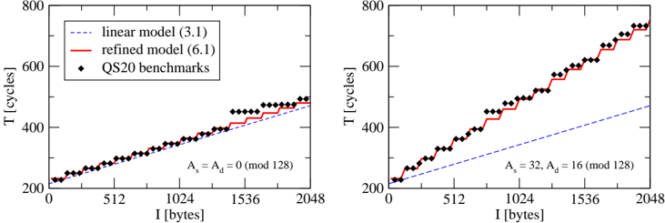
DMA transfers determine T mem, T int, and T ext, and their optimization is crucial to exploit the Cell BE performance. Our analysis of detailed micro-benchmarks, e.g., for LS-to-LS transfers, shows that the linear model Eq. (3.1) does not accurately describe the execution time of DMA operations with arbitrary size I and address alignment. We refined our model to take into account the fragmentation of data transfers, as well as source and destination addresses, As and Ad , of the buffers:
$$\frac { T _ { D M A } ( I , A s , A d ) = \lambda ^ { 0 } } { p } + \lambda ^ { a } \cdot N _ { a } ( I , A s , A d ) + N _ { b } ( I , A s ) \cdot \frac { 1 2 8 t + \lambda ^ { a } \cdot N _ { a } ( I , A s , A d ) + N _ { b } ( I , A s ) } { p }$$
Each LS-to-LS DMA transfer has a latency of λ 0 ≈ 200 cycles (from startup and wait for completion). The DMA controllers fragment all transfers into Nb 128-byte blocks aligned at LS lines (and corresponding to single EIB transactions). When δ A = As -Ad is a multiple of 128, the source LS lines can be directly mapped onto the destination LS lines. Then, we have Na = 0, and the effective bandwidth β eff = I / ( T DMA -λ 0 ) is approximately the peak value. Otherwise, if the alignments do not match ( δ A not a multiple of 128), an additional latency of λ a ≈ 16 cycles is introduced for each
Figure 3: Execution time of LS-to-LS copy operations as a function of the transfer size. In the left panel source and destination addresses are aligned, while in the right panel they are misaligned. Filled diamonds show the measured values on an IBM QS20 system. Dashed and full lines correspond to the theoretical prediction from Eq. (3.1) and Eq. (6.1), respectively.
<details>
<summary>Image 5 Details</summary>
### Visual Description
## [Line Charts]: Performance Comparison of Linear vs. Refined Models Under Different Alignment Conditions
### Overview
The image contains two side-by-side line charts comparing the performance (in CPU cycles) of a "linear model" and a "refined model" against actual "QS20 benchmarks" as a function of input size `I` in bytes. The charts illustrate how model accuracy changes under two different memory alignment conditions.
### Components/Axes
* **Chart Type:** Two 2D line plots with scatter points.
* **X-Axis (Both Charts):** Label: `I [bytes]`. Scale: Linear, from 0 to 2048. Major tick marks at 0, 512, 1024, 1536, 2048.
* **Y-Axis (Both Charts):** Label: `T [cycles]`. Scale: Linear, from 200 to 800. Major tick marks at 200, 400, 600, 800.
* **Legend (Located in top-left of the left chart, applies to both):**
* Blue dashed line: `linear model (3.1)`
* Red solid line: `refined model (6.1)`
* Black diamond marker: `QS20 benchmarks`
* **Chart-Specific Titles (Centered below each plot):**
* Left Chart: `A_s = A_d = 0 (mod 128)`
* Right Chart: `A_s = 32, A_d = 16 (mod 128)`
### Detailed Analysis
**Left Chart (`A_s = A_d = 0 (mod 128)`):**
* **Trend Verification:**
* **Linear Model (Blue Dashed):** Shows a steady, approximately linear upward trend from ~220 cycles at I=0 to ~480 cycles at I=2048.
* **Refined Model (Red Solid):** Exhibits a step-function pattern. It increases in discrete jumps, with plateaus between jumps. It closely follows the benchmark data.
* **QS20 Benchmarks (Black Diamonds):** Also follows a clear step-function pattern, very similar to the refined model.
* **Data Points & Values (Approximate):**
* At I=0: All series start near 220 cycles.
* First major plateau for benchmarks/refined model: ~300 cycles for I from ~256 to ~768.
* Second major plateau: ~400 cycles for I from ~1024 to ~1536.
* Final value at I=2048: Benchmarks and refined model are at ~500 cycles, while the linear model is slightly lower at ~480 cycles.
**Right Chart (`A_s = 32, A_d = 16 (mod 128)`):**
* **Trend Verification:**
* **Linear Model (Blue Dashed):** Shows a linear upward trend, but with a much shallower slope than in the left chart. It starts near 220 cycles and ends at approximately 460 cycles at I=2048.
* **Refined Model (Red Solid):** Shows a steeper, more continuous upward trend with smaller, more frequent steps compared to the left chart.
* **QS20 Benchmarks (Black Diamonds):** Follows a very similar steep, stepped upward trend as the refined model.
* **Data Points & Values (Approximate):**
* At I=0: All series start near 220 cycles.
* The refined model and benchmarks diverge significantly upward from the linear model early on.
* At I=1024: Benchmarks/refined model are at ~550 cycles, while the linear model is at ~350 cycles.
* Final value at I=2048: Benchmarks and refined model reach approximately 750 cycles, while the linear model is far lower at ~460 cycles.
### Key Observations
1. **Model Accuracy:** The "refined model (6.1)" is a significantly better predictor of the actual "QS20 benchmarks" than the "linear model (3.1)" in both alignment scenarios. The red line and black diamonds are nearly coincident.
2. **Impact of Alignment:** The alignment parameters (`A_s`, `A_d`) dramatically affect performance. The non-zero alignment condition (right chart) results in a much steeper increase in cycles (T) as input size (I) grows, compared to the zero-alignment condition (left chart).
3. **Step-Function Behavior:** The benchmark data exhibits a clear step-function characteristic, suggesting performance changes at specific input size thresholds (likely related to cache lines or memory block sizes of 128 bytes, as hinted by the `mod 128` in the titles).
4. **Linear Model Limitation:** The linear model fails to capture the step-function nature and, more critically, severely underestimates performance cost under the non-zero alignment condition (right chart).
### Interpretation
This data demonstrates the critical importance of modeling low-level hardware effects, such as memory alignment, when predicting computational performance. The "linear model" likely represents a simplified theoretical analysis that assumes uniform cost per byte. In contrast, the "refined model" incorporates the real-world, non-linear effects of memory access patterns, which are heavily influenced by alignment (`A_s`, `A_d`) and manifest as step-functions due to cache line boundaries (128-byte blocks).
The stark difference between the two charts shows that misaligned memory accesses (`A_s=32, A_d=16`) incur a much higher and more rapidly growing cycle cost as the data size increases. The refined model's ability to accurately track the benchmark data in both scenarios validates its underlying assumptions and makes it a reliable tool for performance estimation and optimization in systems where memory alignment is a factor. The charts argue that ignoring these effects (as the linear model does) leads to grossly inaccurate performance predictions.
</details>
transferred 128-byte block, reducing β eff by about a factor of two. Fig. 3 illustrates how clearly these effects are observed in our benchmarks and how accurately they are described by Eq. (6.1).
## 7. Conclusion and outlook
Our performance model and hardware benchmarks indicate that the Enhanced Cell BE is a promising option for lattice QCD. We expect that a sustained performance above 20% can be obtained on large machines. A refined theoretical analysis, e.g., taking into account latencies, and benchmarks with complete application codes are desirable to confirm our estimate. Strategies to optimize codes and data layout can be studied rather easily, but require some effort to implement.
Since currently there is no suitable southbridge for the Cell BE to enable scalable parallel computing, we plan to develop a network coprocessor that allows us to connect Cell BE nodes in a 3-d torus with nearest-neighbor links. This network coprocessor should provide a bidirectional bandwidth of 1 GB/s per link for a total bidirectional network bandwidth of 6 GB/s and perform remote LS-to-LS copy operations with a latency of order 1 µ s. Pending funding approval, this development will be pursued in collaboration with the IBM Development Lab in Böblingen, Germany.
## References
- [1] S. Williams et al., The Potential of the Cell Processor for Scientific Computing , Proceedings of the 3rd conference on Computing frontiers (2006) 9, DOI 10.1145/1128022.1128027
- [2] A. Nakamura, Development of QCD-code on a Cell machine , PoS(LAT2007)040
- [3] H.P. Hofstee et al., Cell Broadband Engine technology and systems , IBM J. Res. & Dev. 51 (2007) 501
- [4] http://www.ibm.com/developerworks/power/cell
- [5] G. Bilardi et al., The Potential of On-Chip Multiprocessing for QCD Machines , Springer Lecture Notes in Computer Science 3769 (2005) 386
- [6] N. Meyer, A. Nobile and H. Simma, Performance Estimates on Cell , internal reports and talk at Cell Cluster Meeting, Jülich 2007, http://www.fz-juelich.de/zam/datapool/cell/Lattice\_QCD\_on\_Cell.pdf