## FPGA-Based CNN Inference Accelerator Synthesized from Multi-Threaded C Software
†
Samsung Semiconductor Inc., San Jose, CA, USA
Jin Hee Kim, Brett Grady, Ruolong Lian, John Brothers , Jason H. Anderson Dept. of Electrical and Computer Engineering, University of Toronto, Toronto, ON, Canada †
Email:
{ kimjin14, bgrady, janders } @ece.utoronto.ca
Abstract -A deep-learning inference accelerator is synthesized from a C -language software program parallelized with Pthreads. The software implementation uses the well-known producer/consumer model with parallel threads interconnected by FIFO queues. The LegUp high-level synthesis (HLS) [1] tool synthesizes threads into parallel FPGA hardware, translating software parallelism into spatial parallelism. A complete system is generated where convolution, pooling and padding are realized in the synthesized accelerator, with remaining tasks executing on an embedded ARM processor. The accelerator incorporates reduced precision, and a novel approach for zero-weight-skipping in convolution. On a mid-sized Intel Arria 10 SoC FPGA, peak performance on VGG-16 is 138 effective GOPS.
## I. INTRODUCTION
State-of-the-art accuracy results in image recognition, language translation, image-caption generation, and many other tasks are being achieved with deep convolutional neural networks (CNNs) (e.g. [2], [3], [4]). CNN training is very compute intensive, requiring hours, days or weeks of time using state-of-the-art graphics processing units (GPUs). Applying a trained CNN to a recognition task, inference , can involve billions of operations. Hardware acceleration is particularly desirable for inference, as training is typically done once offline, whereas inference with a trained network is applied repeatedly. Moreover, there is increased emphasis on performing CNN inference in an embedded-computing context (e.g. mobile handsets, self-driving cars), where low-power and low latency are important metrics. In this paper, we focus on acceleration of CNN inference.
CNN inference has been accelerated with GPUs, custom ASICs, and recently, field-programmable gate arrays (FPGAs). At present, it is unclear which IC media will ultimately prevail as best for CNN inference acceleration. However, the speed at which CNN research is evolving, as well as recent research on low-precision CNNs [5] bodes well for FPGA technology. With FPGAs, the accelerator architecture and its datapath widths can be precisely tailored to the target CNN, whereas an ASIC or GPU are necessarily over-engineered with fixed-sized datapaths to handle a broad set of precisions. Moreover, the reconfigurability of FPGAs permits an accelerator design to be adapted to incorporate new research findings as they arise, for example, the ability to achieve high recognition accuracy with 2-bit precision [6]. Lastly, high-level synthesis (HLS) is a relatively mature design methodology for FPGAs [7], permitting a software specification of the accelerator to be synthesized into hardware. HLS lowers NRE costs by allowing design and debugging to proceed at a higher level of abstraction vs. manual RTL design.
We apply HLS and use an FPGA to realize a CNN inference accelerator. The accelerator is described in C and synthesized with the LegUp HLS framework [1]. A unique aspect of LegUp is its ability to synthesize software parallelized with the Pthreads standard into parallel hardware [8]. We leverage the Pthreads synthesis to exploit spatial parallelism on the FPGA. Specifically, we specify the accelerator in software using the producer/consumer parallelization idiom, well known to software engineers. 20 parallel software threads are synthesized by LegUp HLS into streaming hardware comprising compute kernels interconnected by FIFO queues.
The inference accelerator performs key compute-intensive operations: convolution, subsampling (pooling), and padding. Software executing on an embedded on-die ARM processor performs remaining operations to provide a complete end-toend embedded solution. The accelerator architecture incorporates novel features for tiling, data-reuse, and zero-weightskipping, as many CNNs can be pruned without significant loss of accuracy [9]. The accelerator's computations are realized in reduced precision, specifically 8-bit magnitude + sign format. We demonstrate our accelerator on the VGG-16 CNN for image recognition (ImageNet database). Our contributions are as follows:
- An FPGA-based CNN accelerator synthesized from multi-threaded (Pthreads) C software. The software behavior closely resembles the synthesized hardware, easing design and debugging by allowing it to proceed in software.
- Generation and exploration of accelerator architectural variants via software/constraint changes alone.
- Analysis of the efficiency of the HLS implementation, in terms of cycles spent, compared to the theoretical minimum for the architecture.
- A novel architecture for zero-skipping; use of reducedprecision arithmetic.
- A complete end-to-end solution for CNN inference, integrated with Caffe for network training.
- 138 GOPS peak effective performance implementing the VGG-16 CNN for image recognition on a midsized Arria 10 SoC SX660 20 n m FPGA.
## II. BACKGROUND
## A. LegUp High-Level Synthesis
The Pthreads synthesis flow of LegUp HLS is used to synthesize parallel software threads into parallel hardware. The multi-threaded software is written using the producer/consumer paradigm, where threads represent computational kernels and communicate with one another through FIFO queues [8]. Producer threads deposit computed partial results into output queues, which are then retrieved by concurrently running consumer threads, which perform further processing. Note that a given thread can be both a producer and a consumer, receiving inputs from FIFO queues, computing on those inputs, and depositing results to output FIFO queues. The support in LegUp HLS for hardware synthesis of the producer/consumer parallel model is well-aligned with the computational and communication requirements of deep CNN inference.
FIFO queues that interconnect kernels are realized with a LegUp HLS-provided LEGUP\_PTHREAD\_FIFO structure and API, and can be created with user-provided lengths and bitwidths. To illustrate the coding style (used heavily throughout our implementation), the example below shows a function with one input queue, inQ , and one output queue, outQ . The function body contains an infinite while loop that reads an input, inputData from inQ , performs computation to produce output outData , and deposits into outQ . pthread\_fifo\_read and pthread\_fifo\_write are API functions to read-from and write-to queues, respectively. The while loop is pipelined in hardware by LegUp to realize a streaming kernel that accepts new input each clock cycle.
```
void prodCons(LEGUP_PTHREAD_FIFO *inQ, LEGUP_PTHREAD_FIFO *outQ) {
...
while (1) {
inputData = pthread_fifo_read(inQ);
outputData = compute(inputData);
pthread_fifo_write(outQ, outputData);
}
}
```
## B. VGG-16 CNN
The VGG-16 CNN [3] is used as the test vehicle for our accelerator. The input to the CNN is a 224 × 224 RGB image drawn from the 1000-category ImageNet database. The image is first passed through 13 convolution layers interspersed with occasional max-pooling layers, ending with 3 fully connected layers. All convolutional filters are 3 × 3 pixels in dimension. Before each convolutional layer, the input feature maps are padded with 0 s around the perimeter. Max-pooling is done for 2 × 2 regions with a stride of 2. ReLU activation is applied in all cases ( y = max (0 , x ) , where x is the neuron output). The VGG-16 network has over 130M parameters and the reader is referred to [3] for complete details.
## III. ARCHITECTURE
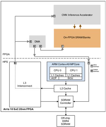
Fig. 1 depicts the system-on-chip (SoC) architecture, consisting of a Cortex A9 hard processor system (HPS), accelerator, DMA controller, and SRAM banks within the Arria 10 FPGA fabric. The on-FPGA banks are backed by offchip DDR4 RAM. The components are connected to one another using Avalon, Intel's on-chip memory mapped bus interface (discussed below). Bus masters are designated with M in the figure; slaves are designated with S. The processor issues instructions to the DMA and accelerator by writing to the memory mapped address (connected through the L3 interconnect). DMA transfers between the off-chip DRAM and FPGA are realized by a direct connection from the DMA unit to the SDRAM controller.
## A. Accelerator Architecture
We first introduce the data representation, as it is necessary to understand the zero-skipping approach. Feature maps are organized into tiles of 4 × 4 values, as shown on the left side of Fig. 2. The center of the figure shows a 16 × 16 feature map, comprising 4 × 4 tiles. These tiles are stored
X0
X4
X8
X1
X5
X9
X2
X6
XA
X3
X7
XB
XC
XD
XE
XF
!"#$%&'%()(%*+#,$-
Fig. 1. System architecture.
<details>
<summary>Image 1 Details</summary>
### Visual Description
## Diagram: CNN Inference Accelerator Architecture
### Overview
The diagram illustrates a heterogeneous computing system architecture for CNN inference acceleration. It integrates FPGA, ARM Cortex-A9 MPCore, DDR4 SDRAM, and On-FPGA SRAM Banks, with data flow managed via L3 Interconnect, DMA, and master/slave interfaces.
### Components/Axes
- **Key Components**:
- **FPGA**: Arria 10 SoC 20nm FPGA (left side).
- **HPS**: Connected to FPGA via L3 Interconnect.
- **ARM Cortex-A9 MPCore**: Central block with dual CPUs (CPU0, CPU1), L1/L2 caches, ACP, SCU, and SDRAM Controller.
- **Off-chip DDR4 SDRAM**: Connected to SDRAM Controller.
- **CNN Inference Accelerator**: Top-right block, linked to On-FPGA SRAM Banks.
- **On-FPGA SRAM Banks**: Orange block, directly connected to CNN Inference Accelerator.
- **DMA**: Gray block, bridges FPGA and ARM Cortex-A9 MPCore.
- **Data Flow**:
- Arrows indicate bidirectional communication (e.g., FPGA ↔ HPS, ARM ↔ DDR4 SDRAM).
- Master/slave interfaces (labeled "M" and "S") define communication roles.
### Detailed Analysis
- **FPGA and HPS**:
- FPGA (Arria 10 SoC 20nm) connects to HPS via L3 Interconnect.
- DMA mediates data transfer between FPGA and ARM Cortex-A9 MPCore.
- **ARM Cortex-A9 MPCore**:
- Dual CPUs (CPU0, CPU1) with shared L1 caches.
- ACP (Advanced Communication Peripheral) and SCU (System Control Unit) manage system-level tasks.
- L2 Cache sits between CPUs and SDRAM Controller.
- **Memory Hierarchy**:
- Off-chip DDR4 SDRAM is the primary memory, controlled by the SDRAM Controller.
- On-FPGA SRAM Banks provide low-latency access for the CNN Inference Accelerator.
- **CNN Inference Accelerator**:
- Directly connected to On-FPGA SRAM Banks, suggesting optimized data throughput for inference tasks.
### Key Observations
1. **Hierarchical Design**:
- FPGA and HPS handle peripheral/data acquisition, while ARM Cortex-A9 MPCore manages general computation.
- CNN Inference Accelerator offloads specialized tasks to On-FPGA SRAM for speed.
2. **Memory Optimization**:
- On-FPGA SRAM Banks reduce latency for the CNN accelerator compared to off-chip DDR4 SDRAM.
- L3 Interconnect and DMA enable efficient data sharing between FPGA and ARM cores.
3. **Interface Roles**:
- Master/slave labels ("M" and "S") clarify communication directionality (e.g., FPGA as master to HPS).
### Interpretation
This architecture prioritizes **performance isolation** and **data locality**:
- The CNN Inference Accelerator leverages On-FPGA SRAM for rapid access, critical for low-latency inference.
- ARM Cortex-A9 MPCore handles general-purpose tasks, offloading compute-heavy CNN work to the FPGA.
- The use of DMA and L3 Interconnect minimizes CPU overhead for data transfers, improving scalability.
The design reflects a **coarse-grained parallelism** approach, where specialized hardware (FPGA accelerator) and general-purpose cores (ARM) collaborate via optimized memory and interconnects. The absence of explicit numerical values suggests a focus on architectural relationships rather than quantitative benchmarks.
</details>
-/0"2$
X0
X4
X8
XC
X0
X4
X8
XC
X0
X4
X8
XC
X0
X4
X8
XC
X3
X7
XB
XF
X3
X7
XB
XF
X3
X7
XB
XF
X3
X7
XB
XF
X0
X4
X8
XC
X0
X4
X8
XC
X0
X4
X8
XC
X0
X4
X8
XC
X1
X5
X9
XD
X1
X5
X9
XD
X1
X5
X9
XD
X1
X5
X9
XD
X2
X6
XA
XE
X2
X6
XA
XE
X2
X6
XA
XE
X2
X6
XA
XE
X3
X7
XB
XF
X3
X7
XB
XF
X3
X7
XB
XF
X3
X7
XB
XF
X2
X6
XA
XE
X2
X6
XA
XE
X2
X6
XA
XE
X2
X6
XA
X3
X7
XB
XF
X3
X7
XB
XF
X3
X7
XB
XF
X3
X7
XB
X0
X4
X8
XC
X0
X4
X8
XC
X0
X4
X8
XC
X0
X4
X8
X1
X5
X9
XD
X1
X5
X9
XD
X1
X5
X9
XD
X1
X5
X9
X2
X6
XA
XE
X2
X6
XA
XE
X2
X6
XA
XE
X2
X6
XA
X3
X0
X1
X7
XB
XF
X3
X7
XB
XF
X3
X7
XB
XF
X3
X7
XB
XF
X4
X8
XC
X0
X4
X8
XC
X0
X4
X8
XC
X0
X4
X8
X5
X9
XD
X1
X5
X9
XD
X1
X5
X9
XD
X1
X5
X9
XC
XD
XE
XF
XC
XD
XE
X1
X5
X9
XD
X1
X5
X9
XD
X1
X5
X9
XD
X1
X5
X9
XD
X2
X6
XA
XE
X2
X6
XA
XE
X2
X6
XA
XE
X2
X6
XA
XE
.$+/,0$%1+2
Fig. 2. Tile concept, feature map, stripe, data layout.
in memory in row-major order, depicted on the right, where colors of tiles correspond to those in the center image. Fig. 2 also introduces the notion of a stripe , which is a region of tiles spanning the entire width of a feature map. Striping is used to subdivide large convolutional layers into smaller ones that can be accommodated in on-chip memory.
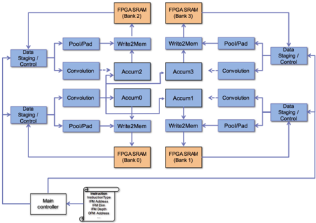
A block diagram of the accelerator is shown in Fig. 3. Four banks of on-FPGA SRAM are shown in orange. An entire tile of data (16 values) can be read from an SRAM bank in a single cycle. The on-FPGA SRAM banks are dual-port: reads are from port A; writes are to port B. The primary computing
Fig. 3. Accelerator block diagram (each blue module is synthesized from a software thread to hardware).
<details>
<summary>Image 2 Details</summary>
### Visual Description
## Block Diagram: FPGA-Based Data Processing Pipeline
### Overview
The diagram illustrates a modular data processing architecture for an FPGA (Field-Programmable Gate Array) system. It depicts data flow between memory banks, processing units, and control logic, emphasizing parallelism and iterative computation. The system includes four FPGA SRAM banks (0-3), data staging/control modules, pooling/padding units, memory write operations, accumulation stages, and convolution layers.
### Components/Axes
- **FPGA SRAM Banks**: Four memory banks labeled "FPGA SRAM (Bank 0)" to "FPGA SRAM (Bank 3)" in orange.
- **Data Staging/Control**: Blue blocks on the left and right edges, acting as input/output interfaces.
- **Pool/Pad**: Blue blocks connected to Data Staging/Control and Convolution units.
- **Write2Mem**: Blue blocks linking Pool/Pad to Accumulation stages.
- **Accumulation Stages**: Four blocks labeled "Accum0" to "Accum3" in the center.
- **Convolution**: Blue blocks connected to Accumulation stages and Pool/Pad.
- **Main Controller**: A white block at the bottom-left, sending instructions to FPGA SRAM banks.
### Detailed Analysis
1. **Data Flow Path**:
- **Input**: Data enters via "Data Staging/Control" on the left, flows through Pool/Pad, then Write2Mem to Accumulation stages (Accum0-3).
- **Processing**: Accumulation stages feed into Convolution units, which loop back to Pool/Pad and Data Staging/Control.
- **Output**: Processed data exits via "Data Staging/Control" on the right.
2. **FPGA SRAM Banks**:
- Banks 0-3 are arranged in a 2x2 grid, with Bank 0 at the bottom-left and Bank 3 at the top-right.
- Each bank receives instructions from the Main Controller, specifying parameters like `InstructionType`, `IFM Address`, `IFM Dim`, `IFM Depth`, and `OFM Address`.
3. **Control Logic**:
- The Main Controller orchestrates operations by sending structured instructions to FPGA SRAM banks.
- Feedback loops from Convolution to Pool/Pad and Data Staging/Control suggest iterative or recurrent processing.
### Key Observations
- **Parallelism**: Four SRAM banks enable concurrent data storage/retrieval.
- **Modular Design**: Components are decoupled, allowing scalability (e.g., adding more Accumulation/Convolution stages).
- **Feedback Mechanism**: Convolution outputs re-enter the pipeline, indicating support for recurrent neural networks or iterative algorithms.
### Interpretation
This architecture is optimized for high-throughput, parallel data processing, likely for machine learning workloads (e.g., convolutional neural networks). The Main Controller’s instruction set implies programmability, allowing customization of data dimensions (`IFM Dim`, `IFM Depth`) and output formats (`OFM Address`). The feedback loop suggests the system can handle temporal or spatial dependencies in data, critical for tasks like video processing or recurrent networks. The use of FPGA SRAM banks highlights a focus on low-latency, hardware-accelerated computation.
</details>
!"!"!
3&451+6&0%/"#$%1$1&07%#+7&,/
units are shown in blue - each is a software thread in the software implementation. Observe that there are 4 instances of 5 different compute units: 20 units (threads) in total. Edges in the figure represent multiple FIFO queues for communication of data/control between the units; queues are not shown for clarity.
The high-level behavior is as follows: The datastaging/control units receive an instruction from the ARM processor to perform convolution, padding, or max-pooling. We do not focus on fully connected layers, since it is essentially matrix multiplication and most CNN computational work comprises convolution. Although the padding and subsampling operations can be performed by a processor fairly efficiently, in most CNNs, they are tightly interleaved with convolution operations. Supporting them in hardware minimizes memory traffic between the FPGA and HPS.
For a convolution instruction, four tiles from different output feature maps (OFMs) are computed simultaneously. The four concurrently computed OFM tiles are at the same x/y location. Each data-staging/control unit loads a subset of input feature maps (IFMs) from an on-FPGA SRAM bank, as well as corresponding filter weight data from four filters. On each clock cycle weights and IFM data are injected into the convolution units. Each convolution unit performs 64 multiply operations each clock cycle, thus the entire accelerator performs 256 multiplication operations per cycle. Products from the convolution units are sent to the accumulator units (center of the figure). Each accumulator unit is responsible for maintaining the values of one tile (16 values) in an OFM. In the figure, for clarity, some edges between convolution units and accumulator units are omitted. When an OFM tile is completed, it is sent to the write-to-memory unit and written to an on-FPGA SRAM bank.
For a padding or max-pooling instruction, the datastaging/control units send IFM data and instructions to the pool/pad units, capable of performing any style of padding/max-pooling, described below. Pooled/padded tiles are then forwarded to the write-to-memory units and written to SRAM banks. Padding/pooling of four OFM tiles is done concurrently.
## B. Convolution and Zero-Weight Skipping
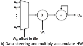
OFMs are computed on a tile-by-tile basis to completion without any intermediate swap-out to off-chip memory in an output-stationary manner. This style allows us to keep a fixed datapath width and not compromise accuracy by rounding partial sums. The convolution unit contains a computational sub-module that multiplies one weight per clock cycle to 16 IFM values and accumulates the resulting 16 products to the corresponding 16 OFM values in an OFM tile being computed.
Fig. 4(a) shows an OFM tile (lower right), a weight tile (upper right), and four contiguous IFM tiles. For this example, assume that the upper-left IFM tile is x/y aligned with the OFM tile being computed and that the filter dimensions are smaller than 4 × 4 (the tile size). In a given clock cycle, a weight in the weight tile is selected and multiplied by 16 IFM values. The example illustrates, with a dotted rectangle, the region of 16 IFM values with which the weight W 5 is multiplied. Observe that the intra-tile x/y offset of W 5 defines the region of IFM values which with it is multiplied. This produces 16 products: W 5 · A 5 , W 5 · A 6 . . . W 5 · D 0 . The products are accumulated to the corresponding OFM values: O 0 , O 1 , . . . , O F , respectively.
| A 0 A 4 A 8 | A 1 3 5 6 7 B | A 2 A 0 B 1 B 2 B 3 4 |
|---------------|-----------------------|-------------------------|
| | A A A B B 5 B 6 | B 7 |
| | A 9 A A A B B B A | 8 B 9 B B |
| A C | A D A E A F B B E | C B D B F |
| C 0 | C 1 C 2 C 3 D D 2 | 0 D 1 D 3 |
| C 4 | C 5 C 6 C 7 D D 6 | 4 D 5 D 7 |
| C 8 | C 9 C A C B D 8 D 9 D | A D B |
| C C | C D C E C F D D D D E | C D F |
)(&*+%$%&'(
| W 0 | W 1 | W 2 | W 3 |
|-------|-------|-------|-------|
| W 4 | W 5 | W 6 | W 7 |
| W 8 | W 9 | W A | W B |
| W C | W D | W E | W F |
,"#$./'0(-$/--12&/%(3$4&%+ /55'&2/%&16$17$)8
| O 0 | O 1 | O 2 | O 3 |
|-------|-------|-------|-------|
| O 4 | O 5 | O 6 | O 7 |
| O 8 | O 9 | O A | O B |
| O C | O D | O E | O F |
!"#$%&'(
/@$,"#A$4(&*+%$/63$!"#$%&'(-$71B$216.1'0%&16$
<details>
<summary>Image 3 Details</summary>
### Visual Description
## Diagram: Data-steering and multiply-accumulate HW
### Overview
The diagram illustrates a hardware architecture for a multiply-accumulate (MAC) unit with data-steering capabilities. It shows the flow of data from multiple input sources (A₀ to A_F) through a processing pipeline involving a multiplier-accumulator (MAC) unit, with an offset mechanism and feedback loop.
### Components/Axes
1. **Input Block**:
- Labeled with inputs A₀ (top) to A_F (bottom), arranged vertically.
- Represents multiple data sources feeding into the system.
2. **Multiplier-Accumulator (MAC) Unit**:
- Central component labeled "X" (multiplier) and "+" (accumulator).
- Connected to input block via a horizontal arrow.
3. **Offset Mechanism**:
- Labeled "W_i's offset in tile" below the input block.
- Suggests adjustable weighting or positional adjustment for inputs.
4. **Feedback Loop**:
- Output O₀ (rightmost output) feeds back into the MAC unit via a looped arrow.
5. **Output**:
- Final output labeled O₀, exiting the system after MAC processing.
### Detailed Analysis
- **Data Flow**:
- Inputs A₀–A_F are processed sequentially or in parallel (not explicitly shown) into the MAC unit.
- The MAC unit multiplies inputs by weights (W_i) and accumulates results.
- The offset mechanism adjusts input values before multiplication, likely for precision or alignment.
- Feedback from O₀ suggests iterative processing (e.g., recurrent operations or pipelining).
- **Key Connections**:
- Input block → MAC unit (direct path).
- MAC unit → Output O₀ (primary path).
- O₀ → MAC unit (feedback path).
### Key Observations
- The architecture emphasizes **parallel input handling** (A₀–A_F) and **sequential MAC operations**.
- The offset mechanism implies **adaptive weighting** or **tile-based processing** (common in matrix operations or neural networks).
- Feedback loop indicates **recurrent computation** or **loop unrolling** for efficiency.
### Interpretation
This diagram represents a **data-steering MAC unit** optimized for high-throughput, parallelizable workloads (e.g., AI/ML inference, signal processing). The offset mechanism allows dynamic adjustment of input values, critical for precision in fixed-point arithmetic. The feedback loop enables **recurrent operations** (e.g., convolutional layers) without requiring additional memory bandwidth. The design prioritizes **throughput** and **energy efficiency** by minimizing data movement between stages. The absence of explicit control logic suggests this is a simplified block diagram focusing on data flow rather than timing or synchronization.
</details>
Fig. 4. Data and architecture for convolution and zero-weight skipping.
Fig. 4(b) shows steering and multiply-accumulate hardware for value O 0 -the top-left value in an OFM tile being computed. Registers are omitted for clarity. When a weight W i is selected from the weight tile, the specific IFM value with which the weight W i is multiplied depends on W i 's offset within the weight tile. For the OFM value O 0 , this may be any of the IFM values A 0 , A 1 , . . . , A F , shown on the data inputs of the multiplexer, while the select inputs receive the weight's offset within the weight tile.
With the proposed tiling and convolution approach, zeroweight skipping is straightforward. For a given neural network model, the non-zero weights and their intra-tile offsets are 'packed' offline in advance in software. The packing procedure only needs to be done once for a given CNN model such as VGG-16. During inference, the accelerator receives the weight values and their intra-tile offsets in a packed format that is read directly into scratchpad memory. One non-zero weight is applied per clock cycle; no cycles are spent on weights having a value of 0.
1) Scaling Out Convolution: Each of the four datastaging/control units in Fig. 3 manages one quarter of the IFMs and corresponding weights. Every clock cycle, a datastaging/control unit injects IFM data and four weights (from four different filters) and their respective weight offsets into a convolution unit. Each of the four weights is multiplied by 16 IFM values, as described above. Thus, each convolution unit performs 4 × 16 = 64 multiplications/cycle. While the weights from a tile are being applied to (i.e. multiplied with) IFM data, the next required tiles of IFM data are simultaneously preloaded from the on-FPGA SRAM banks. Fig. 4 shows that four IFM tiles are needed to apply a weight tile and hence, since one tile/cycle can be loaded from an SRAM bank, at least four clock cycles must be spent processing a weight tile. This restriction implies that the upper-bound cycle-count reduction from zero-skipping is (16 -4) / 16 = 75% in our implementation. Moreover, note that OFMs being computed simultaneously may have different numbers of nonzero weights in their filters, causing pipeline bubbles and reduced efficiency. The completion of all four OFM tiles at a
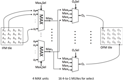
Fig. 5. Hardware architecture of padding/pooling unit.
<details>
<summary>Image 4 Details</summary>
### Visual Description
## Block Diagram: Feature Processing Pipeline
### Overview
The diagram illustrates a multi-stage processing pipeline for feature extraction, likely from a neural network or signal processing system. Input features (IFM tile) are processed through MAX units, selection logic (MUXes), and output feature mapping (OFM tile).
### Components/Axes
- **Input**: IFM tile (8 input channels: A₀ to A₇).
- **Processing Units**:
- **4 MAX units**: Each takes 8 inputs (A₀–A₇) and outputs 4 max values (Max₀–Max₃).
- **16 4-to-1 MUXes**: Select outputs from MAX units based on control signals (Max_sel, O_sel).
- **Output**: OFM tile (8 output channels: O₀ to O₇).
- **Control Signals**:
- Max_sel: Selects between MAX unit outputs.
- O_sel: Selects final output values for OFM tile.
### Detailed Analysis
1. **IFM Tile**:
- 8 input channels (A₀–A₇) are fed into 4 MAX units.
- Each MAX unit processes 2 input channels (e.g., A₀ and A₁ for Max₀).
2. **MAX Units**:
- 4 units, each outputting 4 max values (Max₀–Max₃).
- Outputs are routed to 16 4-to-1 MUXes.
3. **MUXes**:
- 16 MUXes, each with 4 inputs (Max₀–Max₃) and 1 output.
- Controlled by Max_sel and O_sel signals.
4. **OFM Tile**:
- 8 output channels (O₀–O₇) receive selected values from MUXes.
- O_sel determines which MAX outputs are routed to OFM.
### Key Observations
- **Dimensionality Reduction**: 8 input channels → 4 MAX outputs → 16 MUX outputs → 8 OFM outputs.
- **Selection Logic**: MUXes dynamically route MAX outputs based on control signals, enabling adaptive feature selection.
- **Symmetry**: Input and output tiles have identical channel counts (8), suggesting balanced processing.
### Interpretation
This pipeline likely implements a **max-pooling layer** followed by **adaptive feature selection** in a neural network. The MAX units reduce spatial/temporal resolution while preserving dominant features. The 16 MUXes allow fine-grained control over which features propagate to the output, enabling tasks like attention mechanisms or dynamic feature gating. The symmetry between input and output channels suggests the system maintains feature dimensionality after processing, critical for tasks requiring consistent input-output relationships (e.g., classification, regression).
**Notable Design Choices**:
- Use of MAX units for non-linear feature extraction.
- MUXes introduce flexibility in feature routing, potentially enabling context-aware processing.
- Balanced input/output dimensions imply compatibility with subsequent layers in a network architecture.
</details>
given x/y tile position is synchronized using a Pthreads barrier.
## C. Padding and Pooling
Fig. 5 shows the padding/max-pooling unit. The controller/data-staging unit injects an IFM tile (shown on the left), as well as an instruction that specifies the desired padding/max-pooling behavior. There are four MAX units that, based on the instruction, select the maximum of any of the 16 IFM values in the input tile. The MAX units feed 16 multiplexers: one for each value of the OFM tile being computed. Based on the instruction, each value in the OFM tile may be updated with one of the MAX unit outputs, or alternately, may retain its old value.
To implement padding, which does not involve taking the maximum of multiple IFM values, the MAX units return a single value from the IFM (i.e. find the maximum among a single value). The specific number of MAX units (four in this case), is inspired by the needs of VGG-16, which requires 2 × 2 max-pooling regions with a stride of 2. However, with just a few instructions, the padding/max-pooling unit is capable of realizing any padding/max-pooling layer (e.g. a variety of max-pooling region sizes or strides). Moreover, since all units are described in software, it is straightforward to increase the number of MAX functional units within the padding/maxpooling unit.
## IV. IMPLEMENTATION
## A. High-Level Synthesis
Use of the LegUp HLS Pthreads flow permitted accelerator design, development and debugging to proceed in software. Debug and test were simplified, as the parallel software execution aligns closely with the target hardware architecture.
The primary HLS constraints applied were loop pipelining, if-conversion, automated bitwidth minimization [10], and clock-period constraints. To achieve optimized loop pipelines (initiation interval [II] = 1), it was necessary to remove control flow from the C code to the extent possible by making use of the ternary operator ( <cond> ? <val1> : <val2> ) to implement MUX'ing instead of using conditionals. The C specification of the accelerator is ∼ 5,600 LOC. The Verilog RTL automatically produced by LegUp was modified (using a script) in three ways: 1) pragmas were added to direct the Intel synthesis tools to implement the FIFO queues using LUT RAM instead of block RAM (saving precious block-RAM resources); 2) the on-FPGA SRAM banks were brought to the top-level of the hierarchy, making them accessible to the DMA
unit for writing/reading; and 3) the port assignment for the onFPGA RAM banks was altered so that reads and writes have exclusive ports, reducing contention/arbitration. Our design goal was skewed towards maximizing performance; however, it is possible to apply directives in LegUp that lower resource utilization at the expense of some performance.
A challenge with HLS is the disconnect between the software source code and the generated hardware -it can be difficult for one to know how to change the source code to effect desired changes in the hardware. In this work, this issue arose in the context of the controller/data-staging unit, which synthesized to a module with a large number of FSM states (hundreds), and consequent high-fanout signals (e.g. the FSM stall logic). To mitigate this, we split the unit into two C functions, one for convolution instructions and one for padding/max-pooling instructions, each having a simpler FSM than the original monolithic controller.
With reference to Fig. 3, the pool/pad, convolution, writeto-memory, and accumulator units are all streaming kernels generated by LegUp HLS that can accept new inputs every clock cycle (II = 1). The data-staging/control unit is capable of injecting data into the compute units every cycle. We reinforce that the entire accelerator, including the compute pipelines and the relatively complex control as described in Section III-A, is synthesized to Verilog RTL from parallel C software. Manual RTL design was used solely for the DMA unit. While streaming audio/video applications are typically emblematic as being 'ideal' for the use of HLS, here, we show that HLS can effectively be used to generate sophisticated control and data-staging for streaming hardware.
## B. VGG-16 Reduced Precision and Pruning
Beginning with the pre-trained VGG-16 model [3], we increased the sparsity by pruning and reduced the precision to 8-bit magnitude-plus-sign representation by scaling. Pruning and precision reduction were done using Caffe, in a manner similar to [9]. We consider two VGG-16 models: 1) with reduced precision and 2) with reduced precision and pruning. With variant #2, inference accuracy in validation was within 2% of the original unpruned floating point, which can be improved further through training.
## C. Software
Software executing on the on-chip ARM processor handles the loading and pre-processing of network weights, biases and test images. Pre-processing includes the reordering of data into tiled format for our accelerator. The framework sends the instruction and calls the hardware driver for inference.
## D. System Integration, Accelerator Scale-Out
The accelerator core, DMA controller, and host processor communicate via an interconnect network synthesized using Intel's Qsys System Integration tool. Two separate systems are instantiated: System I is a high bandwidth 256-bit bus that performs DMA to and from system DRAM to the accelerator banks. System II is a set of Avalon Memory-Mapped (AMM) interfaces between the host ARM processor and control and status registers on the accelerator core and DMA unit. The accelerator and DMA unit are controlled using System II by the host ARM processor.
We target a mid-range-sized Intel Arria 10 SX660 FPGA, whose size permits us to instantiate two instances of the
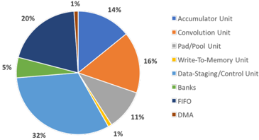
Fig. 6. ALM usage by each unit in the accelerator.
<details>
<summary>Image 5 Details</summary>
### Visual Description
## Pie Chart: Distribution of Components in a Technical System
### Overview
The pie chart illustrates the proportional distribution of various computational units and memory components within a technical system. The chart uses distinct colors to represent each component, with percentages indicating their relative contribution to the system's architecture.
### Components/Axes
- **Legend**: Positioned on the right side of the chart, mapping colors to components:
- **Accumulator Unit**: Dark blue
- **Convolution Unit**: Orange
- **Pad/Pool Unit**: Gray
- **Write-To-Memory Unit**: Yellow
- **Data-Staging/Control Unit**: Light blue
- **Banks**: Green
- **FIFO**: Dark blue
- **DMA**: Brown
- **Axes**: No explicit axes; the chart is circular, with percentages labeled directly on each segment.
### Detailed Analysis
1. **Data-Staging/Control Unit** (32%): Light blue, occupying the largest segment at the bottom of the chart.
2. **Accumulator Unit** (20%): Dark blue, adjacent to the largest segment.
3. **Convolution Unit** (16%): Orange, positioned clockwise from the Accumulator Unit.
4. **Pad/Pool Unit** (14%): Gray, following the Convolution Unit.
5. **Write-To-Memory Unit** (11%): Yellow, smaller segment near the center.
6. **Banks** (5%): Green, a small wedge near the top.
7. **FIFO** (1%): Dark blue, same color as the Accumulator Unit but significantly smaller.
8. **DMA** (1%): Brown, the smallest segment, adjacent to FIFO.
### Key Observations
- The **Data-Staging/Control Unit** dominates the system, comprising over one-third of the components.
- The **Accumulator Unit** and **Convolution Unit** are the next largest contributors, together accounting for 36%.
- The **Write-To-Memory Unit**, **Banks**, **FIFO**, and **DMA** occupy progressively smaller portions, with the latter two at 1% each.
- **Color Conflict**: Both the **Accumulator Unit** (20%) and **FIFO** (1%) are labeled as dark blue in the legend, despite differing significantly in size. This may cause visual ambiguity.
### Interpretation
The chart highlights a hierarchical resource allocation, with the **Data-Staging/Control Unit** as the central component, likely responsible for managing data flow and system coordination. The **Accumulator Unit** and **Convolution Unit** suggest a focus on arithmetic operations and signal processing, respectively. The near-identical color for **Accumulator Unit** and **FIFO** (both dark blue) risks misinterpretation, as their roles and sizes differ drastically. This could indicate a design oversight in the legend or chart labeling. The minimal allocation to **FIFO** and **DMA** (1% each) implies these components are peripheral or optimized for low-overhead functionality. Overall, the system prioritizes data management and computational units over memory and buffering elements.
</details>
accelerator shown in Fig. 3, where each instance operates concurrently on separate stripes of FMs (see Fig. 2). The overall multi-accelerator system is capable of 512 MACs/cycle.
## V. EXPERIMENTAL STUDY
A unique advantage of HLS is that one can synthesize multiple architecture variants from software and constraint changes alone. We analyze area, power and performance for four architecture variants running the two VGG-16 CNN models mentioned above: reduced precision without and with pruning (higher fraction of zero weights). The four architecture variants considered are as follows (labels in brackets):
- 1) A non-optimized simplified accelerator variant with a single convolution sub-module capable of performing at most 16 MACs/cycle (16-unopt).
- 2) A non-performance-optimized variant with one instance of the accelerator in Fig. 3 capable of performing at most 256 MACs/cycle (256-unopt).
- 3) A performance-optimized variant of Fig. 3 (256-opt).
- 4) A variant with two instances of the accelerator in Fig. 3 capable of performing at most 512 MACs/cycle (512-opt).
The 16-unopt architecture computes a single OFM tile at a time, and consequently requires no synchronization among multiple control/data-staging units. Analysis of the 16-unopt architectures gives insight into the HLS hardware quality in the absence of synchronization overhead. Both the 16unopt and the 256-unopt architectures were not performanceoptimized and as such, they consume minimal area and, to verify functional correctness, were clocked at 55MHz. To produce higher-performance variants, we tightened the clockperiod constraint supplied to the LegUp HLS tool, and also invoked performance optimizations in the Intel RTL-synthesis tool: retiming, physical synthesis, higher place/route effort. The 256-opt and 512-opt architectures were clocked at 150 MHz and 120 MHz, respectively. Routing of the 512-opt architecture failed at higher performance targets due to high congestion.
Intel FPGAs have 3 main types of resources: Adaptive Logic Modules (ALMs - lookup-table-based logic), DSP and RAM blocks. Our 256-opt accelerator uses 44% of the ALM logic, 25% of the DSP and 49% of the RAM blocks. Fig. 6 shows the breakdown of ALM usage for each module. The convolution, accumulator and data-staging/control modules take up most of the area, due to the heavy MUX'ing required in these units. Most of the DSP blocks are used in the convolution and accumulator modules. We adjust the RAM block usage to maximize our bank size given the number of available RAMs.
We consider the efficiency of the HLS-generated hardware by comparing the experimentally observed throughput
Fig. 7. Efficiency of each accelerator variant for VGG-16 inference.
<details>
<summary>Image 6 Details</summary>
### Visual Description
## Bar Chart: Effective Efficiency (%) Across Configurations
### Overview
The image is a grouped bar chart comparing the effective efficiency (%) of different configurations across three performance metrics: Best, Mean, and Worst. The chart includes eight categories on the x-axis (e.g., "16-unopt," "16-unopt-pr," etc.) and a y-axis labeled "Effective Efficiency (%)" ranging from 0% to 180%. A dashed horizontal line at 100% is labeled "Ideal," serving as a reference point. The legend at the top right associates colors with the three metrics: Best (dark blue), Mean (light blue), and Worst (red).
### Components/Axes
- **X-axis**: Categories (e.g., "16-unopt," "16-unopt-pr," "256-unopt," "256-unopt-pr," "256-opt," "256-opt-pr," "512-opt," "512-opt-pr").
- **Y-axis**: Effective Efficiency (%) with increments of 20% (0% to 180%).
- **Legend**: Positioned at the top right, with three entries:
- **Best** (dark blue)
- **Mean** (light blue)
- **Worst** (red)
- **Ideal Line**: A dashed horizontal line at 100% labeled "Ideal."
### Detailed Analysis
- **Best (Dark Blue)**:
- All bars exceed 100%, with values ranging from ~95% (16-unopt) to ~160% (16-unopt-pr).
- The highest value is observed in "16-unopt-pr" (~160%), followed by "512-opt-pr" (~140%).
- **Mean (Light Blue)**:
- Bars cluster around 100–120%, with "16-unopt-pr" (~130%) and "512-opt-pr" (~115%) as the highest.
- "16-unopt" (~80%) and "256-unopt" (~90%) are the lowest.
- **Worst (Red)**:
- All bars are below 100%, except "16-unopt-pr" (exactly 100%).
- Values range from ~60% (16-unopt) to ~85% (256-opt-pr).
### Key Observations
1. **Best vs. Ideal**: All "Best" configurations outperform the 100% Ideal line, with "16-unopt-pr" showing the largest deviation (+60%).
2. **Worst vs. Ideal**: Most "Worst" configurations fall significantly below 100%, except "16-unopt-pr" (exactly 100%).
3. **Mean Trends**: The "Mean" metric generally aligns closer to the Ideal line than the "Worst" metric but remains below the "Best" values.
4. **Category Variability**:
- "16-unopt-pr" has the highest "Best" efficiency and the only "Worst" value at 100%.
- "512-opt-pr" shows the highest "Best" efficiency (~140%) and the second-highest "Mean" (~115%).
### Interpretation
The chart demonstrates that configurations labeled "Best" consistently exceed the Ideal efficiency threshold, suggesting optimized performance. The "Worst" configurations underperform, with only "16-unopt-pr" matching the Ideal line. The "Mean" metric reflects a middle ground, indicating variability in performance across the dataset. The outlier in "16-unopt-pr" (Worst = 100%) may indicate a unique case where even the worst-case scenario meets the baseline. This could imply that certain configurations are robust across performance metrics, while others exhibit extreme variability. The data highlights the importance of configuration optimization to achieve or exceed the Ideal efficiency.
</details>
Fig. 8. Absolute GOPS/s across accelerator variants for VGG-16.
<details>
<summary>Image 7 Details</summary>
### Visual Description
## Bar Chart: Effective GOPS
### Overview
The chart compares **Average GOPS** and **Peak GOPS** across different computational configurations. It highlights performance metrics for systems with varying optimization levels and processing capacities (e.g., 16-unopt, 512-opt-pr). The y-axis represents "Effective GOPS" (Giga Operations Per Second), while the x-axis categorizes configurations by optimization and processing scale.
### Components/Axes
- **X-axis**: Configuration types (16-unopt, 16-unopt-pr, 256-unopt, 256-unopt-pr, 256-opt, 256-opt-pr, 512-opt, 512-opt-pr).
- **Y-axis**: "Effective GOPS" (linear scale from 0 to 140).
- **Legend**:
- **Blue (light)**: Average GOPS.
- **Dark Blue**: Peak GOPS.
- **Bar Style**: Grouped bars for each configuration, with Average GOPS on the left and Peak GOPS on the right.
### Detailed Analysis
- **16-unopt**: Average = 1, Peak = 1.
- **16-unopt-pr**: Average = 1, Peak = 2.
- **256-unopt**: Average = 10, Peak = 14.
- **256-unopt-pr**: Average = 14, Peak = 32.
- **256-opt**: Average = 25, Peak = 38.
- **256-opt-pr**: Average = 33, Peak = 86.
- **512-opt**: Average = 40, Peak = 61.
- **512-opt-pr**: Average = 53, Peak = 138.
### Key Observations
1. **Peak GOPS consistently exceed Average GOPS** across all configurations, with the gap widening as configurations scale (e.g., 512-opt-pr: Peak = 138 vs. Average = 53).
2. **Optimization impact**: Configurations with "opt" or "opt-pr" suffixes show significantly higher performance. For example:
- 256-opt-pr: Peak GOPS (86) is 2.6x higher than Average (33).
- 512-opt-pr: Peak GOPS (138) is 2.6x higher than Average (53).
3. **Scaling effect**: Larger configurations (512-opt-pr) achieve the highest metrics, with Peak GOPS reaching 138 (nearly 140 y-axis limit).
4. **Minimal performance**: The least optimized configurations (16-unopt, 16-unopt-pr) have negligible GOPS (1–2).
### Interpretation
The data demonstrates that **optimization and processing scale directly correlate with performance**. Configurations with "opt" or "opt-pr" (likely optimized or pre-optimized systems) achieve substantially higher Peak GOPS, suggesting these settings unlock latent computational capacity. The 512-opt-pr configuration stands out as the most performant, with Peak GOPS nearly tripling the Average. This implies that advanced optimization techniques (e.g., parallel processing, algorithmic improvements) are critical for maximizing throughput. The minimal performance of unoptimized configurations (16-unopt) highlights the importance of system tuning in high-demand scenarios.
</details>
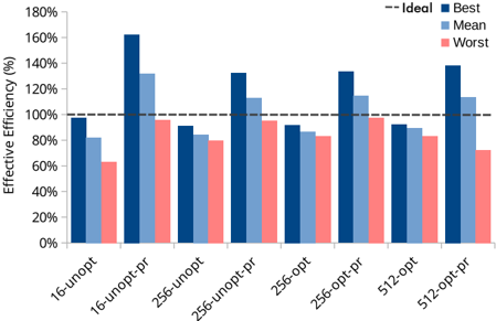
( ops/elapsed time ) with the theoretically minimum ideal throughput numbers. Ideal throughput is defined as peak throughput * total number of computations . We add an overhead ( ∼ 15% but varies by layer) for the increased number of MAC operation due to limited on-FPGA SRAM bank size 'striping'. Results in Fig. 7 illustrate the efficiency of various architectures with the pruned and unpruned VGG-16 model. Results obtained using a pruned network are labeled as '-pr'. 'Best' and 'worst' refer to the highest and lowest throughput for any single convolutional layer of VGG-16, respectively. Mean refers to the average throughput across all VGG-16 layers. The ideal throughput value is indicated as a dotted line on Fig. 7.
The underlying reason for differences between best, worst, and mean is that, for deeper layers of VGG-16, the ratio of weight data to FM data increases, imposing a higher overhead for unpacking weights and offsets in our accelerator, reducing effective throughput. Using the pruned network we see greater than 100% efficiency, due to the zero-skipping avoiding some multiply-accumulates altogether. For the non-pruned VGG-16, we are not far from the ideal throughput -usually within ∼ 10%. This analysis shows the HLS-generated hardware is quite efficient; overhead from HLS is minimal from the cycle latency perspective.
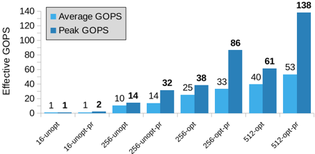
Secondly, we look at our results in terms of absolute performance (GOPS). Fig. 8 shows that our 512-opt accelerator achieved the highest average (peak) throughput of 39.5 GOPS (61 GOPS), and with the pruned network, the effective average (peak) performance increases to 53.3 GOPS (138 GOPS). We can clearly see the effects of zero-skipping in these results. By pruning the network, we were able to increase our performance by ∼ 1.3 × , on average, and ∼ 2.2 × in the
TABLE I. POWER CONSUMPTION
| Accelerator Variant | Peak Power (mW) | GOPS/W | GOPS/W (peak) |
|-----------------------|-------------------|----------|-----------------|
| 256-opt (FPGA) | 2300 (500) | 13.4 | 37.4 |
| 512-opt (FPGA) | 3300 (800) | 13.9 | 41.8 |
| 256-opt (Board) | 9500 | 3.5 | 9.05 |
| 512-opt (Board) | 10800 | 5.6 | 12.7 |
*dynamic power is parenthesized peak case. The peak performance numbers are considerably higher than the average in the pruned case, as peak throughput requires uniformly sparse filters applied concurrently for even workload balancing. Future work could include grouping filters in advance according to similarity in non-zero-entry counts to maximize available zero skipping and balance the work.
While the absolute performance numbers are relatively modest and in line with prior work (cf. Section VI), the results in Fig. 8 underscore a key advantage of HLS, namely, a wide range of architectures with distinct performance/area trade-offs can be produced by software and HLS constraint changes alone. For example, in the opt vs. unopt variants, the clock-period constraint applied in HLS impacts the degree of pipelining in the compute units and control. It would be expensive and time-consuming to produce hand-written RTL for all architecture variants considered. Finally, we note that on a larger Arria 10 FPGA family member (e.g. GT1150), with nearly double the capacity, software changes alone would allow us to scale out the design further.
Power consumption measurements are given in Table I. All measurements are peak power measured while running the accelerator on the worst-case VGG-16 layer. A board -level power measurement is provided, alongside the power consumption of the FPGA by itself. Power numbers in parentheses are dynamic power; numbers outside parentheses are static + dynamic power.
## VI. RELATED WORK
Recent years have seen considerable research on custom hardware accelerators for deep CNN inference designed in manual RTL, realized in ASICs (e.g. [11], [12]) and FPGAs (e.g. [13]). The works most comparable to ours use HLS and target FPGAs. [14] applied Xilinx's Vivado HLS to synthesize an accelerator for the convolution operation, achieving 61 GFLOPS peak performance. Suda et al. [15] synthesized a CNN accelerator from OpenCL, achieving peak performance of 136 GOPS for convolution. In [16], Intel synthesized a CNN accelerator from OpenCL that incorporates the Winograd transform, half-precision floating point, and achieves over 1 TFLOPS performance. In [17], Xilinx synthesized significant parts of a binarized CNN accelerator with Vivado HLS. In binarized CNNs, both weights and activations are represented by 1-bit values. OpenCL along with Xilinx's SDAccel OpenCL HLS tool was also used in [18] to synthesize a single-precision floating-point CNN accelerator incorporating Winograd and achieving 50 GFLOPS performance. The latter work also provides integration with the Caffe framework.
Generally, the OpenCL implementations above use PCIe connectivity with a host processor and are more suited for data center applications; whereas, our system is intended for embedded. To the best of the authors' knowledge, our work is the first to synthesize a CNN accelerator from parallelized C -language software that incorporates a novel zero-skipping approach and reduced precision, and illustrates how, beginning with a software-parallelized C specification of the architecture, constraints to the HLS and RTL synthesis tools can be applied to generate a variety of accelerator architectures with different performance/area trade-offs.
## VII. CONCLUSIONS AND FUTURE WORK
An FPGA-based CNN inference accelerator was synthesized from parallel C software using the LegUp HLS tool, incorporating a zero-weight skipping architecture and reducedprecision arithmetic. The end-to-end system contains a dualcore ARM processor, the accelerator, on-FPGA memories (backed by DDR4) and DMA. Software running on the ARM issues instructions to the accelerator for convolution, padding and pooling. Complex datapath and control logic was synthesized entirely from C , and the use of HLS permitted a range of architectures to be evaluated, through software and constraint changes alone. Future work involves the use of HLS to synthesize accelerators for other neural network styles, including binarized, ternary and recurrent networks.
## REFERENCES
- [1] A. Canis, J. Choi, M. Aldham, V. Zhang, A. Kammoona, T. Czajkowski, S. D. Brown, , and J. H. anderson, 'LegUp: An open source high-level synthesis tool for FPGA-based processor/accelerator systems,' ACM Tranasactions on Embedded Computing Systems , 2013.
- [2] A. Krizhevsky, I. Sutskever, and G. E. Hinton, 'ImageNet classification with deep convolutional neural networks,' in Neural Information Processing Systems , 2012, pp. 1106-1114.
- [3] K. Simonyan and A. Zisserman, 'Very deep convolutional networks for large-scale image recognition,' CoRR , vol. abs/1409.1556, 2014.
- [4] C. Szegedy and et al., 'Going deeper with convolutions,' in IEEE CVPR , 2015, pp. 1-9.
- [5] I. Hubara, M. Courbariaux, D. Soudry, R. El-Yaniv, and Y. Bengio, 'Binarized neural networks,' in NIPS , 2016, pp. 4107-4115.
- [6] G. Venkatesh, E. Nurvitadhi, and D. Marr, 'Accelerating deep convolutional networks using low-precision and sparsity,' CoRR , vol. abs/1610.00324, 2016. [Online]. Available: http://arxiv.org/abs/1610. 00324
- [7] J. Cong, B. Liu, S. Neuendorffer, J. Noguera, K. A. Vissers, and Z. Zhang, 'High-level synthesis for FPGAs: From prototyping to deployment,' IEEE TCAD , vol. 30, no. 4, pp. 473-491, 2011.
- [8] J. Choi, R. Lian, S. D. Brown, and J. H. Anderson, 'A unified software approach to specify pipeline and spatial parallelism in FPGA hardware,' in IEEE ASAP , 2016, pp. 75-82.
- [9] S. Han, H. Mao, and W. J. Dally, 'Deep compression: Compressing deep neural network with pruning, trained quantization and huffman coding,' CoRR , vol. abs/1510.00149, 2015.
- [10] M. Gort and J. H. Anderson, 'Range and bitmask analysis for hardware optimization in high-level synthesis,' in IEEE/ACM ASP-DAC , 2013, pp. 773-779.
- [11] Y. Chen, T. Krishna, J. S. Emer, and V. Sze, 'Eyeriss: An energyefficient reconfigurable accelerator for deep convolutional neural networks,' J. Solid-State Circuits , vol. 52, no. 1, pp. 127-138, 2017.
- [12] T. Chen, Z. Du, N. Sun, J. Wang, C. Wu, Y. Chen, and O. Temam, 'DianNao: A small-footprint high-throughput accelerator for ubiquitous machine-learning,' in ACM ASPLOS , 2014, pp. 269-284.
- [13] E. Nurvitadhi and et al., 'Can FPGAs beat GPUs in accelerating nextgeneration deep neural networks?' in ACM FPGA , 2017, pp. 5-14.
- [14] C. Zhang, P. Li, G. Sun, Y. Guan, B. Xiao, and J. Cong, 'Optimizing FPGA-based accelerator design for deep convolutional neural networks,' in ACM FPGA , 2015, pp. 161-170.
- [15] N. Suda, V. Chandra, G. Dasika, A. Mohanty, Y. Ma, S. Vrudhula, J.-s. Seo, and Y. Cao, 'Throughput-optimized OpenCL-based FPGA accelerator for large-scale convolutional neural networks,' in ACM FPGA , 2016.
- [16] U. Aydonat, S. O'Connell, D. Capalija, A. C. Ling, and G. R. Chiu, 'An OpenCL Deep Learning Accelerator on Arria 10,' ArXiv e-prints , Jan. 2017.
- [17] Y. Umuroglu, N. J. Fraser, G. Gambardella, M. Blott, P. Leong, M. Jahre, and K. Vissers, 'FINN: A Framework for Fast, Scalable Binarized Neural Network Inference,' ArXiv e-prints , 2016.
- [18] R. DiCecco, G. Lacey, J. Vasiljevic, P. Chow, G. W. Taylor, and S. Areibi, 'Caffeinated FPGAs: FPGA framework for convolutional neural networks,' CoRR , vol. abs/1609.09671, 2016.