## p-Bits for Probabilistic Spin Logic
Kerem Y. Camsari, 1 Brian M. Sutton, 1 and Supriyo Datta 1
School of Electrical and Computer Engineering, Purdue University, West Lafayette, IN 47907, USA
(Dated: 13 March 2019)
We introduce the concept of a probabilistic or p-bit, intermediate between the standard bits of digital electronics and the emerging q-bits of quantum computing. We show that low barrier magnets or LBM's provide a natural physical representation for p-bits and can be built either from perpendicular magnets (PMA) designed to be close to the in-plane transition or from circular in-plane magnets (IMA). Magnetic tunnel junctions (MTJ) built using LBM's as free layers can be combined with standard NMOS transistors to provide threeterminal building blocks for large scale probabilistic circuits that can be designed to perform useful functions. Interestingly, this three-terminal unit looks just like the 1T/MTJ device used in embedded MRAM technology, with only one difference: the use of an LBM for the MTJ free layer. We hope that the concept of p-bits and p-circuits will help open up new application spaces for this emerging technology. However, a p-bit need not involve an MTJ, any fluctuating resistor could be combined with a transistor to implement it, while completely digital implementations using conventional CMOS technology are also possible. The p-bit also provides a conceptual bridge between two active but disjoint fields of research, namely stochastic machine learning and quantum computing. First, there are the applications that are based on the similarity of a p-bit to the binary stochastic neuron (BSN), a well-known concept in machine learning. Three-terminal p-bits could provide an efficient hardware accelerator for the BSN. Second, there are the applications that are based on the p-bit being like a poor man's q-bit. Initial demonstrations based on full SPICE simulations show that several optimization problems including quantum annealing are amenable to p-bit implementations which can be scaled up at room temperature using existing technology.
## CONTENTS
| I. | Introduction |
|------|--------------------------------------------|
| | A. Between a bit and a q-bit |
| | B. Binary stochastic neuron (BSN) |
| II. | Hardware Implementation |
| | A. Three-terminal p-Bit |
| | B. Weighted p-bit |
| III. | Applications of p-circuits |
| | A. Applications: Machine learning inspired |
| | B. Applications: Quantum inspired |
| IV. | Conclusions |
| | Acknowledgments |
| V. | References |
## I. INTRODUCTION
## A. Between a bit and a q-bit
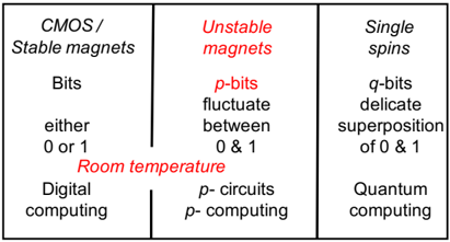
Modern digital circuits are based on binary bits that can take on one of two values, 0 and 1, and are stored using well-developed technologies at room temperature. At the other extreme are quantum circuits based on qbits which are delicate superpositions of 0 and 1 requiring the development of novel technologies typically working at cryogenic temperatures. This article is about what we call probabilistic bits or p-bits that are classical entities fluctuating rapidly between 0 and 1. We will argue that we can use existing technology to build what we call pcircuits that should function robustly at room temperature while addressing some of the applications commonly associated with quantum circuits (Fig. 1).
How would we represent a p-bit physically? Let us first consider the two extremes, namely the bit and the q-bit. A q-bit is often represented by the spin of an electron, while a bit is often represented by binary voltage levels in digital elements like flip-flops and floating-gate transistors. However, bits can also be represented by magnets 1 which are basically collections of a very large number of spins. In a magnet, internal interactions make the energy a minimum when the spins all point either parallel or anti-parallel to a specific direction, called the easy axis. These two directions represent 0 and 1 and are separated by an energy barrier, E b , that ensures their stability.
How large is the barrier? A nanomagnet flips back and forth between 0 and 1 at a rate determined by the energy barrier: τ ∼ τ 0 exp( E b /k B T ) where τ 0 typically has a value between picoseconds and nanoseconds 2 . Assuming a τ 0 of a nanosecond, a barrier of E b ∼ 40 k B T , for example, would retain a 0 (or a 1) for ∼ 10 years, making it suitable for long term memory while a smaller barrier of E b ∼ 14 k B T , would only ensure a short term memory ∼ 1 ms 3 .
It has been recognized that this stability problem also represents an opportunity. Unstable low barrier magnets (LBM) could be used to implement useful functions like random number generation (RNG) 4-6 by sensing the randomly fluctuating magnetization to provide a random time varying voltage. With such applications in mind, we would want magnets to have as low a barrier as possible,
so that many random numbers are generated in a given amount of time. Indeed a 'zero' barrier magnet with E b ≤ k B T flipping back and forth in less than a nanosecond would be ideal.
How can we reduce the energy barrier? Since E b = H K M s Ω / 2, the basic approach is to reduce the total magnetic moment by reducing volume Ω, and/or engineer a small anisotropy field H K 7 . This can be done with perpendicular magnets (PMA) designed to be close to the in-plane transition. A less challenging approach seems to be to use circular in-plane magnets (IMA) 7-9 . We will refer to all these possibilities collectively as LBM's as opposed to say superparamagnets which have more specific connotations in different contexts 3,10-15 .
We could use LBM's to represent the probabilistic bits or p-bits that we alluded to. We have argued that if these p-bits can be incorporated into proper transistor-like structures with gain, then the resulting three-terminal p-bits could be interconnected to build pcircuits that perform useful functions 10,12,16 , not unlike the way transistors are interconnected to build useful digital circuits. However, unlike digital circuits these probabilistic p-circuits incorporate features reminiscent of quantum circuits.
This connection was nicely articulated by Feynman in a seminal paper 17 , where he described a quantum computer that could provide an efficient simulation of quantum many-body problems. But to set the stage for quantum computers, he first described a probabilistic pcomputer which could efficiently simulate classical manybody problems:
. . . 'the other way to simulate a probabilistic nature, which I'll call N . . . is by a computer C which itself is probabilistic, . . . in which the output is not a unique function of the input . . . it simulates nature in this sense: that C goes from some ...initial state . . . to some final state with the same probability that N goes from the corresponding initial state to the corresponding final state . . . If you repeat the same experiment in the computer a large number of times . . . it will give the frequency of a given final state proportional to the number of times, with approximately the same rate . . . as it happens in nature.'
There are many practical problems of great interest which involve large networks of probabilistic quantities. These problems should be simulated efficiently by p-computers of the type envisioned by Feynman. Our purpose here is to discuss appropriate hardware building blocks that can be used to build them 16 and possible applications they could be used for. In this context, let us note that although spins provide a nice unifying paradigm for illustrating the transition from bits to p-bits and q-bits, the physical realization of a p-bit need not involve spins or spintronics; non-spintronic implementations can be just as feasible.
FIG. 1. Between a bit and a q-bit: The p-bit Digital computers use deterministic strings of 0's and 1's called bits to represent information in a binary code. The emerging field of quantum computing is based on q-bits representing a delicate superposition of 0 and 1 that typically requires cryogenic temperatures. We envision a class of probabilistic computers or p-computers operating robustly at room temperature with existing technology based on p-bits which are classical entities fluctuating rapidly between 0 and 1. Although spins provide a nice unifying paradigm for illustrating the transition from bits to p-bits and q-bits, it should be noted that the physical realization of a p-bit need not involve spins or spintronics; non-spintronic implementations can be just as feasible.
<details>
<summary>Image 1 Details</summary>
### Visual Description
## Comparison Diagram: Computing Paradigms
### Overview
The image is a diagram comparing three computing paradigms: CMOS/Stable magnets, Unstable magnets, and Single spins. It contrasts their fundamental units (bits, p-bits, q-bits), behavior, and application areas.
### Components/Axes
The diagram is divided into three vertical sections, each representing a different computing paradigm.
* **Left Section:** CMOS/Stable magnets
* **Middle Section:** Unstable magnets
* **Right Section:** Single spins
Each section contains descriptive text about the paradigm.
### Detailed Analysis
**Left Section: CMOS/Stable magnets**
* **Title:** CMOS/Stable magnets
* **Fundamental Unit:** Bits
* **Behavior:** either 0 or 1
* **Operating Condition:** Room temperature
* **Application:** Digital computing
**Middle Section: Unstable magnets**
* **Title:** Unstable magnets (in red)
* **Fundamental Unit:** p-bits (in red)
* **Behavior:** fluctuate between 0 & 1
* **Operating Condition:** Room temperature (in red)
* **Application:** p- circuits, p- computing
**Right Section: Single spins**
* **Title:** Single spins
* **Fundamental Unit:** q-bits
* **Behavior:** delicate superposition of 0 & 1
* **Application:** Quantum computing
### Key Observations
* The diagram highlights the transition from deterministic bits (0 or 1) in CMOS to probabilistic p-bits (fluctuating between 0 and 1) and quantum q-bits (superposition of 0 and 1).
* The "Unstable magnets" section and the "Room temperature" text are colored red, possibly indicating a challenge or area of focus.
### Interpretation
The diagram illustrates the evolution of computing from classical digital computing (CMOS) to probabilistic computing (p-bits) and quantum computing (q-bits). It emphasizes the fundamental differences in the units of information and their behavior in each paradigm. The use of red color for "Unstable magnets" and "Room temperature" might suggest that these aspects are critical or present challenges in the development of p-bit based computing. The diagram suggests a progression towards more complex and potentially more powerful computing methods.
</details>
| Bits either 0 or 1 CMOS/ Stable magnets | p -bits fluctuate between 0 & 1 Unstable magnets | q -bits delicate of 0 & 1 Single spins |
|-------------------------------------------|----------------------------------------------------|------------------------------------------|
| | | superposition |
| Room temperature | Room temperature | |
| Digital computing | p - circuits p - computing | Quantum computing |
## B. Binary stochastic neuron (BSN)
Interestingly the concept of a p-bit connects naturally to another concept well-known in the field of machine learning, namely that of a binary stochastic neuron (BSN) 18,19 whose response m i to an input I i can be described mathematically by
<!-- formula-not-decoded -->
where r is a random number uniformly distributed between -1 and +1 20 . Here we are using bipolar variables m i = ± 1 to represent the 0 and 1 states. If we use binary variables m i = 0 , 1 the corresponding equation would look different 21 . When combined with a synaptic function described by
<!-- formula-not-decoded -->
we have a probabilistic network that can be designed to perform a wide variety of functions through a proper choice of the weights, W ij . A separate bias term h i is often included in Eq. 2 but we will not write it explicitly, assuming that it is included as the weighted input from an extra p-bit that is always +1.
Eqs. 1 and 2 are widely used in many modern algorithms but they are commonly implemented in software. Much work has gone into developing suitable hardware accelerators for matrix multiplication of the type described by Eq. 2 (See for example, Ref. 22 ). Threeterminal p-bits would provide a hardware accelerator for Eq. 1. Together they would function like a probabilistic computer.
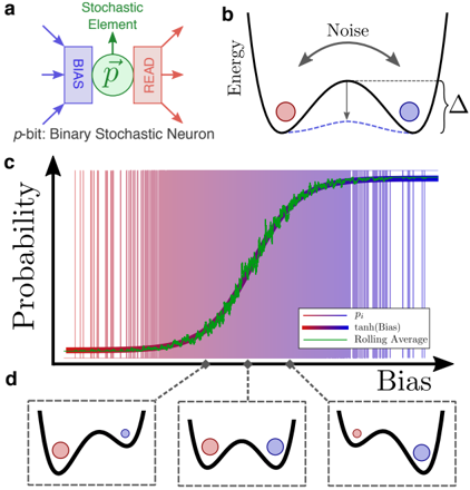
Note that a hardware accelerator for Eq. (1) requires more than just an RNG. We need a tunable RNG whose output m i can be biased through the input terminal I i as shown in Fig. 2. Two distinct designs for a threeterminal p-bit have been described 12,13 both of which use a magnetic tunnel junction (MTJ), a popular 'spintronic' device used in magnetic random access memory (MRAM) 23 . However, MRAM applications use stable MTJ's that can store information for many years, while a p-bit makes use of 'bad' MTJ's with low barriers.
The LBM-based implementation of the BSN described here is conceptually very different from a clocked approach using stable magnets where a stochastic output is obtained every time a clock pulse is applied 16,24-30 . All of these approaches work with stable magnets, although LBM's could be used to reduce the switching power that is needed.
In this paper we will focus on unclocked, asynchronous operation using LBM-based hardware accelerators for the BSN (Eq. (1)) 10-12 . But can an asynchronous circuit provide the sequential updating of the BSN's described by Eq. (1) that is required for Gibbs sampling 31 and is commonly enforced in software through a for loop ? The answer is 'yes' as shown both in SPICE simulations 10 as well as arduino-based emulations 32 , provided the synaptic function in Eq. (2) has a delay that is less than or comparable to the response time of the BSN, Eq. (1).
It should be noted that unclocked operation is a rarity in the digital world and most applications will probably use a clocked, sequential approach with dedicated sequencers that update connected p-bits sequentially. A fully digital implementation of p-circuits using such dedicated sequencers has been realized in Ref. 32 . Synchronous operation can be particularly useful if synaptic delays are large enough to interfere with natural asynchronous operation.
Here, we focus on unclocked operation in order to bring out the role of a p-bit in providing a conceptual bridge between two very active fields of research, namely stochastic machine learning and quantum computing . On the one hand p-bits could provide a hardware accelerator for the BSN (Eq. (1)) thereby enabling applications inspired by machine learning ( Section III ). On the other hand, pbits are the classical analogs of q-bits: robust room temperature entities accessible with current technology that could enable at least some of the applications inspired by quantum computing ( Section IV ). But before we discuss applications, let us briefly discuss possible hardware approaches to implementing p-bits ( Section II ).
## II. HARDWARE IMPLEMENTATION
## A. Three-terminal p-Bit
RNG's represent an important component of modern electronics and have been implemented using many different approaches, including Johnson-Nyquist noise of
FIG. 2. Three terminal p-bit: a. A hardware implementation of the BSN (Eq. (1)) requires a central stochastic element with input and output terminals that provide the ability to read and bias the element. b. The stochastic element can be visualized as going back and forth between two low energy states at a rate that depends exponentially on the barrier E b that separates them: τ = τ 0 exp(∆ /k B T ) c. The bias terminal adjusts the relative energies of the two states thereby controlling the probabilities of finding the element in the two states.
<details>
<summary>Image 2 Details</summary>
### Visual Description
## Stochastic Neuron Diagram
### Overview
The image illustrates the concept of a binary stochastic neuron (p-bit) and its behavior in terms of energy landscapes and probability distributions. It consists of four sub-figures: a schematic of the neuron (a), an energy landscape representation (b), a probability vs. bias plot (c), and three energy landscape examples corresponding to different bias levels (d).
### Components/Axes
**Sub-figure a:**
* **Elements:**
* "BIAS" (blue rectangle): Input to the stochastic element.
* "Stochastic Element" (green circle with "p" inside and an arrow): Represents the core stochastic processing unit.
* "READ" (red rectangle): Output of the neuron.
* **Arrows:** Indicate the flow of information.
* **Label:** "p-bit: Binary Stochastic Neuron" - Describes the overall system.
**Sub-figure b:**
* **Axes:**
* Vertical axis: "Energy"
* **Curve:** A double-well potential energy landscape.
* **Elements:**
* Red and blue circles: Represent the two possible states of the p-bit.
* "Noise" (gray double-headed arrow): Indicates the influence of noise on the system.
* "Δ" (black bracket with label): Represents the energy barrier between the two states.
* Dashed blue line: Represents the energy level of the lower well.
**Sub-figure c:**
* **Axes:**
* Vertical axis: "Probability" (ranging from approximately 0 to 1).
* Horizontal axis: "Bias"
* **Data Series:**
* Red vertical lines: Represent individual samples of the p-bit output.
* Blue line: "tanh(Bias)" - Represents the theoretical probability based on the hyperbolic tangent function of the bias. It is approximately 0 for low bias values and 1 for high bias values.
* Green line: "Rolling Average" - Represents the smoothed probability based on a rolling average of the p-bit output. It follows a sigmoidal curve, transitioning from approximately 0 to 1 as the bias increases.
* **Background:** Gradient from red on the left to blue on the right, visually representing the influence of bias.
* **Legend:** Located in the middle-right of the chart.
**Sub-figure d:**
* Three separate diagrams, each showing a double-well potential energy landscape similar to sub-figure b.
* Each diagram has a red and blue circle representing the two possible states.
* The relative depths of the two wells vary, representing different bias levels.
### Detailed Analysis
**Sub-figure a:**
* The diagram shows a simplified model of a stochastic neuron. The bias input influences the stochastic element, which then produces an output that can be read.
**Sub-figure b:**
* The energy landscape illustrates the two possible states of the p-bit as residing in the two wells. The "Noise" allows the p-bit to transition between these states. The energy barrier "Δ" determines the difficulty of switching states.
**Sub-figure c:**
* **Red Vertical Lines:** These lines are dense on the left side of the chart, indicating a high probability of being in the "red" state (approximately 0 probability). On the right side, the lines are dense, indicating a high probability of being in the "blue" state (approximately 1 probability).
* **Blue Line (tanh(Bias)):** This line starts at approximately 0 for low bias values and gradually increases to approximately 1 for high bias values.
* **Green Line (Rolling Average):** This line closely follows the trend of the blue line but is smoother due to the averaging effect. It starts at approximately 0 and increases to approximately 1 as the bias increases.
* The three gray diamonds on the x-axis of the plot in (c) correspond to the three energy landscapes shown in (d).
**Sub-figure d:**
* The left diagram shows a landscape where the red state has a lower energy than the blue state, corresponding to a low bias.
* The middle diagram shows a landscape where the two states have approximately equal energy, corresponding to an intermediate bias.
* The right diagram shows a landscape where the blue state has a lower energy than the red state, corresponding to a high bias.
### Key Observations
* The probability of the p-bit being in a particular state is directly related to the energy landscape and the applied bias.
* The rolling average provides a smoothed representation of the p-bit's behavior, filtering out some of the noise.
* The tanh(Bias) function provides a theoretical model for the probability, which is closely approximated by the rolling average.
### Interpretation
The image demonstrates how a binary stochastic neuron operates. The bias input shifts the energy landscape, influencing the probability of the neuron being in one of two states. Noise allows the neuron to transition between these states, and the rolling average provides a stable estimate of the probability. The tanh(Bias) function provides a mathematical model for this behavior. The energy landscape diagrams in (d) visually represent how the bias affects the relative stability of the two states. This type of neuron can be used in various applications, such as probabilistic computing and neural networks.
</details>
resistors 33 , phase noise of ring oscillators 34 , process variations of SRAM cells 35 and other physical mechanisms. However, as noted earlier, we need what appears to be a completely new 3-terminal device whose input I i biases its stochastic output m i as shown in Fig. 2c.
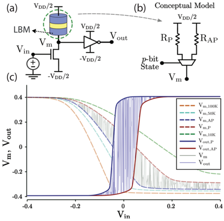
A recent paper 13 shows that such a 3-terminal tunable RNG can be built simply by combining a 2-terminal fluctuating resistance with a transistor (Fig. 3). This seems very attractive at least in the short run, since the basic structure (Fig. 3a) closely resembles the 1T/MTJ structure commonly used for MRAM applications. The first modification that is required is to replace the stable free layer of the MTJ with an LBM. The second modification is to add an inverter to the drain output that amplifies the fluctuations caused by the MTJ resistance.
An MTJ is a device with two magnetic contacts whose electrical resistance R MTJ takes on one of two values R P and R AP depending on whether the magnets are parallel (P) or antiparallel (AP). MTJs are typically used as memory devices, though in recent years applications of MTJs for logic and novel types of computation have been discussed 36-42 .
Standard MTJ devices go to great lengths to ensure that the magnets they use are stable and can store information for many years. The resistance of bad MTJ's, on the other hand, constantly fluctuates between R P and R AP 3 . If we put it in series with a transistor which is
FIG. 3. Embedded MRAM p-bit: a. An NMOS pulldown transistor in series with a stochastic-MTJ whose resistance fluctuates between RP and R AP as shown in b. c. Using a 14 nm HP-FinFET model 43 the input voltage, V in , versus mid-point, V m , and output V out , voltages is simulated in SPICE. Several fixed resistances are shown to convey how V m would vary with modifications to the parallel and antiparallel resistances.
<details>
<summary>Image 3 Details</summary>
### Visual Description
## Circuit Diagram and Transfer Characteristics
### Overview
The image presents a circuit diagram involving a magnetic tunnel junction (MTJ) or LBM (likely Barrier Material), a conceptual model of the circuit, and a plot of the transfer characteristics (Vm, Vout vs. Vin) for different resistance states.
### Components/Axes
* **(a) Circuit Diagram:**
* LBM (Magnetic Tunnel Junction): Represented as a cylinder with two layers of different colors.
* Transistor: An NMOS transistor with the gate connected to Vm, source connected to -VDD/2, and drain connected to the LBM.
* Inverter: An inverter with input VDD/2 and -VDD/2, and output Vout.
* Voltage Source: Vin connected to ground.
* **(b) Conceptual Model:**
* Resistors: Two resistors, Rp and RAP, connected in series.
* p-bit State: A switch controlled by the p-bit state, connecting either Rp or RAP to Vm.
* Voltage Source: VDD/2
* **(c) Transfer Characteristics:**
* X-axis: Vin (Input Voltage), ranging from -0.4 to 0.4.
* Y-axis: Vm, Vout (Output Voltages), ranging from -0.4 to 0.4.
* Legend (Top-Right):
* Vm,100K (dashed orange)
* Vm,50K (dashed cyan)
* Vm,AP (dashed dark blue)
* Vm,P (dashed dark red)
* Vm,10K (dashed green)
* Vout,P (solid dark blue)
* Vout,AP (solid dark red)
* Vm (solid gray)
* Vout (solid light gray)
### Detailed Analysis or Content Details
* **Circuit Diagram (a):**
* The circuit consists of an LBM connected to an NMOS transistor and an inverter. The input voltage Vin controls the transistor, which in turn affects the voltage Vm at the LBM. The inverter outputs Vout based on Vm.
* **Conceptual Model (b):**
* The conceptual model simplifies the LBM as a switch between two resistors, Rp (parallel) and RAP (anti-parallel), representing different resistance states of the MTJ.
* **Transfer Characteristics (c):**
* **Vm,100K (dashed orange):** Starts at approximately 0.4 for Vin = -0.4, gradually decreases to approximately -0.4 as Vin increases to 0.4.
* **Vm,50K (dashed cyan):** Starts at approximately 0.4 for Vin = -0.4, gradually decreases to approximately -0.4 as Vin increases to 0.4.
* **Vm,AP (dashed dark blue):** Starts at approximately 0.4 for Vin = -0.4, gradually decreases to approximately -0.4 as Vin increases to 0.4.
* **Vm,P (dashed dark red):** Starts at approximately 0.4 for Vin = -0.4, gradually decreases to approximately -0.4 as Vin increases to 0.4.
* **Vm,10K (dashed green):** Starts at approximately 0.4 for Vin = -0.4, gradually decreases to approximately -0.4 as Vin increases to 0.4.
* **Vout,P (solid dark blue):** Remains at approximately 0.4 until Vin reaches approximately -0.05, then rapidly decreases to approximately -0.4 as Vin increases to 0.05, and remains at -0.4 for higher Vin values.
* **Vout,AP (solid dark red):** Remains at approximately -0.4 until Vin reaches approximately -0.05, then rapidly increases to approximately 0.4 as Vin increases to 0.05, and remains at 0.4 for higher Vin values.
* **Vm (solid gray):** Similar to Vout,P, but with less sharp transitions.
* **Vout (solid light gray):** Similar to Vout,AP, but with less sharp transitions.
### Key Observations
* The Vm curves for different resistance values (100K, 50K, AP, P, 10K) show a gradual transition from high to low voltage as Vin increases.
* The Vout curves (Vout,P and Vout,AP) exhibit a sharp transition, indicating a switching behavior.
* The Vout,P and Vout,AP curves are inverted with respect to each other, suggesting complementary outputs based on the resistance state of the LBM.
### Interpretation
The image illustrates the operation of a memory cell based on a magnetic tunnel junction (MTJ). The circuit diagram shows how the MTJ is integrated with a transistor and an inverter to create a memory element. The conceptual model simplifies the MTJ as a switch between two resistance states, which are then used to generate different output voltages. The transfer characteristics demonstrate the switching behavior of the circuit, where the output voltage changes sharply based on the input voltage and the resistance state of the MTJ. The different Vm curves for different resistance values likely represent different intermediate states or variations in the MTJ's resistance. The sharp transitions in Vout,P and Vout,AP indicate that the circuit can be used to reliably store and read binary data.
</details>
a voltage controlled resistance R T ( V in ) then the voltage V m (Fig. 3) can be written as
<!-- formula-not-decoded -->
The magnitude of this fluctuating voltage V m is largest when the transistor resistance R T ∼ R P or R AP but gets suppressed if R T R P or if R T R AP . The input voltage controls R T thereby tuning the stochastic output V m as shown in Fig. 3c. It was shown that an additional inverter provides an output that is approximately described by an expression that looks just like the BSN (Eq. 1)
<!-- formula-not-decoded -->
but with dimensionless variables like m i and I i replaced by scaled circuit voltages V out and V in .
The scheme in Fig. 3 provides tunability through the series transistor and does not involve the physics of the fluctuating resistor. Ideally, the magnet is unaffected by the change in the transistor resistance though the drain current, in principle, could pin the magnet. In our simulations that are based on Ref. 13 , we take the pinning current into account through a spin-polarized current ( I s ) proportional to an effective fixed layer polarization and the drain current ( I D ), I s = ( P ) I D ˆ x , where ˆ x is the fixed layer direction. This spin-current enters the sLLG equation that calculates an instantaneous magnetization which in turn controls the MTJ resistance.
We note that any significant pinning around zero input voltage V in,i has to be minimized through proper design, especially for low barrier perpendicular magnets which are relatively easy to pin. Unintentional pinning 44 should in general not be an issue for circular in-plane LBM's due to the strong demagnetizing field. The pinning behavior for the average (steady-state) magnetization can be qualitatively understood by numerical simulations of the sLLG equation. In the case of low-barrier perpendicular magnets the spin-torque pinning needs to overcome the thermal noise and therefore the pinning current is of order I PMA ≈ 2( q/ ) αkT where α is the damping coefficient of the magnet. In the case of circular in-plane magnets, the pinning current is of order I IMA ≈ 2( q/ ) αH D M s Vol . , which is much larger than I PMA since for for typical parameters ( H D M s Vol . kT ).
Since the state of the magnet is not affected, if the input voltage V in,i in Eq. 3 is changed at t=0, the statistics of the output voltage V out,i will respond within tens of picoseconds (typical transistor switching speeds) 45 irrespective of the fluctuation rates of the magnet. However, the magnet fluctuations will determine the correlation time of the random number r in Eq. 3.
Alternatively one can envision structures where the input controls the statistics of the fluctuating resistor itself, through phenomena such as the spin-Hall effect 12 or the magneto-electric effect 46 based on a voltage control of magnetism (see for example 47,48 ). In that case, both the speed of response and the correlation time of the random number r will be determined by the specific phenomenon involved.
Non-spintronic implementations: Note that the structure in Fig. 3 could use any fluctuating resistor including CMOS-based units in place of the MTJ showing that the physical realization of a p-bit need not involve spins 49 . For example, a linear feedback shift register (LFSR) is often used to generate a pseudo-randomly fluctuating bit stream 50 . We can apply this fluctuating voltage to the gate of a transistor to obtain a fluctuating resistor which can replace the MTJ in Fig. 3a. We note that the main appeal of the structure in Fig. 3 lies in its simplicity, since a 1T/1MTJ design coupled with two more transistors provide the tunable randomness in a compact transistorlike building block. Using completely digital p-circuit implementations 32 could offer short term scalability and reliability but they would consume a much larger area and power per p-bit.
## B. Weighted p-bit
The structure in Fig. 3 gives us a 'neuron' that implements Eq. 1 in hardware. Such neurons have to be used in conjunction with a 'synapse' that implements
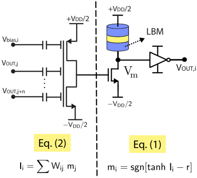
FIG. 4. Example of a weighted p-bit integrating relevant parts of the synapse onto the neurons: Leveraging floating-gate devices along the lines proposed in neuMOS 51 devices, a collection of synapse inputs (from 1 to n) can be summed to produce the bias voltage, V IN ,i for a voltage driven p-bit 52 .
<details>
<summary>Image 4 Details</summary>
### Visual Description
## Circuit Diagram: LBM-Based Neuron Circuit
### Overview
The image presents a circuit diagram of an LBM (likely a Logic-Based Memory or similar) based neuron circuit. The diagram is split into two sections, separated by a dashed vertical line. The left side shows a summation circuit, and the right side shows the LBM and an inverter. The diagram includes voltage labels, component symbols, and mathematical equations.
### Components/Axes
* **Left Side:**
* Input voltages: Vbias,i, VOUT,j, VOUT,j+n (with an ellipsis indicating potentially more inputs).
* Capacitors connected to each input voltage.
* A transistor connected to the capacitors.
* Voltage source: +VDD/2 at the top of the transistor.
* Voltage source: -VDD/2 at the bottom of the transistor.
* **Right Side:**
* LBM (Logic-Based Memory) represented as a cylinder with two distinct layers (likely representing different magnetic states).
* Voltage source: +VDD/2 connected to the top of the LBM.
* Transistor connected to the LBM.
* Voltage source: -VDD/2 at the bottom of the transistor.
* Voltage label: Vm at the connection between the LBM and the transistor.
* Inverter connected to the transistor.
* Output voltage: VOUT,i.
* **Equations:**
* Eq. (2): Ii = Σ Wij mj (located on the left side)
* Eq. (1): mi = sgn[tanh Ii - r] (located on the right side)
### Detailed Analysis or Content Details
* **Left Side (Summation Circuit):**
* Multiple input voltages (Vbias,i, VOUT,j, VOUT,j+n) are connected to capacitors.
* These capacitors are connected to the gate of a transistor.
* The transistor is biased with +VDD/2 at the top and -VDD/2 at the bottom.
* The equation Ii = Σ Wij mj suggests that the transistor is performing a weighted sum of the inputs.
* **Right Side (LBM and Inverter):**
* The LBM is connected to a transistor, which is biased with +VDD/2 and -VDD/2.
* The voltage at the connection between the LBM and the transistor is labeled Vm.
* An inverter is connected to the transistor, producing the output voltage VOUT,i.
* The equation mi = sgn[tanh Ii - r] suggests that the LBM's state (mi) is determined by a hyperbolic tangent function of the input current (Ii) minus a threshold (r), and then passed through a signum function.
* **Voltage Levels:**
* +VDD/2 and -VDD/2 are used as voltage sources in the circuit.
* Vbias,i, VOUT,j, VOUT,j+n, Vm, and VOUT,i are voltage labels at different points in the circuit.
### Key Observations
* The circuit appears to implement a neuron-like function, where the left side performs a weighted sum of inputs, and the right side uses an LBM and an inverter to produce an output.
* The equations provide a mathematical description of the circuit's behavior.
* The LBM is a key component of the circuit, likely providing a non-linear activation function.
### Interpretation
The circuit diagram illustrates a potential implementation of a neuron using an LBM. The left side of the circuit performs a weighted summation of input voltages, which is a common operation in neural networks. The right side of the circuit uses the LBM to introduce a non-linearity, which is also essential for neural network functionality. The equation mi = sgn[tanh Ii - r] suggests that the LBM's state is determined by a hyperbolic tangent function, which is a common activation function in neural networks. The inverter likely serves to invert the signal from the LBM, providing the final output of the neuron. This circuit could be used as a building block for larger neural networks.
</details>
Eq. 2. Alternatively we could design a 'weighted p-bit' that integrates each element of Eq. 1 with the relevant part of Eq. 2. For example, we could use floating gate devices along the lines proposed in neuMOS 51 devices as shown in Fig. 4. From charge conservation we can write
<!-- formula-not-decoded -->
where C 0 is the input capacitance of the transistor. This can be rewritten as
<!-- formula-not-decoded -->
By scaling V in and V out (see Eq. 3) to play the roles of the dimensionless quantities I i and m i respectively, we can recast Eq. 4 in a form similar to Eq. 2:
<!-- formula-not-decoded -->
The weights W ij can be adjusted by controlling the specific capacitors C ij that are connected. The range of allowed weights and connections is then limited by the routing topology and neuMOS device size. Note that the control of weights through C ij works best if C 0 ∑ j C ij so that W i,j ≈ C i,j /C 0 , however it is possible to design a weighted p-bit design without this assumption ( C 0 ∑ C ij ) as discussed in detail in Ref. 52 .
Similar control can also be achieved through a network of resistors. The weights are given by the same expression, but with capacitances C ij replaced by conductances
G ij 22 . However, the input conductance G 0 of FET's is typically very low, so that an external conductance has to be added to make G 0 ∑ j G ij .
## III. APPLICATIONS OF P-CIRCUITS
As noted earlier, real applications involve p-bits interconnected by a synapse that can be implemented off-chip either in software or with a hardware matrix multiplier, but then it is necessary to transfer data back and forth between Eq. 1 and Eq. 2. Therefore, a low-level compact hardware implementation of a p-bit along with a local synapse as envisioned in Fig. 4 could be a hardware accelerator for many types of applications, some of which will be discussed in this section. In the capacitvely weighted p-bit design of Fig. 4, the weights and connectivity of the of the p-bit could be dynamically adjusted based on the encoding of a given problem by leveraging a network of programmable switches 53 as would be encountered in FPGAs. Such a p-bit with local interconnections would look like a compact nanodevice implementation of highly scaled digital spiking neurons of neuromorphic chips such as TrueNorth 54 . Alternatively, the interconnection function could be performed off-chip using standard CMOS devices such as FPGAs or GPUs while p-bits are implemented in a standalone chip by modifying embedded MRAM technology. Note however, the off-chip implementation of the interconnection matrix would impose a timing constraint for an asynchronous mode of operation, which requires the weighted summation operation (Eq. 2) to operate much faster than the p-bit operation (Eq. 1) for proper convergence 10,55 . A full on-chip implementation of a reconfigurable p-bit could function as a low-power, efficient hardware accelerator for applications in Machine Learning and Quantum Computing, but in the near term a heterogenous multi-chip synapse / p-bit combination could also prove to be useful.
Now that we have discussed some possible approaches to implementing Eqs. 1 and 2 in hardware, let us present a few illustrative p-bit networks that can implement useful functions and can be built using existing technology. Unless otherwise stated, these results are obtained from full SPICE simulations 56 that solve the stochastic Landau-Lifshitz-Gilbert equation coupled with the PTMbased transistor models in SPICE 43 to model the embedded MTJ based 3-terminal p-bit described in Fig. 3.
## A. Applications: Machine learning inspired
Bayesian inference: A natural application of stochastic circuits is in the simulation of networks whose nodes are stochastic in nature (See for example 16,57-59 ). An archetypal example is a genetic network, a small version of which is shown in Fig. 5. A well-known concept is that of genetic correlation or relatedness between different members of a family tree. For example, assuming
that each of the children C 1 and C 2 get half their genes from their parents F 1 and M 1 we can write their correlation as:
<!-- formula-not-decoded -->
assuming F 1 and M 1 are uncorrelated. Hence the wellknown result that siblings have 50% relatedness. Similarly one can work out the relatedness of more distant relationships like that of an aunt M 1 and her nephew C 3 which turns out to be 25%.
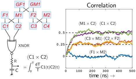
The point is that we could construct a p-circuit with each of the nodes represented by a hardware p-bit interconnected to reflect the genetic influences. The correlation between two nodes, say C 1 and C 2 , is given by
<!-- formula-not-decoded -->
If C 1 (t) and C 2 (t) are binary variables with allowed values of 1 and 0, then they can be multiplied in hardware with an AND gate. If the allowed values are bipolar, -1 and +1, then the multiplication can be implemented with an XNOR gate. In either case the average over time can be performed with a long time constant RCcircuit. A few typical results from SPICE simulations are shown in Fig. 5. The numerical results in Fig. 5 are in good agreement with Bayes theorem even though the circuit operates asynchronously without any sequencers. This is interesting since software simulations of Eqs. 1 and 2 with directed weights usually require the nodes to be updated from parent to child. Whether this behavior generalizes to larger directed networks is left for future work.
We use this genetic circuit as a simple illustration of the concept of nodal correlations which appear in many other contexts in everyday life. Medical diagnosis 60 , for example, involve symptoms such as, say high temperature, which can have multiple origins or parents and one can construct Bayesian networks to determine different causal relationships of interest.
Accelerating learning algorithms: Networks of pbits could be useful in implementing inference networks, where the network weights are trained offline by a learning algorithm in software and the hardware is used to repeatedly perform inference tasks efficiently 61,62 .
Another common example where correlations play an important role is in the learning algorithms used to train modern neural networks like the restricted Boltzmann machine (Fig. 6) 63 having a visible layer and a hidden layer, with connecting weights W ij linking nodes of one layer to those in the other, but not within a layer. A widely used algorithm based on 'contrastive
FIG. 5. Genetic circuit: C1 and C2 are siblings with parents F1, M1, while C3 and C4 are siblings with parents F2, M2. Two of the parents M1 and F2 are siblings with parents GF1, GM1. Genetic correlations between different members can be evaluated from the correlations of the nodal voltages in a p-circuit. An XNOR gate finds their product while a long time constant RC circuit provides the time average.
<details>
<summary>Image 5 Details</summary>
### Visual Description
## Diagram and Chart: Correlation in a System
### Overview
The image presents a combination of a circuit diagram and a correlation chart. The circuit diagram on the left shows a network of interconnected components, culminating in an XNOR gate connected to an RC circuit. The chart on the right displays the correlation between different pairs of signals within the system over time.
### Components/Axes
**Left Side: Circuit Diagram**
* **Nodes:** The diagram features several nodes labeled `GF1`, `GM1`, `F1`, `M1`, `F2`, `M2`, `C1`, `C2`, `C3`, and `C4`. These nodes are interconnected by lines, suggesting signal flow or relationships. The labels are in red.
* **Logic Gate:** An XNOR gate receives inputs from nodes `C1` and `C2`. The output of the XNOR gate is connected to an RC circuit.
* **RC Circuit:** The RC circuit consists of a resistor `R` and a capacitor `C` connected in series to ground.
* **Equation:** Below the XNOR gate, the equation `<C1 x C2> = ∫[0 to T] dT/T C1(t)C2(t)` is displayed.
**Right Side: Correlation Chart**
* **Title:** "Correlation"
* **X-axis:** "time (ns) →" with a scale from 0 to 500 in increments of 100.
* **Y-axis:** The y-axis is not explicitly labeled, but has markers at 0, 0.25, and 0.5.
* **Data Series:** The chart displays four data series, each representing the correlation between different pairs of signals:
* **(M1 x C2) (C1 x C2)**: Green line.
* **(C3 x M1) (C2 x F2)**: Purple line.
* **(F1 x M2)**: Blue line.
* **Horizontal Dashed Lines:** There are two horizontal dashed lines at approximately y = 0.25 and y = 0.5.
### Detailed Analysis
**Circuit Diagram**
* The nodes `GF1` and `GM1` appear to be the starting points of the network.
* `F1` and `M1` are connected to `C1` and `C2`, respectively.
* `F2` and `M2` are connected to `C3` and `C4`, respectively.
* `C1` and `C2` feed into the XNOR gate.
**Correlation Chart**
* **Green Line (M1 x C2) (C1 x C2):** Starts at approximately 0.2, rises sharply to approximately 0.5 within the first 100 ns, and then fluctuates around 0.5.
* **Purple Line (C3 x M1) (C2 x F2):** Starts at approximately 0.1, rises sharply to approximately 0.45 within the first 100 ns, and then fluctuates around 0.45.
* **Orange Line (C3 x M1) (C2 x F2):** Starts at approximately 0.1, rises sharply to approximately 0.25 within the first 100 ns, and then fluctuates around 0.25.
* **Blue Line (F1 x M2):** Starts at approximately 0, fluctuates around 0 throughout the entire time range.
### Key Observations
* The green and purple lines show a strong positive correlation that develops quickly.
* The orange line shows a moderate positive correlation.
* The blue line shows almost no correlation.
* The correlations seem to stabilize after approximately 100 ns.
### Interpretation
The image suggests an analysis of signal correlations within a system represented by the circuit diagram. The chart indicates that certain signal pairs (M1 x C2, C1 x C2, C3 x M1, C2 x F2) exhibit significant positive correlation, implying a strong relationship or dependency between them. The signal pair F1 x M2, however, shows negligible correlation, suggesting independence or a weak relationship. The equation provided likely represents the method used to calculate the correlation between signals C1 and C2 over a time period T. The RC circuit connected to the XNOR gate likely serves as a filter or integrator, influencing the signals being analyzed. The rapid rise in correlation for the green and purple lines suggests a fast response or strong coupling between the corresponding signals.
</details>
divergence' 64 adjusts each weight W ij according to
<!-- formula-not-decoded -->
which requires the repeated evaluation of the correlations 〈 v i h j 〉 . Computing such correlations exactly becomes intractable due to their exponential complexity in the number of neurons, therefore contrastive divergence is often limited by a fixed number of steps (CDn) to limit the number of repeated evaluation of these correlations. This process could be accelerated through an efficient physical representation of the neuron and the synapse 65,66 .
## B. Applications: Quantum inspired
The functionality of neural networks is determined by the weight matrix W ij which determines the connectivity among the neurons. They can be classified broadly by the relation between W ij and W ji . In traditional feedforward networks, information flow is directed with neuron 'i' influencing neuron 'j' through a non-zero weight W ij but with no feedback from neuron 'j' , such that W ji = 0. At the other end of the spectrum, is a network with all connections being reciprocal W ij = W ji . In between these two extremes are the class of networks for which the weights between two nodes are asymmetric, but non-zero.
The class of networks with symmetric connections is particularly interesting since they have a close parallel with classical statistical physics where the natural connections between interacting particles is symmetric and the equilibrium probabilities are given by the celebrated Boltzmann law expressing the probability of a particular configuration α in terms of an energy E α associated with
FIG. 6. Restricted Boltzmann Machine (RBM): RBMs are a special class of stochastic neural networks that restrict connections within a hidden and a visible layer. Standard learning algorithms require repeated evaluations of correlations of the form 〈 v i h j 〉 .
<details>
<summary>Image 6 Details</summary>
### Visual Description
## Diagram: Restricted Boltzmann Machine (RBM) Architecture
### Overview
The image depicts a simplified architecture of a Restricted Boltzmann Machine (RBM). It shows two layers: a visible layer (v) and a hidden layer (h), with connections between them. The diagram illustrates the probabilistic connections between the visible units and the hidden units.
### Components/Axes
* **Top Layer (Visible Layer):** A blue rectangle labeled with "v1" on the left, "vn" on the right, and "..." in the middle.
* **Bottom Layer (Hidden Layer):** A green rectangle labeled with "h1" on the left, "hm" on the right, and "..." in the middle.
* **Connections:** Arrows pointing from the hidden layer to the visible layer and from the visible layer to the hidden layer.
### Detailed Analysis or ### Content Details
* **Visible Layer:** The visible layer consists of 'n' units, denoted as v1 to vn.
* **Hidden Layer:** The hidden layer consists of 'm' units, denoted as h1 to hm.
* **Connections:** The arrows indicate bidirectional connections between the visible and hidden layers. Specifically, there are arrows from h1 to v1 and vn, and arrows from v1 and vn to hm.
### Key Observations
* The diagram shows a bipartite graph structure, where connections exist only between the visible and hidden layers, and not within each layer.
* The "..." notation indicates that there are multiple units in each layer, but only the first and last units are explicitly labeled.
### Interpretation
The diagram illustrates the basic architecture of an RBM, which is a generative stochastic neural network. The visible layer represents the input data, while the hidden layer learns to extract features from the input. The bidirectional connections allow the RBM to learn a probability distribution over the input data. The absence of connections within each layer is a key characteristic of RBMs, simplifying the learning process. The diagram highlights the relationship between the visible and hidden units and the flow of information between them.
</details>
that configuration.
<!-- formula-not-decoded -->
<!-- formula-not-decoded -->
where T denotes transpose and the constant Z is chosen to ensure that all P ′ α s add up to one. This energy principle is only available for reciprocal networks 67 , and can be very useful in determining the appropriate weights W ij for a particular problem.
This class of networks connects naturally to the world of quantum computing which is governed by Hermitian Hamiltonians, and is also the subject of the emerging field of Ising computing 10,16,68-72 .
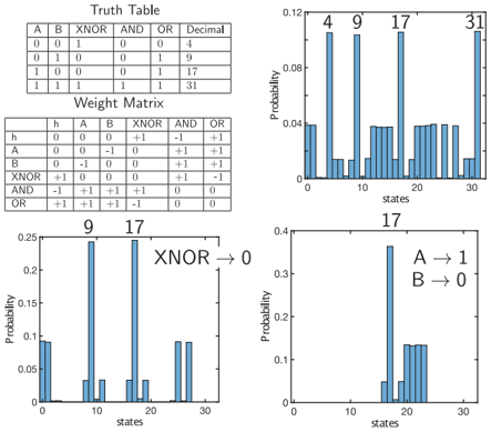
Invertible Boolean logic: Suppose, for example, we wish to design a Boolean gate which will provide three outputs reflecting the AND, OR and XNOR functions of the two inputs A and B. The truth table is shown in Fig. 7. Note that although we are using the binary notation 1 and 0, they actually stand for p-bit values of +1 and -1 respectively.
Since there are five p-bits, two representing the inputs and three representing the outputs, the system has 2 5 = 32 possible states, which can be indexed by their corresponding decimal values. Each of these configurations has an associated energy, E n , n = 0 , 1 , . . . , 31 . What we need is a weight matrix W ij such that the desired configurations 4, 9, 17 and 31 (in decimal notation) specified by the truth table have a low energy E α (Eq. (8)) compared to the rest, so that they are occupied with higher probability. This can be done either by using the principles of linear algebra 12 or by using machine learning algorithms 73 to obtain the weight matrix shown in Fig. 7. Note that an additional p-bit labeled 'h' has been introduced which is clamped to a value of +1 by applying a large bias.
On the right of Fig. 7, a histogram is showing the frequency of all the possible (32) configurations obtained from a simulation of Eq. (1) and Eq. (2) using this weight matrix. Similar results are obtained from a SPICE simulation of a p-circuit of weighted p-bits. Note the peaks at the desired truth table values, with smaller peaks at some of the undesired values. The peaks closely follow
FIG. 7. Invertible Boolean logic: A multi-function Boolean gate with 6 p-bits is shown. Inputs A and B produce the output for a 2-input XNOR, AND and OR gate, respectively. The handle bit, 'h' is used to remove the complementary low-energy states that do not belong to the truth table shown. In the unclamped mode, the system shows the states corresponding to the the lines of the truth table with high probability. A and B can be clamped to produce the correct output for the XNOR, AND and OR in the direct mode. In the inverse mode, any one of the outputs (XNOR is shown as an example) can be clamped to a given value, and the inputs fluctuate among possible input combinations corresponding to this output.
<details>
<summary>Image 7 Details</summary>
### Visual Description
## Truth Table, Weight Matrix, and Probability Distribution Charts
### Overview
The image presents a truth table, a weight matrix, and three probability distribution charts. The truth table defines the logical operations XNOR, AND, and OR for two binary inputs A and B. The weight matrix shows the relationships between the inputs, outputs, and a hidden variable 'h'. The probability distribution charts display the probability of different states, with annotations indicating specific conditions or outputs.
### Components/Axes
**1. Truth Table:**
* **Columns:** A, B, XNOR, AND, OR, Decimal
* **Rows:** Four rows representing all possible combinations of A and B (00, 01, 10, 11).
* **Decimal Values:** 4, 9, 17, 31 corresponding to the binary combinations.
**2. Weight Matrix:**
* **Rows/Columns:** h, A, B, XNOR, AND, OR
* **Values:** +1, -1, and 0 representing the strength and direction of the relationship between the variables.
**3. Probability Distribution Charts:**
* **X-axis:** States (ranging from 0 to 30, with tick marks every 10 units)
* **Y-axis:** Probability (ranging from 0 to 0.12 in the top chart, 0 to 0.25 in the bottom-left chart, and 0 to 0.4 in the bottom-right chart)
* **Bars:** Blue bars representing the probability of each state.
* **Annotations:** Numerical values (4, 9, 17, 31) above specific bars in the top chart, and text annotations in the bottom charts ("XNOR -> 0", "A -> 1", "B -> 0").
### Detailed Analysis
**1. Truth Table:**
| A | B | XNOR | AND | OR | Decimal |
| --- | --- | ---- | --- | --- | ------- |
| 0 | 0 | 1 | 0 | 0 | 4 |
| 0 | 1 | 0 | 0 | 1 | 9 |
| 1 | 0 | 0 | 0 | 1 | 17 |
| 1 | 1 | 1 | 1 | 1 | 31 |
**2. Weight Matrix:**
| | h | A | B | XNOR | AND | OR |
| :---- | :- | :- | :- | :--- | :-: | :-: |
| h | 0 | 0 | 0 | +1 | -1 | +1 |
| A | 0 | 0 | -1 | 0 | +1 | +1 |
| B | 0 | -1 | 0 | 0 | +1 | +1 |
| XNOR | +1 | 0 | 0 | 0 | +1 | -1 |
| AND | -1 | +1 | +1 | +1 | 0 | 0 |
| OR | +1 | +1 | +1 | -1 | 0 | 0 |
**3. Probability Distribution Charts:**
* **Top Chart:**
* The probability is high at states 4, 9, 17, and 31, with approximate probabilities of 0.11.
* The probability is low for most other states, with probabilities around 0.04.
* **Bottom-Left Chart:**
* The probability is high at states 0, 9, and 17, with approximate probabilities of 0.09, 0.23, and 0.23 respectively.
* The probability is low for most other states, with probabilities around 0.03.
* Annotation: "XNOR -> 0"
* **Bottom-Right Chart:**
* The probability is high at state 17, with an approximate probability of 0.37.
* The probability is low for most other states, with probabilities around 0.12.
* Annotation: "A -> 1", "B -> 0"
### Key Observations
* The truth table defines the logical operations and their corresponding decimal values.
* The weight matrix shows the relationships between the variables, with positive values indicating positive correlations and negative values indicating negative correlations.
* The probability distribution charts show the probability of different states under specific conditions.
* The annotations on the charts provide additional information about the conditions or outputs being represented.
### Interpretation
The data suggests that the probability distribution charts are showing the probability of different states based on the truth table and weight matrix. The top chart shows the probability of states corresponding to the decimal values of the truth table rows. The bottom charts show the probability of states under specific conditions, such as when XNOR is 0, A is 1, and B is 0. The relationships between the variables in the weight matrix may be influencing the probability distributions. The high probabilities at specific states indicate that those states are more likely to occur under the given conditions.
</details>
the Boltzmann law, such that
<!-- formula-not-decoded -->
Undesired peaks can be suppressed if we make the Wmatrix larger, say by an overall multiplicative factor of 2. If all energies are increased by a factor of 2, the ratio of probabilities would be squared: a ratio of 10 would become a ratio of 100.
It is also possible to operate the gate in a traditional feed-forward manner where inputs are specified and an output is obtained. This mode is shown in the middle panel on the right where the inputs A and B are clamped to 1 and 0 respectively. Only one of the four truth table peaks can be seen, namely the line corresponding to A=1, B=0, which is labeled 17.
What is more interesting is that the gates can be run in inverse mode as shown in the lower right panel. The XNOR output is clamped to 0 corresponding to specific lines of the truth table corresponding to 9 and 17. The inputs now fluctuate between the two possibilities, indicating that we can use these gates to provide us with all possible inputs consistent with a specified output, a mode of operation not possible with standard Boolean gates.
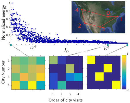
FIG. 8. Combinatorial Optimization: A 5-city Traveling Salesman Problem (TSP) implemented using a network of 16 p-bits (fixing city 0), each having two indices, the first denoting the order in which a city is visited and the second denoting the city. The interaction parameter I 0 scales all weights and acts as an inverse temperature and is slowly increased via a simple annealing schedule I 0 ( t + t eq ) = ( 1 / 0 . 99 ) I 0 ( t ) to guide the system into the lowest energy state, providing the shortest traveling distance (Map imagery data: Google, TerraMetrics).
<details>
<summary>Image 8 Details</summary>
### Visual Description
## Scatter Plot with Heatmaps and Map: Energy vs. I0 with City Visit Order
### Overview
The image presents a scatter plot showing the relationship between normalized energy and a parameter I0, accompanied by three heatmaps visualizing city visit order and a map illustrating city locations and routes. The scatter plot shows a negative correlation between normalized energy and I0. The heatmaps display different patterns of city visit order, and the map shows a route connecting five cities.
### Components/Axes
**1. Scatter Plot:**
* **X-axis:** I0 (logarithmic scale). Axis markers are approximately 10^-1, 10^0, and 10^1.
* **Y-axis:** Normalized energy. Axis markers are 0, 0.2, 0.4, 0.6, 0.8, and 1.
* **Data:** Blue dots representing data points.
**2. Heatmaps (Bottom Row):**
* **X-axis:** Order of city visits (1, 2, 3, 4).
* **Y-axis:** City Number (1, 2, 3, 4).
* **Color Scale:** Ranges from -1 (dark blue) to 1 (yellow).
* **Heatmap 1 (Left):** Shows a gradient of colors, indicating varying degrees of correlation or interaction between city number and visit order.
* **Heatmap 2 (Middle):** Shows a more discrete pattern with predominantly blue and some green/yellow squares.
* **Heatmap 3 (Right):** Shows a distinct pattern with yellow squares along the diagonal and blue squares elsewhere.
**3. Map (Top-Right):**
* Shows a geographical map of the United States.
* Five cities are marked with numbers 0, 1, 2, 3, and 4.
* Red lines connect the cities, indicating a route.
### Detailed Analysis
**1. Scatter Plot:**
* The blue data points form a dense cloud that decreases rapidly as I0 increases from approximately 0.01 to 0.1.
* As I0 increases from 0.1 to 1, the density of data points decreases, and the normalized energy approaches 0.
* The trend is a negative correlation between normalized energy and I0.
**2. Heatmaps:**
* **Heatmap 1:**
* City 1: Shows a gradient from green to yellow as the order of visits increases.
* City 2: Shows a gradient from green to yellow as the order of visits increases.
* City 3: Shows a gradient from orange to yellow as the order of visits increases.
* City 4: Shows a gradient from green to yellow as the order of visits increases.
* **Heatmap 2:**
* City 1: Visit order 1 is green, the rest are blue.
* City 2: Visit order 3 is green, the rest are blue.
* City 3: Visit order 2 is green, the rest are blue.
* City 4: Visit order 4 is green, the rest are blue.
* **Heatmap 3:**
* City 1: Visit order 1 is yellow, the rest are blue.
* City 2: Visit order 2 is yellow, the rest are blue.
* City 3: Visit order 3 is yellow, the rest are blue.
* City 4: Visit order 4 is yellow, the rest are blue.
**3. Map:**
* City 0 is located in the northeastern United States.
* City 1 is located on the east coast.
* City 2 is located in California.
* City 3 is located in the southwestern United States.
* City 4 is located in the northwestern United States.
* The route connects the cities in the order 0 -> 1 -> 3 -> 2 -> 4 -> 0.
### Key Observations
* The scatter plot shows a clear negative correlation between normalized energy and I0.
* The heatmaps display different patterns of city visit order, suggesting different optimization strategies or constraints.
* The map provides a geographical context for the city visit order.
### Interpretation
The data suggests that as the parameter I0 increases, the normalized energy decreases. This could indicate that a higher value of I0 leads to a more efficient or stable state. The heatmaps provide insights into the relationship between city number and visit order, potentially reflecting different optimization strategies for the traveling salesman problem or a similar routing problem. The map provides a visual representation of the cities and the route connecting them, allowing for a better understanding of the geographical context of the problem. The different patterns in the heatmaps could represent different stages of an optimization process or different solutions to the problem. Heatmap 3, with the yellow diagonal, suggests a scenario where each city is visited in its corresponding order (City 1 is visited first, City 2 is visited second, etc.).
</details>
This invertible mode is particularly interesting because there are many cases where the direct problem is relatively easy compared to the inverse problem. For example, we can find a suitable weight matrix to implement an adder that provides the sum S of numbers A, B and C. But the same network also solves the inverse problem where a sum S is provided and it finds combinations of k numbers that add up to S 32,52 . This inverse k-sum or subset sum problem is known to be NP-complete 74 and is clearly much more difficult than direct addition. Similarly we can design a weight matrix such that the network multiplies any two numbers. In inverse mode the same network can factorize a given number, which is a hard problem 75 . This ability to factorize has been shown with relatively small numbers 12,32 . How well p-circuits will scale to larger factorization problems remains to be explored.
It is worth mentioning that this method of solving integer factorization and the subset sum problem is similar to the deterministic 'memcomputing' framework where a 'self-organizing logic circuit' is set up to solve the direct problem and operated in reverse to solve the inverse problem (See for example, Ref. 76,77 ).
Optimization by classical annealing: It has been shown that many optimization problems can be mapped onto a network of classical spins with an appropriate weight matrix, such that the optimal solution corresponds to the configuration with the lowest energy 78 . Indeed, even the problem of integer factorization discussed above in terms of inverse multiplication can alternatively be addressed in this framework by casting it as an optimization problem 79-81 .
A well-known example of an optimization problem is the classic N-city traveling salesman problem (TSP). It involves finding the shortest route by which a salesman can visit all cities once starting from a particular one. This problem has been mapped to a network of ( N -1) 2 spins where each spin has two indices, the first denoting the order in which a city is visited and the second denoting the city.
Fig. 8 shows a 5-city TSP mapped to a 16 p-bit network and translated into a p-circuit that is simulated using SPICE. The overall W-matrix is slowly increased and with increasing interaction the network gradually settles from a random state into a low energy state. This process is often called simulated annealing 82 based on the similarity with the freezing of a liquid into a solid with a lowering of temperature in the physical world, which reduces the random thermal energy relative to a fixed interaction.
Note that at high values of interaction the p-bits settle to the correct solution with four p-bits highlighted corresponding to (1,1), (2,3), (3,2) and (4,4), showing that the cities should be visited in the order 1-3-2-4. Unfortunately things may not work quite so smoothly as we scale up to problems with larger numbers of p-bits. The system tends to get stuck in metastable states just as in the physical world solids develop defects that keep them from reaching the lowest energy state.
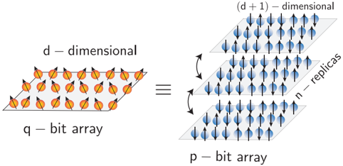
Optimization by quantum annealing: An approach that has been explored is the process of quantum annealing using a network of quantum spins implemented with superconducting q-bits 83,84 . However, it is known that for certain classes of quantum problems classified by 'stoquastic' Hamiltonians 85 , a network of q-bits can be approximated with a larger network of p-bits operating in hardware (Fig. 9) 86 . We have made use of this equivalence to design p-circuits whose SPICE simulations show correlations and averages comparable to those obtained with quantum annealers 86 .
## IV. CONCLUSIONS
In summary, we have introduced the concept of a probabilistic or p-bit, intermediate between the standard bits of digital electronics and the emerging q-bits of quantum computing. Low barrier magnets or LBM's provide a natural physical representation for p-bits and can be built either from perpendicular magnets (PMA) designed to be close to the in-plane transition or from circular in-plane magnets (IMA). Magnetic tunnel junctions (MTJ) built using LBM's as free layers can be combined with standard NMOS transistors to provide three-terminal building blocks for large scale probabilistic circuits that can be designed to perform useful functions. Interestingly, this three-terminal unit looks just like the 1T/MTJ de-
FIG. 9. Mapping a q-bit network into a p-bit network : A special class of quantum many body Hamiltonians that are 'stoquastic' can be solved by mapping them to a classical network of p-bits that consist of a finite number of replicas of the original system that are interacting in the 'vertical' direction. This approach implemented in software is also known as the Path Integral Monte Carlo method. A hardware implementation would constitute a p-computer that is capable of performing quantum annealing 86 .
<details>
<summary>Image 9 Details</summary>
### Visual Description
## Diagram: Dimensionality and Bit Array Representation
### Overview
The image illustrates the relationship between a 'd-dimensional' and a '(d+1)-dimensional' bit array representation. The left side shows a single layer representing a 'q-bit array', while the right side shows a stack of 'n-replicas' representing a 'p-bit array'. The equivalence between the two representations is visually emphasized.
### Components/Axes
* **Left Side:**
* **Array Type:** d-dimensional, q-bit array
* **Elements:** Orange spheres with black arrows pointing in various directions. The spheres are arranged in a grid pattern on a light gray plane.
* **Center:**
* **Symbol:** An equals sign (=) indicating equivalence.
* **Right Side:**
* **Array Type:** (d+1)-dimensional, p-bit array, n-replicas
* **Elements:** Blue spheres with black arrows pointing downwards. The spheres are arranged in a grid pattern on three stacked light gray planes.
* **Replicas:** Three layers are stacked vertically, labeled as 'n - replicas' on the right side.
* **Arrows:** Curved black arrows on the left side of the stacked arrays indicate the relationship between the layers.
### Detailed Analysis
* **Left Array (d-dimensional, q-bit array):**
* The array consists of 5 rows and 5 columns of orange spheres, totaling 25 spheres.
* Each sphere has a black arrow indicating a direction, which varies from sphere to sphere.
* **Right Array ((d+1)-dimensional, p-bit array):**
* The array consists of three layers (n-replicas).
* Each layer has 5 rows and 5 columns of blue spheres, totaling 25 spheres per layer.
* Each sphere has a black arrow pointing downwards.
* The layers are stacked vertically, suggesting an additional dimension.
### Key Observations
* The left side represents a lower-dimensional array with variable arrow directions, while the right side represents a higher-dimensional array with uniform arrow directions.
* The number of spheres in each layer of the right array is the same as the number of spheres in the left array (25).
* The 'n-replicas' label suggests that the number of layers can vary.
### Interpretation
The diagram illustrates a concept of representing a lower-dimensional bit array (q-bit array) as a higher-dimensional array (p-bit array) using multiple replicas. The equivalence sign suggests that both representations are functionally equivalent, but the higher-dimensional representation might offer advantages in certain contexts, such as error correction or parallel processing. The arrows represent the state of each bit, and the change in arrow direction from variable to uniform suggests a transformation or encoding process. The 'n-replicas' indicate that the higher-dimensional representation can be scaled by increasing the number of layers.
</details>
vice used in embedded MRAM technology, with only one difference: the use of an LBM for the MTJ free layer. We hope that this concept will help open up new application spaces for this emerging technology. However, a p-bit need not involve an MTJ, any fluctuating resistor could be combined with a transistor to implement it. It may be interesting to look for resistors that can fluctuate faster based on entities like natural and synthetic antiferromagnets 87,88 , for example.
The p-bit also provides a conceptual bridge between two active but disjoint fields of research, namely stochastic machine learning and quantum computing. This viewpoint suggests two broad classes of applications for p-bit networks. First, there are the applications that are based on the similarity of a p-bit to the binary stochastic neuron (BSN), a well-known concept in machine learning. Three-terminal p-bits could provide an efficient hardware accelerator for the BSN. Second, there are the applications that are based on the p-bit being like a poor man's q-bit. We are encouraged by the initial demonstrations based on full SPICE simulations that several optimization problems including quantum annealing are amenable to p-bit implementations which can be scaled up at room temperature using existing technology.
## ACKNOWLEDGMENTS
S.D. is grateful to Dr. Behtash Behin-Aein for many stimulating discussions leading up to Ref 16 .
## V. REFERENCES
- 1 E. Chen, D. Apalkov, Z. Diao, A. Driskill-Smith, D. Druist, D. Lottis, V. Nikitin, X. Tang, S. Watts, S. Wang, S. Wolf,
A. W. Ghosh, J. Lu, S. J. Poon, M. Stan, W. Butler, S. Gupta, C. K. A. Mewes, T. Mewes, and P. Visscher, 'Advances and Future Prospects of Spin-Transfer Torque Random Access Memory,' IEEE Transactions on Magnetics 46 , 1873-1878 (2010).
- 2 L. Lopez-Diaz, L. Torres, and E. Moro, 'Transition from ferromagnetism to superparamagnetism on the nanosecond time scale,' Physical Review B 65 , 224406 (2002).
- 3 N. Locatelli, A. Mizrahi, A. Accioly, R. Matsumoto, A. Fukushima, H. Kubota, S. Yuasa, V. Cros, L. G. Pereira, D. Querlioz, et al. , 'Noise-enhanced synchronization of stochastic magnetic oscillators,' Physical Review Applied 2 , 034009 (2014).
- 4 B. Parks, M. Bapna, J. Igbokwe, H. Almasi, W. Wang, and S. A. Majetich, 'Superparamagnetic perpendicular magnetic tunnel junctions for true random number generators,' AIP Advances 8 , 055903 (2018), https://doi.org/10.1063/1.5006422.
- 5 D. Vodenicarevic, N. Locatelli, A. Mizrahi, J. Friedman, A. Vincent, M. Romera, A. Fukushima, K. Yakushiji, H. Kubota, S. Yuasa, S. Tiwari, J. Grollier, and D. Querlioz, 'LowEnergy Truly Random Number Generation with Superparamagnetic Tunnel Junctions for Unconventional Computing,' Physical Review Applied 8 , 054045 (2017).
- 6 D. Vodenicarevic, N. Locatelli, A. Mizrahi, T. Hirtzlin, J. S. Friedman, J. Grollier, and D. Querlioz, 'Circuit-Level Evaluation of the Generation of Truly Random Bits with Superparamagnetic Tunnel Junctions,' in 2018 IEEE International Symposium on Circuits and Systems (ISCAS) (2018) pp. 1-4.
- 7 P. Debashis, R. Faria, K. Y. Camsari, and Z. Chen, 'Designing stochastic nanomagnets for probabilistic spin logic,' IEEE Magnetics Letters (2018).
- 8 R. P. Cowburn, D. K. Koltsov, A. O. Adeyeye, M. E. Welland, and D. M. Tricker, 'Single-domain circular nanomagnets,' Physical Review Letters 83 , 1042 (1999).
- 9 P. Debashis, R. Faria, K. Y. Camsari, J. Appenzeller, S. Datta, and Z. Chen, 'Experimental demonstration of nanomagnet networks as hardware for Ising computing,' in 2016 IEEE International Electron Devices Meeting (IEDM) (2016) pp. 34.3.134.3.4.
- 10 B. Sutton, K. Y. Camsari, B. Behin-Aein, and S. Datta, 'Intrinsic optimization using stochastic nanomagnets,' Scientific Reports 7 , 44370 (2017).
- 11 R. Faria, K. Y. Camsari, and S. Datta, 'Low-barrier nanomagnets as p-bits for spin logic,' IEEE Magnetics Letters 8 , 1-5 (2017).
- 12 K. Y. Camsari, R. Faria, B. M. Sutton, and S. Datta, 'Stochastic p -Bits for Invertible Logic,' Physical Review X 7 (2017), 10.1103/PhysRevX.7.031014.
- 13 K. Y. Camsari, S. Salahuddin, and S. Datta, 'Implementing pbits With Embedded MTJ,' IEEE Electron Device Letters 38 , 1767-1770 (2017).
- 14 A. Mizrahi, T. Hirtzlin, A. Fukushima, H. Kubota, S. Yuasa, J. Grollier, and D. Querlioz, 'Neural-like computing with populations of superparamagnetic basis functions,' Nature communications 9 , 1533 (2018).
- 15 M. Bapna and S. A. Majetich, 'Current control of time-averaged magnetization in superparamagnetic tunnel junctions,' Applied Physics Letters 111 , 243107 (2017).
- 16 B. Behin-Aein, V. Diep, and S. Datta, 'A building block for hardware belief networks,' Scientific Reports 6 , 29893 (2016).
- 17 R. P. Feynman, 'Simulating physics with computers,' International Journal of Theoretical Physics 21 , 467-488 (1982).
- 18 D. H. Ackley, G. E. Hinton, and T. J. Sejnowski, 'A Learning Algorithm for Boltzmann Machines*,' Cognitive Science 9 , 147169 (1985).
- 19 R. M. Neal, 'Connectionist learning of belief networks,' Artificial intelligence 56 , 71-113 (1992).
- 20 Eq. 1 can be equivalently written as m i = sgn[tanh I i + r ].
- 21 The signum function (sgn) would be replaced by the step function (Θ) and the tanh function would be replaced by the sigmoid function ( σ ) such that m i = Θ[ σ (2 I i ) -r 0 ] where the random number r 0 is uniformly distributed between 0 and 1.
- 22 M. Hu, J. P. Strachan, Z. Li, E. M. Grafals, N. Davila, C. Graves, S. Lam, N. Ge, J. J. Yang, and R. S. Williams, 'Dot-product engine for neuromorphic computing: programming 1t1m crossbar to accelerate matrix-vector multiplication,' in Proceedings of the 53rd annual design automation conference (ACM, 2016) p. 19.
- 23 S. Bhatti, R. Sbiaa, A. Hirohata, H. Ohno, S. Fukami, and S. Piramanayagam, 'Spintronics based random access memory: A review,' Materials Today (2017).
- 24 B. Behin-Aein, A. Sarkar, and S. Datta, 'Modeling circuits with spins and magnets for all-spin logic,' in Solid-State Device Research Conference (ESSDERC), 2012 Proceedings of the European (IEEE, 2012) pp. 36-40.
- 25 B. Behin-Aein, 'Computing multi-magnet based devices and methods for solution of optimization problems,' (2014), uS Patent 8,698,517.
- 26 W. H. Choi, Y. Lv, J. Kim, A. Deshpande, G. Kang, J.-P. Wang, and C. H. Kim, 'A magnetic tunnel junction based true random number generator with conditional perturb and real-time output probability tracking,' in Electron Devices Meeting (IEDM), 2014 IEEE International (IEEE, 2014) pp. 12-5.
- 27 A. Fukushima, T. Seki, K. Yakushiji, H. Kubota, H. Imamura, S. Yuasa, and K. Ando, 'Spin dice: A scalable truly random number generator based on spintronics,' Applied Physics Express 7 , 083001 (2014).
- 28 A. F. Vincent, J. Larroque, N. Locatelli, N. B. Romdhane, O. Bichler, C. Gamrat, W. S. Zhao, J. Klein, S. GaldinRetailleau, and D. Querlioz, 'Spin-transfer torque magnetic memory as a stochastic memristive synapse for neuromorphic systems,' IEEE Transactions on Biomedical Circuits and Systems 9 , 166-174 (2015).
- 29 A. Sengupta, M. Parsa, B. Han, and K. Roy, 'Probabilistic deep spiking neural systems enabled by magnetic tunnel junction,' IEEE Transactions on Electron Devices 63 , 2963-2970 (2016).
- 30 Y. Lv and J.-P. Wang, 'A single magnetic-tunnel-junction stochastic computing unit,' in Electron Devices Meeting (IEDM), 2017 IEEE International (IEEE, 2017) pp. 36-2.
- 31 S. Geman and D. Geman, 'Stochastic relaxation, gibbs distributions, and the bayesian restoration of images,' IEEE Transactions on pattern analysis and machine intelligence , 721-741 (1984).
- 32 A. Z. Pervaiz, B. M. Sutton, L. A. Ghantasala, and K. Y. Camsari, 'Weighted p-bits for fpga implementation of probabilistic circuits,' IEEE transactions on neural networks and learning systems (2018).
- 33 S. Cheemalavagu, P. Korkmaz, K. V. Palem, B. E. S. Akgul, and L. N. Chakrapani, 'A probabilistic CMOS switch and its realization by exploiting noise,' in the Proceedings of the IFIP international (2005).
- 34 M. Bucci, L. Germani, R. Luzzi, A. Trifiletti, and M. Varanonuovo, 'A high-speed oscillator-based truly random number source for cryptographic applications on a smart card IC,' IEEE Transactions on Computers 52 , 403-409 (2003).
- 35 D. E. Holcomb, W. P. Burleson, and K. Fu, 'Power-Up SRAM State as an Identifying Fingerprint and Source of True Random Numbers,' IEEE Transactions on Computers 58 , 1198-1210 (2009).
- 36 J. Wang, H. Meng, and J.-P. Wang, 'Programmable spintronics logic device based on a magnetic tunnel junction element,' Journal of applied physics 97 , 10D509 (2005).
- 37 S. Matsunaga, J. Hayakawa, S. Ikeda, K. Miura, H. Hasegawa, T. Endoh, H. Ohno, and T. Hanyu, 'Fabrication of a nonvolatile full adder based on logic-in-memory architecture using magnetic tunnel junctions,' Applied Physics Express 1 , 091301 (2008).
- 38 H. Ohno, T. Endoh, T. Hanyu, N. Kasai, and S. Ikeda, 'Magnetic tunnel junction for nonvolatile cmos logic,' in Electron Devices Meeting (IEDM), 2010 IEEE International (IEEE, 2010) pp. 9-4.
- 39 A. Lyle, S. Patil, J. Harms, B. Glass, X. Yao, D. Lilja, and J.-P. Wang, 'Magnetic tunnel junction logic architecture for realization of simultaneous computation and communication,' IEEE
Transactions on Magnetics 47 , 2970-2973 (2011).
- 40 X. Yao, J. Harms, A. Lyle, F. Ebrahimi, Y. Zhang, and J.P. Wang, 'Magnetic tunnel junction-based spintronic logic units operated by spin transfer torque,' IEEE Transactions on Nanotechnology 11 , 120-126 (2012).
- 41 J. Grollier, D. Querlioz, and M. D. Stiles, 'Spintronic nanodevices for bioinspired computing,' Proceedings of the IEEE 104 , 2024-2039 (2016).
- 42 N. Locatelli, V. Cros, and J. Grollier, 'Spin-torque building blocks,' Nature materials 13 , 11 (2014).
- 43 Y. Cao, T. Sato, D. Sylvester, M. Orshansky, and C. Hu, 'Predictive technology model,' Internet: http://ptm. asu. edu (2002).
- 44 C. M. Liyanagedera, A. Sengupta, A. Jaiswal, and K. Roy, 'Stochastic spiking neural networks enabled by magnetic tunnel junctions: From nontelegraphic to telegraphic switching regimes,' Physical Review Applied 8 , 064017 (2017).
- 45 D. E. Nikonov and I. A. Young, 'Benchmarking of beyond-cmos exploratory devices for logic integrated circuits,' IEEE Journal on Exploratory Solid-State Computational Devices and Circuits 1 , 3-11 (2015).
- 46 K. Y. Camsari, R. Faria, O. Hassan, B. M. Sutton, and S. Datta, 'Equivalent circuit for magnetoelectric read and write operations,' Phys. Rev. Applied 9 , 044020 (2018).
- 47 A. K. Biswas, H. Ahmad, J. Atulasimha, and S. Bandyopadhyay, 'Experimental demonstration of complete 180 ◦ reversal of magnetization in isolated co nanomagnets on a pmn-pt substrate with voltage generated strain,' Nano letters 17 , 3478-3484 (2017).
- 48 S. Manipatruni, D. E. Nikonov, and I. A. Young, 'Beyond cmos computing with spin and polarization,' Nature Physics 14 , 338 (2018).
- 49 M. Jerry, A. Parihar, A. Raychowdhury, and S. Datta, 'A random number generator based on insulator-to-metal electronic phase transitions,' in Device Research Conference (DRC), 2017 75th Annual (IEEE, 2017) pp. 1-2.
- 50 T. G. Lewis and W. H. Payne, 'Generalized Feedback Shift Register Pseudorandom Number Algorithm,' J. ACM 20 , 456-468 (1973).
- 51 T. Shibata and T. Ohmi, 'A functional MOS transistor featuring gate-level weighted sum and threshold operations,' IEEE Transactions on Electron Devices 39 , 1444-1455 (1992).
- 52 O. Hassan, K. Y. Camsari, and S. Datta, 'Voltage-driven Building Block for Hardware Belief Networks,' arXiv:1801.09026 [cs] (2018), arXiv: 1801.09026.
- 53 G. Lemieux and D. Lewis, Design of Interconnection Networks for Programmable Logic (Springer US, Boston, MA, 2004).
- 54 P. A. Merolla, J. V. Arthur, R. Alvarez-Icaza, A. S. Cassidy, J. Sawada, F. Akopyan, B. L. Jackson, N. Imam, C. Guo, Y. Nakamura, et al. , 'A million spiking-neuron integrated circuit with a scalable communication network and interface,' Science 345 , 668-673 (2014).
- 55 A. Z. Pervaiz, L. A. Ghantasala, K. Y. Camsari, and S. Datta, 'Hardware emulation of stochastic p-bits for invertible logic,' Scientific reports 7 , 10994 (2017).
- 56 K. Y. Camsari, S. Ganguly, and S. Datta, 'Modular approach to spintronics,' Scientific reports 5 , 10571 (2015).
- 57 L. N. Chakrapani, P. Korkmaz, B. E. Akgul, and K. V. Palem, 'Probabilistic system-on-a-chip architectures,' ACM Transactions on Design Automation of Electronic Systems (TODAES) 12 , 29 (2007).
- 58 D. Querlioz, O. Bichler, A. F. Vincent, and C. Gamrat, 'Bioinspired programming of memory devices for implementing an inference engine,' Proceedings of the IEEE 103 , 1398-1416 (2015).
- 59 Y. Shim, S. Chen, A. Sengupta, and K. Roy, 'Stochastic spinorbit torque devices as elements for bayesian inference,' Scientific reports 7 , 14101 (2017).
- 60 W. Tylman, T. Waszyrowski, A. Napieralski, M. Kami´ nski, T. Trafid lo, Z. Kulesza, R. Kotas, P. Marciniak, R. Tomala, and M. Wenerski, 'Real-time prediction of acute cardiovascular
events using hardware-implemented bayesian networks,' Computers in biology and medicine 69 , 245-253 (2016).
- 61 A. Ardakani, F. Leduc-Primeau, N. Onizawa, T. Hanyu, and W. J. Gross, 'Vlsi implementation of deep neural network using integral stochastic computing,' IEEE Transactions on Very Large Scale Integration (VLSI) Systems 25 , 2688-2699 (2017).
- 62 R. Zand, K. Y. Camsari, S. D. Pyle, I. Ahmed, C. H. Kim, and R. F. DeMara, 'Low-energy deep belief networks using intrinsic sigmoidal spintronic-based probabilistic neurons,' in Proceedings of the 2018 on Great Lakes Symposium on VLSI (ACM, 2018) pp. 15-20.
- 63 R. Salakhutdinov, A. Mnih, and G. Hinton, 'Restricted boltzmann machines for collaborative filtering,' in Proceedings of the 24th international conference on Machine learning (ACM, 2007) pp. 791-798.
- 64 G. E. Hinton, 'Training products of experts by minimizing contrastive divergence,' Neural computation 14 , 1771-1800 (2002).
- 65 M. N. Bojnordi and E. Ipek, 'Memristive boltzmann machine: A hardware accelerator for combinatorial optimization and deep learning,' in High Performance Computer Architecture (HPCA), 2016 IEEE International Symposium on (IEEE, 2016) pp. 1-13.
- 66 R. Faria, J. Kaiser, O. Hassan, K. Y. Camsari, and S. Datta, 'Accelerating machine learning using stochastic embedded mtj,' (2018), unpublished.
- 67 D. J. Amit and D. J. Amit, Modeling brain function: The world of attractor neural networks (Cambridge university press, 1992).
- 68 M. Yamaoka, C. Yoshimura, M. Hayashi, T. Okuyama, H. Aoki, and H. Mizuno, 'A 20k-spin ising chip to solve combinatorial optimization problems with cmos annealing,' IEEE Journal of Solid-State Circuits 51 , 303-309 (2016).
- 69 P. L. McMahon, A. Marandi, Y. Haribara, R. Hamerly, C. Langrock, S. Tamate, T. Inagaki, H. Takesue, S. Utsunomiya, K. Aihara, et al. , 'A fully programmable 100-spin coherent ising machine with all-to-all connections,' Science 354 , 614-617 (2016).
- 70 Y. Shim, A. Jaiswal, and K. Roy, 'Ising computation based combinatorial optimization using spin-hall effect (she) induced stochastic magnetization reversal,' Journal of Applied Physics 121 , 193902 (2017).
- 71 T. Wang and J. Roychowdhury, 'Oscillator-based ising machine,' arXiv preprint arXiv:1709.08102 (2017).
- 72 T. Van Vaerenbergh, R. Bose, D. Kielpinski, G. J. Mendoza, J. S. Pelc, N. A. Tezak, C. Santori, and R. G. Beausoleil, 'How coherent ising machines push circuit design in silicon photonics to its limits (conference presentation),' in Silicon Photonics XIII , Vol. 10537 (International Society for Optics and Photonics, 2018) p. 105370D.
- 73 D. H. Ackley, G. E. Hinton, and T. J. Sejnowski, 'A learning
algorithm for boltzmann machines,' Cognitive science 9 , 147-169 (1985).
- 74 K. G. Murty and S. N. Kabadi, 'Some np-complete problems in quadratic and nonlinear programming,' Mathematical programming 39 , 117-129 (1987).
- 75 P. W. Shor, 'Polynomial-time algorithms for prime factorization and discrete logarithms on a quantum computer,' SIAM review 41 , 303-332 (1999).
- 76 F. L. Traversa and M. Di Ventra, 'Polynomial-time solution of prime factorization and np-complete problems with digital memcomputing machines,' Chaos: An Interdisciplinary Journal of Nonlinear Science 27 , 023107 (2017).
- 77 M. Di Ventra and F. L. Traversa, 'Perspective: Memcomputing: Leveraging memory and physics to compute efficiently,' Journal of Applied Physics 123 , 180901 (2018), https://doi.org/10.1063/1.5026506.
- 78 A. Lucas, 'Ising formulations of many np problems,' Frontiers in Physics 2 , 5 (2014).
- 79 X. Peng, Z. Liao, N. Xu, G. Qin, X. Zhou, D. Suter, and J. Du, 'Quantum adiabatic algorithm for factorization and its experimental implementation,' Physical review letters 101 , 220405 (2008).
- 80 P. Henelius and S. Girvin, 'A statistical mechanics approach to the factorization problem,' arXiv:1102.1296 [cond-mat] (2011), arXiv: 1102.1296.
- 81 S. Jiang, K. A. Britt, T. S. Humble, and S. Kais, 'Quantum annealing for prime factorization,' arXiv preprint arXiv:1804.02733 (2018).
- 82 S. Kirkpatrick, C. D. Gelatt, and M. P. Vecchi, 'Optimization by simulated annealing,' science 220 , 671-680 (1983).
- 83 J. Mooij, T. Orlando, L. Levitov, L. Tian, C. H. Van der Wal, and S. Lloyd, 'Josephson persistent-current qubit,' Science 285 , 1036-1039 (1999).
- 84 M. W. Johnson, M. H. Amin, S. Gildert, T. Lanting, F. Hamze, N. Dickson, R. Harris, A. J. Berkley, J. Johansson, P. Bunyk, et al. , 'Quantum annealing with manufactured spins,' Nature 473 , 194 (2011).
- 85 T. Albash and D. A. Lidar, 'Adiabatic quantum computation,' Rev. Mod. Phys. 90 , 015002 (2018).
- 86 K. Y. Camsari, S. Chowdhury, and S. Datta, 'Scaled quantum circuits emulated with room temperature p-bits,' arXiv preprint arXiv:1810.07144 (2018).
- 87 K. Y. Camsari, A. Z. Pervaiz, R. Faria, E. E. Marinero, and S. Datta, 'Ultrafast spin-transfer-torque switching of synthetic ferrimagnets,' IEEE Magnetics Letters 7 , 1-5 (2016).
- 88 U. Atxitia, T. Birk, S. Selzer, and U. Nowak, 'Superparamagnetic limit of antiferromagnetic nanoparticles,' arXiv preprint arXiv:1808.07665 (2018).