## CryptoEmu: An Instruction Set Emulator for Computation Over Ciphers
Xiaoyang Gong xgong35@wisc.edu Dan Negrut negrut@wisc.edu
## Abstract
Fully homomorphic encryption (FHE) allows computations over encrypted data. This technique makes privacy-preserving cloud computing a reality. Users can send their encrypted sensitive data to a cloud server, get encrypted results returned and decrypt them, without worrying about data breaches.
This project report presents a homomorphic instruction set emulator, CryptoEmu, that enables fully homomorphic computation over encrypted data. The software-based instruction set emulator is built upon an open-source, state-of-the-art homomorphic encryption library that supports gate-level homomorphic evaluation. The instruction set architecture supports multiple instructions that belong to the subset of ARMv8 instruction set architecture. The instruction set emulator utilizes parallel computing techniques to emulate every functional unit for minimum latency. This project report includes details on design considerations, instruction set emulator architecture, and datapath and control unit implementation. We evaluated and demonstrated the instruction set emulator's performance and scalability on a 48-core workstation. CryptoEmu has shown a significant speedup in homomorphic computation performance when compared with HELib, a state-of-the-art homomorphic encryption library.
## Index Terms
Fully Homomorphic Encryption, Parallel Computing, Homomorphic Instruction Set, Homomorphic Processor, Computer Architecture.
## I. INTRODUCTION
I N the conventional cloud service model, users share data with their service provide (cloud) to outsource computations. The cloud receives encrypted data and decrypts it with the cloud's private key or the private key shared between the user and the cloud. Thus, the service provider has access to user data, which might contain sensitive information like health records, bank statements, or trade secrets. Privacy concerns have been raised along with the wide adoption of cloud services. In 2019, over 164.68 million sensitive records were exposed in the United States [1].
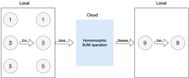
In the worst-case scenario, the cloud service provider cannot be trusted. User data is inherently unsafe if it is in plain text. Even if the service provider is honest, cloud service is prone to fail victims of cybercrime. Security loopholes or sophisticated social engineering attacks expose user privacy on the cloud, and a successful attack usually results in a massive user data leak. One way to eliminate this type of risk is to allow the cloud to operate on the encrypted user data without decrypting it. Fully Homomorphic Encryption (FHE) is a special encryption scheme that allows arbitrary computation over encrypted data without knowing the private key. An FHE enabled cloud service model shown in Fig. 1. In this example, the user wants to compute the sum of 1, 3, 5 in the cloud. The user first encrypts data with FHE, then sends the cipher (shown in Fig. 1 as bubbles with blurry text) to the cloud. When the cloud receives encrypted data, it homomorphically adds all encrypted data together to form an encrypted sum and returns the encrypted sum to the user. The user decrypts the encrypted sum with a secret key, and the result in cleartext is 9 - the sum of 1, 3, and 5. In the entire process, the cloud has no knowledge of user data input and output. Therefore, user data is safe from the insecure cloud or any attack targeted at the cloud service provider.
Fig. 1: Homomorphic Encryption
<details>
<summary>Image 1 Details</summary>
### Visual Description
## Diagram: Homomorphic Encryption Process
### Overview
The image illustrates a homomorphic encryption process involving local computations, encryption, sending data to the cloud for a SUM operation, receiving the result, and decryption back to a local environment.
### Components/Axes
* **Local (Left)**: Represents a local computing environment. Contains three numerical values (1, 3, 5) represented in circles. These values are then encrypted, resulting in blurred versions of the same numbers. An arrow labeled "Enc" indicates the encryption process. An arrow labeled "Send" indicates the encrypted data is sent to the cloud.
* **Cloud (Center)**: Represents a cloud computing environment. A blue rectangle contains the text "Homomorphic SUM operation," indicating the type of computation performed in the cloud.
* **Local (Right)**: Represents another local computing environment. Receives the result from the cloud via an arrow labeled "Receive". The received value (9) is initially blurred, then decrypted via an arrow labeled "Dec", resulting in a clear numerical value (9).
### Detailed Analysis
* **Local (Left)**:
* Three numerical values are present: 1 (top-left), 3 (middle-left), and 5 (bottom-left).
* These values are encrypted, resulting in blurred versions: 1 (top-right), 3 (middle-right), and 5 (bottom-right).
* The encryption process is indicated by an arrow labeled "Enc" pointing from the original values to their encrypted counterparts.
* The encrypted values are sent to the cloud, indicated by an arrow labeled "Send".
* **Cloud (Center)**:
* The cloud performs a "Homomorphic SUM operation" on the received encrypted data.
* **Local (Right)**:
* The result of the SUM operation (9) is received from the cloud.
* The received value is initially blurred, indicating it is still encrypted.
* The value is decrypted, indicated by an arrow labeled "Dec", resulting in a clear numerical value (9).
### Key Observations
* The diagram demonstrates a process where data is encrypted locally, sent to the cloud for computation, and then decrypted locally.
* The "Homomorphic SUM operation" suggests that the cloud is performing a summation of the encrypted values.
* The initial values (1, 3, 5) sum up to 9, which is the final decrypted value, confirming the SUM operation.
### Interpretation
The diagram illustrates the concept of homomorphic encryption, where computations can be performed on encrypted data without decrypting it first. This allows for secure data processing in untrusted environments like the cloud. The diagram specifically shows a SUM operation, but homomorphic encryption can support other types of computations as well. The process ensures that the data remains confidential throughout the entire process, as it is only decrypted in the trusted local environment.
</details>
Blurry text in the figure denotes encrypted data.
Over the years, the research community has developed various encryption schemes that enable computation over ciphers. TFHE [2] is an open-source FHE library that allows fully homomorphic evaluation on arbitrary Boolean circuits. TFHE library
supports FHE operations on unlimited numbers of logic gates. Using FHE logic gates provided by TFHE, users can build an application-specific FHE circuit to perform arbitrary computations over encrypted data. While TFHE library has a good performance in gate-by-gate FHE evaluation speed and memory usage [3], a rigid logic circuit has reusability and scalability issues for general-purpose computing. Also, evaluating a logic circuit in software is slow. Because bitwise FHE operations on ciphers are about one billion times slower than the same operations on plain text, computation time ramps up as the circuit becomes complex.
Herein, we propose a solution that embraces a different approach that draws on a homomorphic instruction set emulator called CryptoEmu. CryptoEmu supports multiple FHE instructions (ADD, SUB, DIV, etc.). When CryptoEmu decodes an instruction, it invokes a pre-built function, referred as functional unit, to perform an FHE operation on input ciphertext. All functional units are built upon FHE gates from TFHE library, and they are accelerated using parallel computing techniques. During execution, the functional units fully utilize a multi-core processor to achieve an optimal speedup. A user would simply reprogram the FHE assembly code for various applications, while relying on the optimized functional units.
This report is organized as follows. Section 2 provides a primer on homomorphic encryption and summarizes related work. Section 3 introduces TFHE, an open-source library for fully homomorphic encryption. TFHE provides the building blocks for CryptoEmu. Section 4 describes CryptoEmu's general architecture. Section 5 and 6 provide detailed instruction set emulator implementations and gives benchmark results on Euler, a CPU/GPU supercomputer. Section 7 analyzes CryptoEmu's scalability and vulnerability, and compared CryptoEmu with a popular FHE software library, HELib [4]. Conclusions and future directions of investigation/development are provided in Section 8.
## II. BACKGROUND
Homomorphic Encryption. Homomorphic encryption (HE) is an encryption scheme that supports computation on encrypted data and generates an encrypted output. When the encrypted output is decrypted, its value is equal to the result when applying equivalent computation on unencrypted data. HE is formally defined as follows: let Enc () be an HE encryption function, Dec () be an HE decryption function, f () be a function, g () be a homomorphic equivalent of f () , and a and b be input data in plaintext. The following equation holds:
$$f ( a , b ) = D e c \left ( g ( E n c ( a ) , E n c ( b ) ) \right ) .$$
An HE scheme is a partially homomorphic encryption (PHE) scheme if g () supports only either addition or multiplication. An HE scheme is a somewhat homomorphic encryption (SWHE) scheme if a limited number of g () is allowed to be applied to encrypted data. An HE scheme is a fully homomorphic encryption (FHE) scheme if any g () can be applied for an unlimited number of times over encrypted data [5].
The first FHE scheme was proposed by Gentry [6]. In HE schemes, the plaintext is encrypted with Gaussian noise. The noise grows after every homomorphic evaluation until the noise becomes too large for the encryption scheme to work. This is the reason that SWHE only allows a limited number of homomorphic evaluations. Gentry introduced a novel technique called 'bootstrapping' such that a ciphertext can be homomorphically decrypted and homomorphically encrypted with the secret key to reduce Gaussian noise [6], [7]. Building off [6], [8] improved bootstrapping to speedup homomorphic evaluations. The TFHE library based on [3] and [9] is one of the FHE schemes with a fast bootstrapping procedure.
Related work. This project proposed a software-based, multiple-instruction ISA emulator that supports fully homomorphic, general-purpose computation. Several general-purpose HE computer architecture implementations exist in both software and hardware. HELib [10] is an FHE software library the implements the Brakerski-Gentry-Vaikuntanathan (BGV) homomorphic encryption scheme [11]. HELib supports HE arithmetic such as addition, subtraction, multiplication, and data movement operations. HELib can be treated as an assembly language for general-purpose HE computing. Cryptoleq [12] is a softwarebased one-instruction set computer (OISC) emulator for general-purpose HE computing. Cryptoleq uses Paillier partially homomorphic scheme [13] and supports Turing-complete SUBLEQ instruction. HEROIC [14] is another OISC architecture implemented on FPGA, based on Paillier partially homomorphic scheme. Cryptoblaze [15] is a multiple-instruction computer based on non-deterministic Paillier encryption that supports partially homomorphic computation. Cryptoblaze is implemented on the FPGA.
## III. TFHE LIBRARY
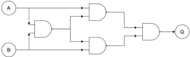
TFHE [2] is an FHE C/C++ software library used to implement fast gate-by-gate bootstrapping. The idea of TFHE is straightforward: if one can homomorphically evaluate a universal logic gate and homomorphically evaluate the next universal logic gate that uses the previous logic gate's output as its input, one can homomorphically evaluate arbitrary Boolean functions, essentially allowing arbitrary FHE computations on encrypted binary data. Figure 2 demonstrates a minimum FHE gate-level library: NAND gate. Bootstrapped NAND gates are used to construct an FHE XOR gate. Similarly, any FHE logic circuit can be constructed with a combination of bootstrapped NAND gates.
Fig. 2: Use of bootstrapped NAND gate to form arbitrary FHE logic circuit. Blurry text in the figure denotes encrypted data.
<details>
<summary>Image 2 Details</summary>
### Visual Description
## Logic Diagram: Complex AND Gate Circuit
### Overview
The image depicts a logic circuit diagram composed of AND gates. The circuit takes two inputs, A and B, and produces a single output, Q. The diagram shows the arrangement of the AND gates and the flow of signals through the circuit.
### Components/Axes
* **Inputs:**
* A (top-left)
* B (bottom-left)
* **Output:**
* Q (right)
* **Logic Gates:** The diagram contains four AND gates.
* **Flow Direction:** The arrows indicate the direction of signal flow from left to right.
### Detailed Analysis
1. **Input A:** The input A is fed directly into the top AND gate on the right side of the diagram. It is also fed into an AND gate on the left side of the diagram.
2. **Input B:** The input B is fed directly into the bottom AND gate on the right side of the diagram. It is also fed into the AND gate on the left side of the diagram.
3. **Left AND Gate:** The inputs A and B are fed into the left AND gate. The output of this AND gate is then fed into both the top and bottom AND gates on the right side of the diagram.
4. **Top Right AND Gate:** This AND gate takes input A and the output of the left AND gate.
5. **Bottom Right AND Gate:** This AND gate takes input B and the output of the left AND gate.
6. **Output AND Gate:** The outputs of the top and bottom AND gates on the right side of the diagram are fed into the final AND gate, which produces the output Q.
### Key Observations
* The circuit uses multiple AND gates to perform a more complex logical operation.
* The inputs A and B are used directly and also combined through an initial AND gate.
* The output Q is the result of combining the direct inputs with the result of the initial AND operation.
### Interpretation
The diagram represents a complex AND gate circuit. The circuit's logic can be described as follows: The output Q is true if and only if both (A AND B) AND (A AND B) are true. The initial AND gate combines A and B, and this result is then used in conjunction with the original A and B inputs in the subsequent AND gates. The final AND gate combines the outputs of these intermediate AND gates to produce the final output Q. This circuit effectively implements a more complex logical function than a simple AND gate.
</details>
TFHE API. TFHE library contains a comprehensive gate bootstrapping API for the FHE scheme [2], including secret-keyset and cloud-keyset generation; Encryption/decryption with secret-keyset; and FHE evaluation on a binary gate netlist with cloudkeyset. TFHE API's performance is evaluated on a single core of Intel Xeon CPU E5-2650 v3 @ 2.30GHz CPU, running CentOS Linux release 8.2.2004 with 128 GB memory. Table I shows the benchmark result of TFHE APIs that are critical to CryptoEmu's performance. TFHE gate bootstrapping parameter setup, Secret-keyset, and cloud-keyset generation are not included in the table.
TABLE I: TFHE API Benchmark
| API | Category | Bootstrapped? | Latency (ms) |
|-----------------|------------------------|-----------------|----------------|
| Encrypt | Encrypt decrypt | N/A | 0.0343745 |
| Decrypt | Encrypt decrypt | N/A | 0.000319556 |
| CONSTANT | Homomorphic operations | No | 0.00433995 |
| NOT | Homomorphic operations | No | 0.000679717 |
| COPY | Homomorphic operations | No | 0.000624117 |
| NAND | Homomorphic operations | Yes | 25.5738 |
| OR | Homomorphic operations | Yes | 25.618 |
| AND | Homomorphic operations | Yes | 25.6176 |
| XOR | Homomorphic operations | Yes | 25.6526 |
| XNOR | Homomorphic operations | Yes | 25.795 |
| NOR | Homomorphic operations | Yes | 25.6265 |
| ANDNY | Homomorphic operations | Yes | 25.6982 |
| ANDYN | Homomorphic operations | Yes | 25.684 |
| ORNY | Homomorphic operations | Yes | 25.7787 |
| ORYN | Homomorphic operations | Yes | 25.6957 |
| MUX | Homomorphic operations | Yes | 49.2645 |
| CreateBitCipher | Ciphertexts | N/A | 0.001725 |
| DeleteBitCipher | Ciphertexts | N/A | 0.002228 |
| ReadBitFromFile | Ciphertexts | N/A | 0.0175304 |
| WriteBitToFile | Ciphertexts | N/A | 0.00960664 |
In Table I, outside the 'Homomorphic operations' category, all other operations are relatively fast. In general, the latency is around 25ms, with exceptions of MUX that takes around 50ms, and CONSTANT, NOT, COPY that are relatively fast. The difference in speed is from gate bootstrapping. Unary gates like CONSTANT, NOT and COPY do not need to be bootstrapped. Binary gates need to be bootstrapped once. MUX needs to be bootstrapped twice. The bootstrapping procedure is manifestly the most computationally expensive operation in TFHE. This overhead is alleviated in CryptoEmu via parallel computing as detailed below.
## IV. CRYPTOEMU ARCHITECTURE OVERVIEW
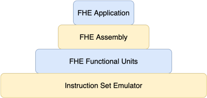
CryptoEmu is a C/C++ utility that emulates the behavior of Fully Homomorphic Encryption (FHE) instructions. The instruction set that CryptoEmu supports is a subset of ARMv8 A32 instructions for fully homomorphic computation over encrypted data. Figure 3 shows the abstract layer for an FHE application. For an FHE application that performs computation over encrypted data, the application will be compiled into FHE assembly that the instruction emulator supports. The instruction set emulator coordinates control units and functional units to decode and execute FHE assembly and returns final results. The design and implementation of CryptoEmu are anchored by two assumptions:
Assumption 1. The instruction set emulator runs on a high-performance multi-core machine.
Assumption 2. The cloud service provider is honest. However, the cloud is subject to cyber-attacks on the user's data.
In §VII-C we will discuss modification on CryptoEmu's implementation when Assumption 2 does not hold.
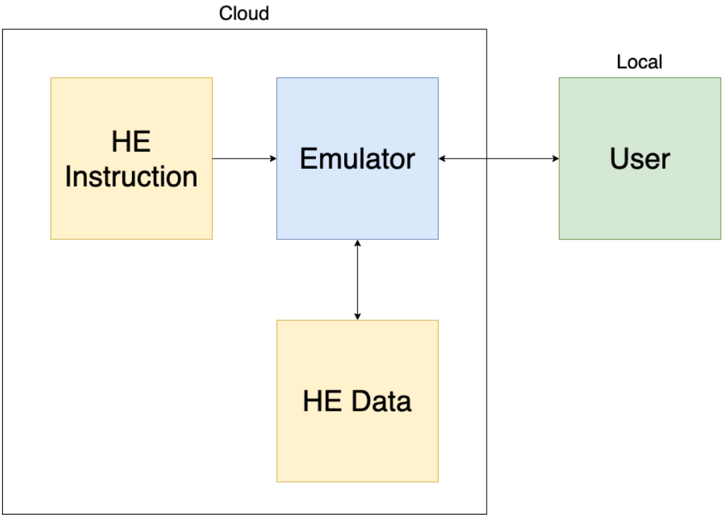
Cloud service model. Figure 4 shows the cloud service model. The instruction set emulator does what an actual hardware asset for encrypted execution would do: it reads from an unencrypted memory space an HE instruction ; i.e., it fetches
Fig. 3: Abstract Layers
<details>
<summary>Image 3 Details</summary>
### Visual Description
## Diagram: FHE Abstraction Layers
### Overview
The image is a diagram illustrating the abstraction layers of a Fully Homomorphic Encryption (FHE) system. It presents a layered structure, resembling a pyramid, with each layer representing a different level of abstraction in the FHE stack.
### Components/Axes
The diagram consists of four rectangular blocks stacked vertically, each representing a different layer. The layers are:
1. **FHE Application** (Top, light blue)
2. **FHE Assembly** (Second from top, light yellow)
3. **FHE Functional Units** (Third from top, light blue)
4. **Instruction Set Emulator** (Bottom, light yellow)
### Detailed Analysis
The diagram shows a hierarchical structure, with the "Instruction Set Emulator" at the base and the "FHE Application" at the top. The blocks are arranged in descending order of size from bottom to top.
* **FHE Application**: The topmost layer, representing the application level that utilizes FHE.
* **FHE Assembly**: The layer below the application, likely representing an assembly-level interface for FHE operations.
* **FHE Functional Units**: The layer below the assembly, representing the fundamental building blocks for FHE computations.
* **Instruction Set Emulator**: The bottom layer, representing the underlying hardware or software that emulates the instruction set required for FHE.
### Key Observations
The diagram visually emphasizes the layered architecture of an FHE system, highlighting the different levels of abstraction involved. The size of each block could be interpreted as representing the complexity or scope of each layer, with the Instruction Set Emulator being the most fundamental and the FHE Application being the most abstract.
### Interpretation
The diagram illustrates the layered approach to building and using FHE systems. It suggests that FHE applications are built on top of lower-level components, such as FHE assembly and functional units, which in turn rely on an instruction set emulator. This layered architecture allows developers to work at different levels of abstraction, depending on their needs and expertise. The diagram implies that the complexity of FHE is managed through this layered approach, making it more accessible to application developers.
</details>
instruction that needs to be executed. The instruction set emulator also reads and writes HE data from an encrypted memory space, to process the user's data and return encrypted results to the encrypted memory space. The user, or any device that owns the user's secret key, will communicate with the cloud through an encrypted channel. The user provides all encrypted data to cloud. The user can send unencrypted HE instructions to the cloud through a secure channel. The user is also responsible for resolving branch directions for the cloud, based on the encrypted branch taken/non-taken result provided by the cloud.
Fig. 4: Cloud service model
<details>
<summary>Image 4 Details</summary>
### Visual Description
## System Diagram: HE Instruction and Data Flow
### Overview
The image is a system diagram illustrating the flow of Homomorphic Encryption (HE) instructions and data between a user, an emulator, and cloud storage. The diagram highlights the interaction between local and cloud-based components.
### Components/Axes
* **Cloud:** A rectangular box encompassing "HE Instruction", "Emulator", and "HE Data".
* **Local:** A label indicating the location of the "User" component.
* **HE Instruction:** A yellow rectangle labeled "HE Instruction".
* **Emulator:** A blue rectangle labeled "Emulator".
* **HE Data:** A yellow rectangle labeled "HE Data".
* **User:** A green rectangle labeled "User".
* **Arrows:** Indicate the direction of data flow between components.
### Detailed Analysis
* **HE Instruction:** Located within the "Cloud" boundary, on the left side. An arrow points from "HE Instruction" to "Emulator".
* **Emulator:** Located within the "Cloud" boundary, in the center. Arrows point to and from "HE Instruction", "HE Data", and "User".
* **HE Data:** Located within the "Cloud" boundary, below the "Emulator". An arrow points from "Emulator" to "HE Data".
* **User:** Located outside the "Cloud" boundary, on the right side, labeled as "Local". An arrow points from "User" to "Emulator" and from "Emulator" to "User".
### Key Observations
* The "Emulator" acts as a central hub, interacting with all other components.
* "HE Instruction" and "HE Data" are both located within the "Cloud".
* The "User" is located "Local" and interacts with the "Emulator" in the "Cloud".
### Interpretation
The diagram depicts a system where a user interacts with an emulator hosted in the cloud. The emulator processes homomorphic encryption instructions and data, likely for secure computation or storage. The user's interaction with the emulator suggests a scenario where data is processed in the cloud without being decrypted, maintaining privacy. The cloud contains the HE Instruction and HE Data, while the user is local.
</details>
## A. Data Processing
In actuality, the HE instruction and HE data can be text files or arrays of data bits stored in buffers, if sufficient memory is available. CryptoEmu employs a load-store architecture. All computations occur on virtual registers (vReg), where a vReg is an array of 32 encrypted data bits. Depending on the memory available on the machine, the number of total vReg is configurable. However, it is the compiler's responsibility to recycle vRegs and properly generate read/write addresses. A snippet of possible machine instructions is as follows:
LOAD R1
```
READ_ADDR1
READ_ADDR2
```
LOAD R2
```
ADD R0 R1, R2
STORE R0 WRITE_ADDR
```
Above, to perform a homomorphic addition, CryptoEmu fetches the LOAD instruction from the instruction memory. Because the instruction itself is in cleartext, CryptoEmu decodes the instruction, loads a piece of encrypted data from HE data memory indexed by READ ADDR1, and copies the encrypted data into vReg R1. Then, CryptoEmu increments its program counter by 4 bytes, reads the next LOAD instruction, and loads encrypted data from HE data memory into vReg R2. After the two operands are ready, CryptoEmu invokes a 32-bit adder and passes R1, R2 to it. The adder returns encrypted data in R0. Finally, CryptoEmu invokes the STORE operation and writes R0 data into the HE data memory pointed to by WRITE ADDR. Under Assumption 2, the honest cloud could infer some user information from program execution because HE instructions are in cleartext. However, all user data stays encrypted and protected from malicious attackers. Vulnerabilities are discussed in §VII-C.
## B. Branch and Control Flow
CryptoEmu can perform a homomorphic comparison and generate N (negative), Z (zero), C (Unsigned overflow), and V (signed overflow) conditional flags. Based on conditional flags, the branch instruction changes the value of the program counter and therefore changes program flow. Because branches are homomorphically evaluated on the encrypted conditional flag, the branch direction is also encrypted. To solve this problem, CryptoEmu employs a client-server communication model from CryptoBlaze [15]. Through a secure communication channel, the cloud server will send an encrypted branch decision to a machine (client) that owns the user's private key. The client deciphers the encrypted branch decision and sends the branch decision encrypted with the server's public key to the server. The cloud server finally decrypts the branch decision, and CryptoEmu will move forward with a branch direction. Under assumption 2, the honest cloud will not use branch decision query and binary search to crack user's encrypted data, nor will the honest cloud infer user information from the user. In §VII-C, the scenario that assumption 2 does not hold will be discussed.
## V. DATA PROCESSING UNITS
Data processing units are subroutines that perform manipulation on encrypted data, including homomorphic binary arithmetic, homomorphic bitwise operation, and data movement. Under Assumption 1, data processing units are implemented with OpenMP [16] and are designed for parallel computing. If the data processing units exhaust all cores available, the rest of the operations will be serialized. We benchmarked the performance of data processing units with 16-bit and 32-bit vReg size. Benchmarks are based an computing node on Euler. The computing node has 2 NUMA nodes. Each NUMA nodes has two sockets, and each socket has a 12-core Intel Xeon CPU E5-2650 v3 @ 2.30GHz CPU. The 48-core computing node runs CentOS Linux release 8.2.2004 with 128 GB memory.
## A. Load/Store Unit
CryptoEmu employs a load/store architecture. A LOAD instruction reads data from data memory; a STORE instruction writes data to data memory. The TFHE library [2] provides the API for load and store operations on FHE data. If data memory is presented as a file, CryptoEmu invokes the specific LD/ST subroutine, moves the file pointer to the right LD/ST address, and calls the appropriate file IO API, i.e.,
```
import_gate_bootstrapping_ciphertext_fromFile()
or
export_gate_bootstrapping_ciphertext_toFile()
```
Preferably, if the machine has available memory, the entire data file is loaded into a buffer as this approach significantly improves LD/ST instruction's performance. Table II shows LD/ST latency for 16-bit and 32-bit. LD/ST on a buffer is significantly faster than LD/ST on a file. The performance speedup is even more when the data file size is large because LD/ST on file needs to use fseek() function to access data at the address specified by HE instructions.
TABLE II: LD/ST latencies.
| | 16-bit (ms) | 32-bit (ms) |
|----------------|---------------|---------------|
| Load (file) | 0.027029 | 0.0554521 |
| Store (file) | 0.0127804 | 0.0276899 |
| Load (buffer) | 0.0043463 | 0.00778488 |
| Store (buffer) | 0.0043381 | 0.0077692 |
```
#pragma omp parallel sections num_threads(2)
{
#pragma omp section
{
bootsAND(&g_o[0], &a_i[0], &b_i[0], bk);
}
#pragma omp section
{
bootsXOR(&p_o[0], &a_i[0], &b_i[0], bk);
}
}
```
Fig. 5: Parallel optimization for bitwise (g,p) calculation, get gp ()
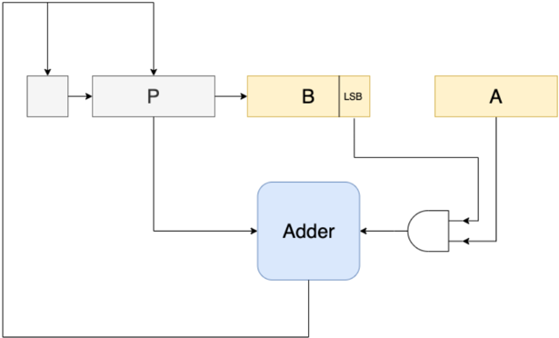
## B. Adder
CryptoEmu supports a configurable adder unit of variable width. As for the ISA that CryptoEmu supports, adders are either 16-bit or 32-bit. Operating under an assumption that CryptoEmu runs on a host that supports multi-threading, the adder unit is implemented as a parallel prefix adder [17]. The parallel prefix adder has a three-stage structure: pre-calculation of generate and propagate bit; carry propagation; and sum computation. Each stage can be divided into sub-stages and can leverage a multi-core processor. Herein, we use the OpenMP [16] library to leverage parallel computing.
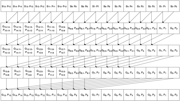
Stage 1: Propagate and generate calculation. Let a and b be the operands to adder, and let a [ i ] and b [ i ] be the i th bit of a and b . In carry-lookahead logic, a [ i ] and b [ i ] generates a carry if a [ i ] AND b [ i ] is 1 and propagates a carry if a [ i ] XOR b [ i ] is 1. This calculation requires an FHE AND gate and an FHE XOR gate, see §III and Fig. 2 for gate bootstrapping. An OpenMP parallel region is created to handle two parallel sections. As shown in Fig. 5, CryptoEmu spawns two threads to execute two OpenMP sections in parallel.
For a 16-bit adder, get gp() calculations are applied on every bit. This process is parallelizable: as shown in Fig. 6, CryptoEmu spawns 16 parallel sections [16], one per bit. Inside each parallel section, the code starts another parallel region that uses two threads. Because of nested parallelism, 32 threads in total are required to calculate every generation and propagate a bit concurrently. If there is an insufficient number of cores, parallel sections will be serialized, which will only affect the efficiency of the emulator.
Stage 2: Carry propagation. Let G i be the carry signal at i th bit, P i be the accumulated propagation bit at i th bit, g i and p i be outputs from propagate and generate calculation. We define operator such that
$$( g _ { x } , p _ { x } ) \odot ( g _ { y } , p _ { y } ) = ( g _ { x } + p _ { x } \cdot g _ { y } , p _ { x } \cdot p _ { y } ) \, .$$
Carry signal G i and accumulated propagation P i can be recursively defined as
$$( G _ { i } , P _ { i } ) = ( g _ { i } , p _ { i } ) \odot ( G _ { i - 1 } , P _ { i - 1 } ) , w h e r e ( G _ { 0 } , P _ { 0 } ) = ( g _ { 0 } , p _ { 0 } ) \, .$$
The above recursive formula is equivalent to
$$( G _ { i \colon j } , P _ { i \colon j } ) = ( G _ { i \colon n } , G _ { i \colon n } ) \odot ( G _ { m \colon j } , P _ { m \colon j } ) , w h e r e i \geq j a n d m \geq n \, .$$
Therefore, carry propagation can be reduced to a parallel scan problem. In CryptoEmu, we defined a routine, get carry() to perform operation . As shown in Fig. 7 , the requires two FHE AND gate and an FHE OR gate. CryptoEmu spawns two threads to perform the operation in parallel.
For a 16-bit adder, we need 4 levels to compute the carry out from the most significant bit. As shown in fig 8, every two arrows that share an arrowhead represents one operation. The operations at the same level can be executed in parallel. In the case of a 16-bit adder, the maximum number of concurrent is 15 at level 1. Because of nested parallelism within the operation, the maximum number of threads required is 30. With a sufficient number of cores, parallel scan reduced carry propagation time from 16 times operation latency, to 4 times operation latency.
Stage 3: Sum calculation. The last stage for parallel prefix adder is sum calculation. Let s i be the sum bit at i th bit, p i be the propagation bit at i th bit, G i be the carry signal at i th bit. Then
$$s _ { i } = p _ { i } \, X O R \, G _ { i } \, .$$
One FHE XOR gate is needed to calculate 1-bit sum. For 16-bit adder, 16 FHE XOR gates are needed. All FHE XOR evaluation are independent, therefore can be executed in parallel. In total 16 threads are required for the best parallel optimization on sum calculation stage.
```
<loc_66><loc_61><loc_379><loc_273><_C++_>#pragma omp parallel sections num_threads(N)
{
#pragma omp section
{
get_gp(&g[0], &p[0], &a[0], &b[0], bk);
}
#pragma omp section
{
get_gp(&g[1], &p[1], &a[1], &b[1], bk);
}
...
#pragma omp section
{
get_gp(&g[14], &p[14], &a[14], &b[14], bk);
}
#pragma omp section
{
get_gp(&g[15], &p[15], &a[15], &b[15], bk);
}
}
```
Fig. 7: Parallel optimization for bitwise carry calculation, get carry ()
a) Benchmark: the 16-bit adder.: Table III shows benchmarking results for a 16-bit adder unit executed on the target machine describe earlier in the document. If parallelized, the 1-bit get gp() shown in Fig. 5 has one FHE gate latency around 25ms as shown in Table I. Ideally, if sufficient cores are available and there is no overhead from parallel optimization, (g,p) calculation should run 16 get gp() concurrently, and total latency should be 25ms. In reality, 16-bit (g,p) calculation uses 32 threads and takes 51.39ms to complete due to overhead in parallel computing.
For carry propagation calculation, the 1-bit get carry() shown in Fig. 7 has two FHE gate latency of around 50ms when parallelized. In an ideal scenario, each level for carry propagation should run get carry() in parallel, and total latency should be around 50ms. In reality, the 16-bit carry propagation calculation uses 30 threads on level 1 and takes 93.42ms. A collection of 28 threads are used on carry propagation level 2; the operation takes 93.58ms. A collection of 24 threads are used on carry propagation level 3; the operation takes 80.34ms. Finally, 16 threads are used on carry propagation level 4; the operation takes 70.85ms.
Fig. 8: Parallel scan for carry signals
<details>
<summary>Image 5 Details</summary>
### Visual Description
## Carry Lookahead Adder Diagram
### Overview
The image is a schematic diagram illustrating the structure of a carry-lookahead adder. It shows the propagation and generation of carry signals across multiple stages of addition. The diagram uses blocks to represent the generation and propagation of carry signals, and arrows to indicate the flow of these signals.
### Components/Axes
The diagram consists of several rows of blocks, each representing a stage in the carry-lookahead adder. Each block contains two variables, G and P, representing the generate and propagate signals, respectively. The subscripts indicate the bit positions involved in the calculation. Arrows connect the blocks, showing the flow of carry signals.
* **Blocks:** Each block contains "G" and "P" values, representing carry generate and propagate signals. The subscripts indicate the bit positions involved.
* **Arrows:** Arrows indicate the flow of carry signals between blocks.
* **Rows:** The diagram has 5 rows, each representing a stage of carry generation and propagation.
### Detailed Analysis or ### Content Details
**Row 1:**
* The first row contains blocks labeled as "G15, P15" to "G0, P0".
* The blocks are arranged horizontally from left to right.
* The subscripts decrease from 15 to 0.
**Row 2:**
* The second row contains blocks labeled as "G15:14, P15:14" to "G0, P0".
* The blocks are arranged horizontally from left to right.
* The subscripts decrease from 15:14 to 0.
* Arrows connect each block in the first row to a block in the second row. The arrows point diagonally downwards and to the right.
**Row 3:**
* The third row contains blocks labeled as "G15:12, P15:12" to "G0, P0".
* The blocks are arranged horizontally from left to right.
* The subscripts decrease from 15:12 to 0.
* Arrows connect each block in the second row to a block in the third row. The arrows point diagonally downwards and to the right.
**Row 4:**
* The fourth row contains blocks labeled as "G15:8, P15:8" to "G0, P0".
* The blocks are arranged horizontally from left to right.
* The subscripts decrease from 15:8 to 0.
* Arrows connect each block in the third row to a block in the fourth row. The arrows point diagonally downwards and to the right.
**Row 5:**
* The fifth row contains blocks labeled as "G15, P15" to "G0, P0".
* The blocks are arranged horizontally from left to right.
* The subscripts decrease from 15 to 0.
* Arrows connect each block in the fourth row to a block in the fifth row. The arrows point downwards.
**Specific Block Labels:**
* Row 1: G15, P15; G14, P14; G13, P13; G12, P12; G11, P11; G10, P10; G9, P9; G8, P8; G7, P7; G6, P6; G5, P5; G4, P4; G3, P3; G2, P2; G1, P1; G0, P0
* Row 2: G15:14, P15:14; G14:13, P14:13; G13:12, P13:12; G12:11, P12:11; G11:10, P11:10; G10:9, P10:9; G9:8, P9:8; G8:7, P8:7; G7:6, P7:6; G6:5, P6:5; G5:4, P5:4; G4:3, P4:3; G3:2, P3:2; G2:1, P2:1; G1, P1; G0, P0
* Row 3: G15:12, P15:12; G14:11, P14:11; G13:10, P13:10; G12:9, P12:9; G11:8, P11:8; G10:7, P10:7; G9:6, P9:6; G8:5, P8:5; G7:4, P7:4; G6:3, P6:3; G5:2, P5:2; G4:1, P4:1; G3, P3; G2, P2; G1, P1; G0, P0
* Row 4: G15:8, P15:8; G14:7, P14:7; G13:6, P13:6; G12:5, P12:5; G11:4, P11:4; G10:3, P10:3; G9:2, P9:2; G8:1, P8:1; G7, P7; G6, P6; G5, P5; G4, P4; G3, P3; G2, P2; G1, P1; G0, P0
* Row 5: G15, P15; G14, P14; G13, P13; G12, P12; G11, P11; G10, P10; G9, P9; G8, P8; G7, P7; G6, P6; G5, P5; G4, P4; G3, P3; G2, P2; G1, P1; G0, P0
### Key Observations
* The diagram illustrates a hierarchical structure for carry generation and propagation.
* The carry signals are combined across multiple bit positions in each stage.
* The final row represents the carry signals for each bit position.
### Interpretation
The diagram shows the architecture of a carry-lookahead adder, which is a type of adder used in digital circuits to improve speed by reducing the delay associated with carry propagation. The diagram illustrates how carry signals are generated and propagated across multiple stages, allowing for faster addition compared to ripple-carry adders. The hierarchical structure allows for parallel computation of carry signals, which significantly reduces the overall addition time.
</details>
TABLE III: 16-bit adder latency
<details>
<summary>Image 6 Details</summary>
### Visual Description
## Data Table: Operation Latency
### Overview
The image presents a data table showing the latency (in milliseconds) for different operations. The operations include (g,p) calculation, carry propagation at four levels, sum calculation, and total latency including overhead.
### Components/Axes
* **Columns:** The table has two columns: "Operation" and "Latency (ms)".
* **Rows:** Each row represents a specific operation and its corresponding latency.
### Detailed Analysis
Here's a breakdown of the data:
| Operation | Latency (ms) |
| ------------------------------- | ------------- |
| (g,p) calculation | 51.3939 |
| Carry propagation (Level 1) | 93.4178 |
| Carry propagation (Level 2) | 93.5273 |
| Carry propagation (Level 3) | 80.342 |
| Carry propagation (Level 4) | 70.8481 |
| Sum calculation | 34.2846 |
| Total latency, including overhead | 528.482 |
* **(g,p) calculation:** 51.3939 ms
* **Carry propagation (Level 1):** 93.4178 ms
* **Carry propagation (Level 2):** 93.5273 ms
* **Carry propagation (Level 3):** 80.342 ms
* **Carry propagation (Level 4):** 70.8481 ms
* **Sum calculation:** 34.2846 ms
* **Total latency, including overhead:** 528.482 ms
### Key Observations
* Carry propagation at levels 1 and 2 have the highest individual latencies among the listed operations.
* The total latency, including overhead, is significantly higher than the sum of the individual operation latencies, indicating a substantial overhead component.
* The latency of carry propagation decreases as the level increases from 2 to 4.
### Interpretation
The data suggests that carry propagation is a significant bottleneck in the overall process, especially at the initial levels (1 and 2). The substantial difference between the sum of individual operation latencies and the total latency indicates that overhead contributes significantly to the overall processing time. The decreasing latency in carry propagation from level 2 to 4 may indicate optimizations or reduced complexity at higher levels.
</details>
| Operation | Latency (ms) |
|-----------------------------------|----------------|
| (g,p) calculation | 51.3939 |
| Carry propagation (Level 1) | 93.4178 |
| Carry propagation (Level 2) | 93.5273 |
| Carry propagation (Level 3) | 80.342 |
| Carry propagation (Level 4) | 70.8481 |
| Sum calculation | 34.2846 |
| Total latency, including overhead | 528.482 |
For sum calculation, 1-bit sum calculation uses one FHE XOR gate, with latency around 25ms. Ideally, if CryptoEmu runs all 16 XOR gates in parallel without parallel computing overhead, the latency for 16-bit sum calculation should be around 25ms. In reality, due to OpenMP overhead, the 16-bit sum calculation uses 16 threads and takes 34.28ms to complete.
In total, a 16-bit adder's latency is 486.66ms. This result includes latency for all stages, plus overheads like variable declaration, memory allocation, and temporary variable manipulation.
b) Benchmark: the 32-bit adder.: Table IV shows benchmarking results for a 32-bit adder unit executed on the target machine describe earlier in the document. Note that get gp() and get carry() have the same performance as the 16-bit adder. If sufficient cores are available, in the absence of OpenMP overhead, the (g,p) calculation should run 32 get gp() concurrently for 32-bit adder at a total latency of 25ms. In reality, the 32-bit (g,p) calculation uses 32 threads and takes 94.92ms to complete.
TABLE IV: 32-bit adder latency
| Operation | Latency (ms) |
|-----------------------------------|----------------|
| (g,p) calculation | 94.9246 |
| Carry propagation (Level 1) | 147.451 |
| Carry propagation (Level 2) | 133.389 |
| Carry propagation (Level 3) | 127.331 |
| Carry propagation (Level 4) | 112.268 |
| Carry propagation (Level 5) | 91.5781 |
| Sum calculation | 49.0098 |
| Total latency, including overhead | 941.12 |
For carry propagation calculation, if sufficient cores are available, each level for carry propagation should run get carry() in parallel. Without parallel computing overhead, total latency should be around 50ms. Level 0 of 32-bit carry propagation calculation uses 62 threads. Because the platform on which CryptoEmu is tested has only 48 cores, level 0 carry propagation calculation is serialized and takes 147.45ms to complete. Level 1 carry propagation calculation uses 60 threads, and similar to level 0, its calculation is serialized. Level 1 carry propagation calculation takes 133.39ms. Level 3 carry propagation calculation that uses 56 threads is serialized and takes 127.33ms to complete. Level 4 carry propagation calculation uses 48 threads, and it is possible to run every get carry() in parallel on our 48-core workstation. Level 4 carry propagation calculation takes 112.27ms. Level 5 carry propagation calculation uses 32 threads. It is able to execute all get carry() concurrently; level 5 takes 91.58ms to complete.
For sum calculation, the 32-bit adder spawns 32 threads in parallel to perform FHE XOR operation if sufficient cores are available. The latency for the 32-bit sum calculation should be around 25ms. In reality, the 32-bit sum calculation uses 32 threads and takes 49ms to complete.
In total, 32-bit adder's latency is 941.12ms. This result includes latency for all stages, plus overheads like variable declaration, memory allocation, and temporary variable manipulation.
## C. Subtractor
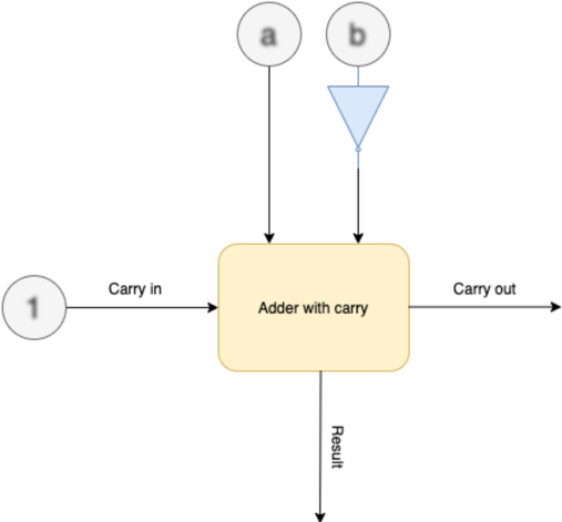
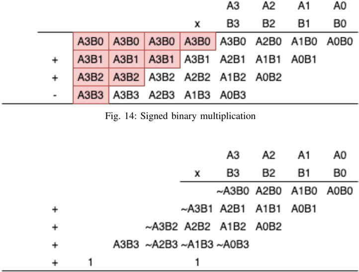
The subtractor unit supports variable ALU size. CryptoEmu supports subtractors with 16-bit operands or 32-bit operands. Let a be the minuend, b be the subtrahend, and diff be the difference. Formula for 2's complement subtraction is:
$$a + N O T ( b ) + 1 = d i f f \, .$$
As shown in Fig. 9, CryptoEmu reuses adder units in §V-B to perform homomorphic subtractions. On the critical path, extra homomorphic NOT gates are used to create subtrahend's complement. For a subtractor with N-bit operands, N homomorphic NOT operations need to be applied on the subtrahend. While all FHE NOT gates can be evaluated in parallel, in §III we showed that FHE NOT gates do not need bootstrapping, and is relatively fast (around 0.0007ms latency per gate) comparing to bootstrapped FHE gates. Therefore, parallel execution is not necessary. Instead, the homomorphic NOT operation is implemented in an iterative for-loop, as shown below:
$$\begin{array} { r l } & { f o r ( i n t \, i = 0 ; \, i < N ; \, + + i ) } \\ & { b o o t s N O T ( \& b _ { - } n e g [ i ] , \, & b k [ i ] , \, b k ) ; } \end{array}$$
In addition to homomorphic NOT operation on subtrahend, the carry out bit from bit 0 needs to be evaluated with an OR gate because carry in is 1. Therefore, the adder in §V-B is extended to take a carry in bit. When sufficient cores are available on the machine, a subtractor units adds negation and carry bit calculation to the adder unit's critical path.
Fig. 9: Subtractor architecture. Blurry text in the figure denotes encrypted data.
<details>
<summary>Image 7 Details</summary>
### Visual Description
## Diagram: Adder with Carry
### Overview
The image is a diagram of an adder with carry, illustrating the inputs and outputs of the adder. The diagram shows the flow of data into and out of the adder, including carry-in, carry-out, and the result.
### Components/Axes
* **Inputs:**
* 'a' - Input 'a' to the adder. Represented by a circle with the letter 'a' inside.
* 'b' - Input 'b' to the adder. Represented by a circle with the letter 'b' inside, connected to a blue triangle pointing downwards.
* 'Carry in' - Carry-in input to the adder. Represented by a circle with the number '1' inside.
* **Process:**
* 'Adder with carry' - The main processing block, represented by a yellow rounded rectangle.
* **Outputs:**
* 'Carry out' - Carry-out output from the adder.
* 'Result' - The result of the addition.
### Detailed Analysis
* The diagram shows three inputs to the "Adder with carry" block: 'a', 'b', and 'Carry in'.
* The 'a' input comes directly from a source labeled 'a'.
* The 'b' input comes from a source labeled 'b', which is connected to a blue triangle pointing downwards.
* The 'Carry in' input comes from a source labeled '1'.
* The "Adder with carry" block has two outputs: 'Carry out' and 'Result'.
* The 'Carry out' output goes to the right.
* The 'Result' output goes downwards.
### Key Observations
* The diagram illustrates the basic components and flow of data in an adder with carry.
* The blue triangle pointing downwards connected to 'b' is likely an inverter.
### Interpretation
The diagram represents a full adder circuit. The 'a' and 'b' inputs are the two numbers being added. The 'Carry in' input is the carry from the previous stage of addition. The 'Adder with carry' block performs the addition and generates two outputs: the 'Result' (sum) and the 'Carry out' (carry to the next stage). The blue triangle pointing downwards connected to 'b' likely represents an inverter, suggesting that the 'b' input might be inverted before being fed into the adder.
</details>
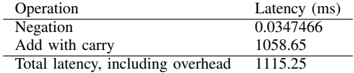
a) Benchmark.: Tables V and VI report benchmark results for the 16-bit and 32-bit subtractors on the target machine. Negation on the subtrahend takes a trivial amount of time to complete. The homomorphic addition is the most time-consuming operation in the subtractor unit. The homomorphic addition is a little slower than the homomorphic additions in §V-B because the adder needs to use extra bootstrapped FHE gates to process carry in and calculate carry out from sum bit 0.
TABLE V: 16-bit subtractor latency
<details>
<summary>Image 8 Details</summary>
### Visual Description
## Data Table: Operation Latency
### Overview
The image presents a data table showing the latency of different operations, measured in milliseconds (ms). The table includes the latency for "Negation", "Add with carry", and the "Total latency, including overhead".
### Components/Axes
* **Columns:**
* Operation
* Latency (ms)
* **Rows:**
* Negation
* Add with carry
* Total latency, including overhead
### Detailed Analysis or ### Content Details
| Operation | Latency (ms) |
| ------------------------------- | ------------ |
| Negation | 0.0341106 |
| Add with carry | 680.59 |
| Total latency, including overhead | 715.015 |
### Key Observations
* The "Add with carry" operation has a significantly higher latency (680.59 ms) compared to the "Negation" operation (0.0341106 ms).
* The "Total latency, including overhead" (715.015 ms) is greater than the "Add with carry" latency, indicating that the overhead and negation latency contribute to the total latency.
### Interpretation
The data suggests that the "Add with carry" operation is the most time-consuming operation in this context. The total latency is only slightly higher than the "Add with carry" latency, implying that the overhead and negation operations contribute a relatively small amount to the overall latency. The table highlights the performance bottleneck associated with the "Add with carry" operation.
</details>
| Operation | Latency (ms) |
|-----------------------------------|----------------|
| Negation | 0.0341106 |
| Add with carry | 680.59 |
| Total latency, including overhead | 715.015 |
## D. Shifter
CryptoEmu supports three types of shifters: logic left shift (LLS), logic right shift (LRS), and arithmetic right shift (ARS). Each shifter type has two modes: immediate and register mode. In immediate mode, the shift amount is in cleartext. For example, the following instruction shifts encrypted data in R0 to left by 1 bit and assigns the shifted value to R0.
<details>
<summary>Image 9 Details</summary>

### Visual Description
Icon/Small Image (238x17)
</details>
This instruction is usually issued by the cloud to process user data. Shift immediate implementation is trivial. The shifter calls bootCOPY() API to move all data to the input direction by the specified amount. The LSB or MSB will be assigned to an encrypted constant using the bootCONSTANT() API call. Because neither bootCOPY() nor bootCONSTANT() need to be bootstrapped, they are fast operations, see Table III. Therefore, an iterative loop is used for shifting. Parallel optimization is unnecessary.
In register mode, the shift amount is an encrypted data stored in the input register. For example, the following instruction shifts encrypted data in R0 to left by the value stored in R1 and assign shifted value to R0.
```
LLS R0 R0 R1
```
Because the shifting amount stored in R1 is encrypted, the shifter can't simply move all encrypted bits left/right by a certain amount. The shifter is implemented as a barrel shifter, with parallel computing enabled.
a) Logic left shift.: Figure 10 shows the architecture for the 16-bit LLS. In the figure, numbers in the bubbles denote encrypted data in the shift register and the shift amount register. Numbers in the diamond denote an encrypted constant value generated by the bootsCONSTANT() API. The 16-bit LLS has four stages. In each stage, based on the encrypted shift amount, the FHE MUX homomorphically selects an encrypted bit from the shift register. In the end, the LLS outputs encrypted shifted data. FHE MUX is an elementary logic unit provided by TFHE library [2]. FHE MUX needs to be bootstrapped twice, and its latency is around 50ms. Therefore, it is reasonable to spawn multiple threads to execute all MUX select in parallel in each stage. For the 16-bit LLS, each stage needs 16 threads to perform a homomorphic MUX select, as shown in the following code:
```
its latency is around 50ms. Therefore, it is reasonable to spawn multiple threads to execute all MUX select stage. For the 16-bit LLS, each stage needs 16 threads to perform a homomorphic MUX select, as show code:
{
#pragma omp parallel sections num_threads(16)
{
#pragma omp section
{
bootsMUX(&out[0], &amt[0], &zero[0], &in[0], bk);
}
#pragma omp section
{
bootsMUX(&out[1], &amt[0], &in[0], &in[1], bk);
}
...
#pragma omp section
{
bootsMUX(&out[14], &amt[0], &in[13], &in[14], bk);
}
#pragma omp section
{
bootsMUX(&out[15], &amt[0], &in[14], &in[15], bk);
}
}
```
TABLE VI: 32-bit subtractor latency
<details>
<summary>Image 10 Details</summary>
### Visual Description
## Table: Operation Latency
### Overview
The image presents a table showing the latency (in milliseconds) for different operations. It includes the latency for negation, addition with carry, and the total latency including overhead.
### Components/Axes
* **Columns:**
* Operation
* Latency (ms)
* **Rows:**
* Negation
* Add with carry
* Total latency, including overhead
### Detailed Analysis
The table provides the following latency values:
* **Negation:** 0.0347466 ms
* **Add with carry:** 1058.65 ms
* **Total latency, including overhead:** 1115.25 ms
### Key Observations
* The "Add with carry" operation has a significantly higher latency compared to "Negation".
* The "Total latency, including overhead" is greater than the "Add with carry" latency, indicating that overhead contributes to the overall latency.
### Interpretation
The data suggests that the "Add with carry" operation is computationally more expensive than "Negation". The difference between the "Total latency" and the "Add with carry" latency (1115.25 - 1058.65 = 56.6 ms) represents the overhead associated with the operations. This overhead could include factors such as memory access, function call overhead, or other system-level processes. The table highlights the relative performance costs of different operations, which can be useful for optimizing code or hardware designs.
</details>
| Operation | Latency (ms) |
|-----------------------------------|----------------|
| Negation | 0.0347466 |
| Add with carry | 1058.65 |
| Total latency, including overhead | 1115.25 |
Fig. 10: LLS architecture
<details>
<summary>Image 11 Details</summary>
### Visual Description
## Diagram: Barrel Shifter Architecture
### Overview
The image depicts a barrel shifter architecture, a digital circuit that can shift a data word by a specified number of bits without using any sequential logic, only combinational logic. The diagram shows a 16-bit barrel shifter implemented using multiple stages of multiplexers (Mux). The shift amount is controlled by the input at the bottom, and the output is the shifted data at the top.
### Components/Axes
* **Shift Reg:** (Shift Register) - Labeled on the top-left. Represents the input data to be shifted. Values range from 0 to 15, arranged vertically.
* **Output:** Labeled on the top-right. Represents the output data after shifting. Values range from 0 to 15, arranged vertically.
* **Shift Amount:** Labeled on the bottom-left. Represents the amount by which the input data is shifted. Values range from 0 to 3, arranged vertically.
* **Mux:** (Multiplexer) - Labeled on each multiplexer component.
* **Diamonds with "0":** These represent a constant input of 0 to the multiplexers.
### Detailed Analysis
The diagram consists of several columns of multiplexers. Each multiplexer selects between two inputs based on the shift amount. The shift amount inputs (0-3) control the selection of the multiplexers in each stage.
* **Input Stage (Shift Reg):** The input data is labeled from 0 to 15, arranged vertically on the left side. Each input is connected to the first column of multiplexers.
* **Multiplexer Stages:** There are multiple columns of multiplexers. Each multiplexer has two inputs: one from the previous stage and one from a shifted position. The shift amount determines which input is selected.
* **Shift Amount Control:** The shift amount inputs (0, 1, 2, 3) at the bottom control the selection of the multiplexers in each stage. The diamond shapes with "0" inside represent a constant input of 0 to the multiplexers.
* **Output Stage:** The output data is labeled from 0 to 15, arranged vertically on the right side. Each output is connected to the last column of multiplexers.
**Detailed Connections:**
* **Shift Amount 0:** When the shift amount is 0, the multiplexers select the input directly from the previous stage, resulting in no shift.
* **Shift Amount 1:** When the shift amount is 1, the multiplexers select the input shifted by one position.
* **Shift Amount 2:** When the shift amount is 2, the multiplexers select the input shifted by two positions.
* **Shift Amount 3:** The diagram does not explicitly show the connections for shift amount 3, but it can be inferred that the multiplexers would select the input shifted by three positions.
### Key Observations
* The diagram illustrates a 16-bit barrel shifter architecture.
* The shift amount is controlled by the input at the bottom.
* The output is the shifted data at the top.
* The multiplexers select between two inputs based on the shift amount.
* The diamond shapes with "0" inside represent a constant input of 0 to the multiplexers.
### Interpretation
The barrel shifter architecture allows for efficient shifting of data by a specified number of bits. The multiplexers select between different shifted positions based on the shift amount. This architecture is commonly used in digital circuits for various applications, such as data processing, signal processing, and cryptography. The use of multiplexers allows for a fast and efficient implementation of the shift operation. The diagram provides a clear representation of the barrel shifter architecture and its components.
</details>
In a parallel implementation with zero overhead, each stage should have one FHE MUX latency of around 50ms. Therefore, in an ideal scenario, four stages would have a latency of around 200ms.
b) Benchmark: Logic left shift.: Table VII shows the benchmark results for the 16-bit LLS on the target platform. Each stage spawns 16 threads to run all FHE MUX in parallel with latency from 50-90ms, a latency that is in between 1 FHE MUX latency to 2 FHE MUX latency, due to parallel computing overhead. In total, it takes around 290ms to carry out a homomorphic LLS operation on 16-bit encrypted data.
TABLE VII: 16-bit LLS latency
| Operation | Latency (ms) |
|-----------------------------------|----------------|
| Mux select (Stage 1) | 87.3295 |
| Mux select (Stage 2) | 82.2656 |
| Mux select (Stage 3) | 76.6871 |
| Mux select(Stage 4) | 55.5396 |
| Total latency, including overhead | 287.92 |
Table VIII shows the benchmark result for the 32-bit LLS. Each stage spawns 32 threads and takes around 90-100ms to complete. In total, it takes around 450-500ms for a homomorphic LLS operation on 32-bit encrypted data.
TABLE VIII: 32-bit LLS latency
| Operation | Latency (ms) |
|-----------------------------------|----------------|
| Mux select (Stage 1) | 101.92 |
| Mux select (Stage 2) | 89.7695 |
| Mux select (Stage 3) | 98.8634 |
| Mux select(Stage 4) | 91.3939 |
| Mux select (Stage 5) | 91.8491 |
| Total latency, including overhead | 474.739 |
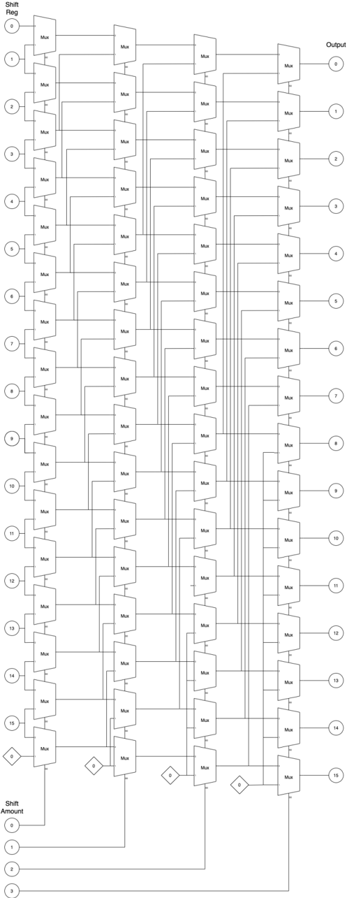
c) Logic right shift/Arithmetic right shift.: LRS has an architecture that is similar to the architecture of LLS. Figure 11 shows the architecture for the 16-bit LRS. Compared to Fig. 10, the only difference between LLS and LRS is the bit order of the input register and output register. To reuse the LRS architecture for ARS, one should simply pass MSB of the shift register as the shift-in value, shown as the numbers in the diamond in Fig. 11. The LRS and ARS shifter implementation is similar to that of LLS. For 16-bit LRS/ARS, CryptoEmu spawns 16 parallel threads to perform a homomorphic MUX select at each stage.
Table IX shows the benchmark result for the 16-bit LRS and ARS. LRS and ARS have similar performance. At each stage, LRS/ARS utilizes 16 threads, and each stage takes 50-90ms to complete. Single stage latency is between 1 FHE MUX latency to 2 FHE MUX latency, due to parallel computing overhead. In total, 16-bit LRS/ARS latency is around 290-300ms.
TABLE IX: 16-bit LRS, ARS latency
| Operation | LRS Latency (ms) | ARS Latency (ms) |
|-----------------------------------|--------------------|--------------------|
| Mux select (Stage 1) | 88.1408 | 87.7689 |
| Mux select (Stage 2) | 85.5154 | 79.6416 |
| Mux select (Stage 3) | 75.0295 | 75.2938 |
| Mux select(Stage 4) | 55.9639 | 54.9246 |
| Total latency, including overhead | 290.517 | 296.124 |
Table X shows the benchmark result for the 32-bit LRS and ARS. The 32-bit LRS/ARS has five stages. Each stage creates 32 parallel threads to evaluate FHE MUX and takes 90-100ms to complete. Single stage latency is around 2 FHE MUX latency. In total, the 32-bit LRS/ARS takes around 470-500ms to complete a homomorphic LRS/ARS operation on 32-bit encrypted data.
TABLE X: 32-bit LRS, ARS latency
| Operation | LRS Latency (ms) | ARS Latency (ms) |
|-----------------------------------|--------------------|--------------------|
| Mux select (Level 1) | 104.33 | 106.132 |
| Mux select (Level 2) | 104.75 | 95.3209 |
| Mux select (Level 3) | 90.2377 | 90.1364 |
| Mux select(Level 4) | 89.7183 | 90.5383 |
| Mux select(Level 5) | 90.6315 | 94.4654 |
| Total latency, including overhead | 472.896 | 491.787 |
Fig. 11: LRS architecture
<details>
<summary>Image 12 Details</summary>
### Visual Description
## Diagram: Barrel Shifter
### Overview
The image is a schematic diagram of a 16-bit barrel shifter implemented using multiplexers (Mux). It shows how the input bits are shifted based on the shift amount. The diagram consists of multiple stages of multiplexers arranged in columns, with connections indicating the data flow for different shift amounts.
### Components/Axes
* **Shift Reg:** (Top-left) Input register with 16 bits, labeled 0 to 15.
* **Output:** (Top-right) Output register with 16 bits, labeled 0 to 15.
* **Mux:** Multiplexer component, repeated throughout the diagram.
* **Shift Amount:** (Bottom-left) Shift amount input, labeled 0 to 3.
* **Diamonds:** Control signals for the multiplexers, labeled "0".
### Detailed Analysis
The diagram shows a multi-stage arrangement of multiplexers. Each stage corresponds to a different power of 2 shift (1, 2, 4, 8).
* **Input (Shift Reg):** The input is a 16-bit register, with each bit labeled from 0 to 15, positioned vertically on the left side of the diagram. Each bit is connected to the first column of multiplexers.
* **Multiplexers (Mux):** The diagram uses multiple columns of multiplexers. Each multiplexer has two inputs and one output. The control signal for each multiplexer determines which input is passed to the output. The multiplexers are arranged in a grid-like structure.
* **Shift Amount:** The shift amount is controlled by the input at the bottom of the diagram, labeled 0 to 3. These inputs control the selection lines of the multiplexers.
* **Control Signals:** The diamond shapes labeled "0" represent control signals that determine the selection of the multiplexers.
* **Output:** The output is a 16-bit register, with each bit labeled from 0 to 15, positioned vertically on the right side of the diagram. Each bit is the output of the last column of multiplexers.
**Data Flow:**
The data flows from left to right. The input bits from the "Shift Reg" are fed into the first column of multiplexers. Based on the "Shift Amount" and the control signals, the multiplexers select the appropriate input and pass it to the next stage. This process continues through each column of multiplexers until the final shifted output is obtained at the "Output" register.
**Specific Connections:**
* The first column of multiplexers takes the input from the "Shift Reg".
* The second column of multiplexers takes the output from the first column.
* The third column of multiplexers takes the output from the second column.
* The fourth column of multiplexers takes the output from the third column.
* The output of the fourth column is the final shifted output.
### Key Observations
* The diagram illustrates a 16-bit barrel shifter.
* The shifter is implemented using multiplexers.
* The shift amount is controlled by the input at the bottom of the diagram.
* The control signals determine the selection of the multiplexers.
* The data flows from left to right through the multiplexer stages.
### Interpretation
The diagram demonstrates how a barrel shifter can be implemented using multiplexers. A barrel shifter is a digital circuit that can shift a data word by a specified number of bits without using any sequential logic, making it faster than shift registers for multi-bit shifts. The arrangement of multiplexers allows for efficient shifting of the input bits based on the shift amount. The control signals determine the specific connections and data flow required to achieve the desired shift. The diagram provides a clear visual representation of the internal workings of a barrel shifter, highlighting the role of multiplexers in achieving the shifting functionality.
</details>
## E. Multiplier
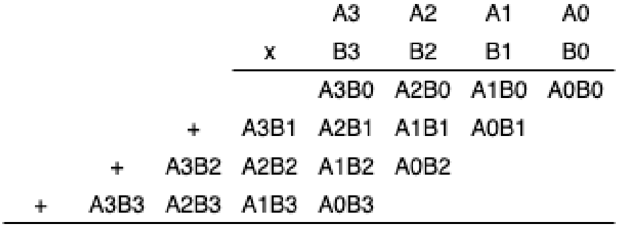
Design consideration. Binary multiplication can be treated as a summation of partial products [18], see Fig. 12. Therefore, adder units mentioned in §V-B can be reused for partial sum computation. Summing up all partial products is a sum reduction operation, and therefore can be parallelized.
Fig. 12: Binary multiplication
<details>
<summary>Image 13 Details</summary>
### Visual Description
## Multiplication Diagram: Binary Multiplication
### Overview
The image depicts the multiplication of two 4-bit binary numbers, A and B, using the standard multiplication algorithm. It shows the partial products generated by multiplying each bit of B with the entire number A, and then summing these partial products to obtain the final result.
### Components/Axes
* **Top Row:** A3, A2, A1, A0 (representing the bits of number A, from most significant to least significant)
* **Second Row:** x, B3, B2, B1, B0 (representing the bits of number B, from most significant to least significant, with 'x' indicating multiplication)
* **Partial Products:**
* A3B0, A2B0, A1B0, A0B0 (A multiplied by B0)
* A3B1, A2B1, A1B1, A0B1 (A multiplied by B1)
* A3B2, A2B2, A1B2, A0B2 (A multiplied by B2)
* A3B3, A2B3, A1B3, A0B3 (A multiplied by B3)
* **'+' signs:** Indicate the addition of the partial products.
### Detailed Analysis or ### Content Details
The diagram illustrates the multiplication process as follows:
1. **First Partial Product:** A is multiplied by B0, resulting in A3B0, A2B0, A1B0, A0B0.
2. **Second Partial Product:** A is multiplied by B1, resulting in A3B1, A2B1, A1B1, A0B1. This partial product is shifted one position to the left.
3. **Third Partial Product:** A is multiplied by B2, resulting in A3B2, A2B2, A1B2, A0B2. This partial product is shifted two positions to the left.
4. **Fourth Partial Product:** A is multiplied by B3, resulting in A3B3, A2B3, A1B3, A0B3. This partial product is shifted three positions to the left.
The '+' signs indicate that these partial products are then added together to obtain the final product.
### Key Observations
* The diagram clearly shows the bitwise multiplication and the necessary left shifts for each partial product.
* The representation uses symbolic notation (A3B0, etc.) to represent the AND operation between the corresponding bits of A and B.
### Interpretation
The diagram demonstrates the standard algorithm for binary multiplication. Each partial product is generated by performing a bitwise AND operation between the bits of the multiplicand (A) and a single bit of the multiplier (B). The partial products are then shifted left by an amount corresponding to the bit position of the multiplier and added together. This process is fundamental to digital arithmetic and is implemented in hardware multipliers within computer systems. The diagram provides a visual representation of this process, making it easier to understand the underlying logic.
</details>
However, the best parallel optimization cannot be achieved on our 48-core computing node. For a 16-bit wide multiplier, the product is a 32-bit encrypted value. Therefore, a 32-bit adder is required to carry out the homomorphic addition. Each 32-bit adder has peak thread usage of 64 threads: 31 threads with nested parallel (g,p) calculation that uses two threads. Thus, on the server used (with 48 cores), the 32-bit adder has to be partially serialized. For the 16-bit multiplier's parallel sum reduction, at most eight summation occur in parallel and each summation uses a 32-bit adder. The peak thread usage is 512 threads. For a 32-bit multiplier, maximum thread usage is 2048 threads. Thus, because homomorphic multiplication is a computationally demanding process, the server used does not have sufficient resources to do all operations in parallel. Homomorphic multiplication will thus show suboptimal performance on the server used in this project.
Based on the design consideration above, CryptoEmu implements a carry-save multiplier [19] that supports variable ALU width. Carry-save multiplier uses an adder described in V-B to sum up partial products in series.
- 1) Unsigned multiplication: Figure 13 shows the multiplier's architecture. For a 16-bit multiplier, A and B are 16-bit operands stored in vRegs. P is an intermediate 16-bit vReg to store partial products. Adder is a 16-bit adder with a carry in bit, see §V-B.
On startup, vReg P is initialized to encrypted 0 using TFHE library's bootCONSTANT() API. Next, we enter an iterative loop and homomorphically AND all bits in vReg A with LSB of vReg B , and use the result as one of the operands to the 16-bit adder. Data stored in vReg P is then passed to the 16-bit adder as the second operand. The adder performs the homomorphic addition to output an encrypted carry out bit. Next, we right shift carry out, vReg P and vReg B , and reached the end of the iterative for-loop. We repeat the for-loop 16 times, and the final product is a 32-bit result stored in vReg P and vReg B . The pseudo-code below shows the 16-bit binary multiplication algorithm.
```
P = 0;
for 16 times:
(P, carry out) = P + (B[0] ? A : 0)
[carry out, P, B] = [carry out, P, B] >> 1;
return [P, B]
```
For implementation, an N-bit multiplier uses N threads to concurrently evaluate all the FHE AND gates. The adder is already parallel optimized. The rest of the multiplication subroutine is executed sequentially. Therefore, the multiplier is a computationally expensive unit in CryptoEmu.
- a) Benchmark: Unsigned multiplication.: Table XI shows benchmark for 16-bit unsigned multiplication and 32-bit unsigned multiplication. A single pass for partial product summation takes around 715ms and 925ms, respectively. Total latency is roughly equal to N times single iteration's latency because summation operations are in sequence.
- 2) Signed multiplication: Signed multiplication is implemented using the carry-save multiplier in Figure 13, with slight modifications. For N-bit signed multiplication, partial products need to be signed extended to 2N bit. Figure 14 shows the partial product summation for 4-bit signed multiplication. This algorithm requires a 2N-bit adder and a 2N-bit subtractor for
TABLE XI: Unsigned multiplication latency
| | 16-bit multiplier (ms) | 32-bit multiplier (ms) |
|-----------------------------------|--------------------------|--------------------------|
| Single iteration | 715.812 | 926.79 |
| Total latency, including overhead | 11316.8 | 36929.2 |
Fig. 13: Carry save multiplier
<details>
<summary>Image 14 Details</summary>
### Visual Description
## Diagram: Data Flow Diagram
### Overview
The image is a data flow diagram illustrating a computational process. It shows several components (registers, adder, AND gate) and the flow of data between them.
### Components/Axes
* **Registers:**
* A (yellow)
* B (yellow)
* P (gray)
* Unnamed register (gray)
* **Adder:** (blue)
* **AND Gate:** (white)
* **LSB:** Label indicating the Least Significant Bit of register B.
### Detailed Analysis or ### Content Details
1. **Data Flow:**
* Data flows from the unnamed register to register P.
* Data flows from register P to register B.
* Data flows from the LSB of register B to the AND gate.
* Data flows from register A to the AND gate.
* The output of the AND gate flows to the Adder.
* Data flows from register P to the Adder.
* The output of the Adder flows back to the unnamed register and to register P.
* Data flows from register B to register A.
### Key Observations
* The diagram shows a feedback loop involving the Adder, the unnamed register, and register P.
* The LSB of register B and register A are inputs to an AND gate, whose output is fed into the Adder.
### Interpretation
The diagram represents a computational process, possibly an arithmetic operation or a state machine. The registers A, B, and P likely hold data, while the Adder performs an addition operation. The AND gate seems to control the input to the Adder based on the LSB of register B and the value in register A. The feedback loop suggests an iterative process where the output of the Adder is used in subsequent calculations. The data flow from register B to register A suggests a data transfer or assignment operation.
</details>
N-bit signed multiplication. The algorithm is further simplified with a 'magic number' [19]. Figure 15 shows the simplified signed multiplication. Based on this algorithm, the unsigned carry-save multiplier is modified to adopt signed multiplication.
| | | | | A3 | A2 | A1 | AO |
|------|------|-----------|------|----------------|-----------|------|----------|
| A3B0 | A3B0 | | X | B3 | B2 | B1 | BO |
| A3B1 | | A3B0 A3B1 | A3B0 | A3B0 | A2B0 A1B1 | | A1B0A0B0 |
| | A3B1 | | A3B1 | A2B1 | | A0B1 | |
| A3B2 | A3B2 | A3B2 | A2B2 | A1B2 | A0B2 | | |
| A3B3 | A3B3 | | | A2B3 A1B3 A0B3 | | | |
Fig. 15: Simplified signed binary multiplication
<details>
<summary>Image 15 Details</summary>
### Visual Description
## Diagram: Signed Binary Multiplication
### Overview
The image presents two diagrams illustrating signed binary multiplication. The first diagram shows a multiplication process with terms like A3B0, A3B1, etc., some of which are highlighted in red. The second diagram shows a similar multiplication process, but with some terms complemented (indicated by the tilde symbol ~).
### Components/Axes
**First Diagram:**
* **Top Row:** A3, A2, A1, A0 (likely representing bits of one number)
* **Second Row:** x, B3, B2, B1, B0 (likely representing bits of the other number)
* **Subsequent Rows:** Products of the bits, with offsets similar to manual multiplication.
* **Operators:** +, - (indicating addition and subtraction)
* **Highlighted Cells:** A3B0, A3B1, A3B2, A3B3 (in red)
**Second Diagram:**
* **Top Row:** A3, A2, A1, A0
* **Second Row:** x, B3, B2, B1, B0
* **Subsequent Rows:** Products of the bits, with offsets. Some terms are complemented.
* **Operators:** +
* **Constants:** 1
**Caption:**
* Fig. 14: Signed binary multiplication
### Detailed Analysis
**First Diagram:**
* The first row of products is: A3B0, A2B0, A1B0, A0B0
* The second row of products is: A3B1, A2B1, A1B1, A0B1
* The third row of products is: A3B2, A2B2, A1B2, A0B2
* The fourth row of products is: A3B3, A2B3, A1B3, A0B3
* The operators are +, +, - for the second, third, and fourth rows respectively.
* The terms A3B0, A3B1, A3B2, and A3B3 in the leftmost columns are highlighted in red.
**Second Diagram:**
* The first row of products is: ~A3B0, A2B0, A1B0, A0B0
* The second row of products is: ~A3B1, A2B1, A1B1, A0B1
* The third row of products is: ~A3B2, A2B2, A1B2, A0B2
* The fourth row of products is: A3B3, ~A2B3, ~A1B3, ~A0B3
* The operators are + for all rows.
* Two additional rows contain the constant '1'.
### Key Observations
* The first diagram shows a standard multiplication setup, with some terms highlighted.
* The second diagram introduces complemented terms (~A3B0, ~A3B1, etc.), suggesting a method for handling negative numbers in binary multiplication.
* The caption indicates that the diagrams illustrate signed binary multiplication.
### Interpretation
The diagrams likely demonstrate a specific algorithm for signed binary multiplication, possibly Booth's algorithm or a similar technique. The highlighted terms in the first diagram and the complemented terms in the second diagram are key components of this algorithm. The '1' constants in the second diagram might represent carry bits or correction factors needed for the signed multiplication. The change in sign on the fourth row of the first diagram suggests a subtraction operation is being performed. The tilde symbol represents the complement of the number.
</details>
a) Benchmark: Signed multiplication.: The unsigned multiplication was modified for signed multiplication based on the simplified algorithm outlined above. Table XII shows benchmark results for the 16-bit and 32-bit signed multiplications. A single pass for partial product summation takes roughly 745ms and 1155ms, respectively. The total latency for signed multiplication is around N times that of the single iteration.
TABLE XII: Signed multiplication latency
<details>
<summary>Image 16 Details</summary>

### Visual Description
Icon/Small Image (574x53)
</details>
| | 16-bit multiplier (ms) | 32-bit multiplier (ms) |
|-----------------------------------|--------------------------|--------------------------|
| Single iteration | 742.8 | 1154.77 |
| Total latency, including overhead | 13120.6 | 34826 |
## F. Divider
CryptoEmu supports unsigned division over encrypted data. Figure 16 shows the flow chart for a non-restoring division algorithm for unsigned integer [20].
The division algorithm is based on sequential addition/subtraction. In every iteration, the MSB of vReg A decides whether the divider takes an addition or subtraction. This function is implemented building off the adder in §V-B. The MSB of vReg A is passed as the SUB bit into the adder. In the adder, the second operand b is homomorphically XORed with the SUB bit and then added with the first operand A and SUB bit. If FHE XOR gates are evaluated in parallel and parallel computing overhead is ignored, the adder with add/sub select is about 1 FHE XOR gate slower than regular adders. Note that, the integer divide instruct does not care about the value of remainder because the result will be rounded down (floor) to the closest integer, and therefore remainder calculation is skipped to save computation time.
The unsigned division algorithm is a sequential algorithm. Within each iteration, a parallel optimized adder subroutine is invoked. Like multiplication, the unsigned division algorithm is computationally expensive. Pseudocode for the 16-bit unsigned division is shown below.
```
invoked. Like multiplication, the unsigned division is shown below.
Non-restoring Division:
A = 0;
D = Divisor
Q = Dividend
for 16 times:
[A, Q] = [A, Q] << 1
if A < 0:
A = A + D
else:
A = A - D
if A < 0:
Q[0] = 0;
else:
Q[0] = 1;
```
a) Benchmark.: Table XIII provides benchmark results for the 16-bit and 32-bit unsigned integer divisions. Performance for a single iteration is slightly slower than homomorphic addition because one iteration uses an adder-subtractor unit. The division algorithm is sequential, and the total latency for N-bit division is around N times that of a single iteration's latency.
TABLE XIII: Unsigned division latency
<details>
<summary>Image 17 Details</summary>

### Visual Description
Icon/Small Image (536x53)
</details>
| | 16-bit divider (ms) | 32-bit divider (ms) |
|-----------------------------------|-----------------------|-----------------------|
| Single iteration | 769.063 | 1308.67 |
| Total latency, including overhead | 11659.5 | 38256.5 |
## G. Bitwise operations and data movement
CryptoEmu supports several homomorphic bitwise operations and data movement of configurable data size. The instruction set supports 16-bit and 32-bit bitwise operation and data movement.
The collection of bitwise operations includes homomorphic NOT, AND, OR, XOR, and ORN, in both immediate mode and register mode. All homomorphic bitwise operations except bitwise NOT are implemented with parallel computing optimizations. For the N-bit bitwise operation, CryptoEmu spawns N threads to carry out all FHE gate evaluation in parallel. Bitwise NOT operation is an exception because the FHE NOT gate does not need to be bootstrapped and is relatively fast. Parallel computing cannot be justified because of its overhead. The following code shows a generic way to implement N-bit parallel bitwise operations using the TFHE and OpenMP libraries.
```
#pragma omp parallel sections num_threads(16)
{
#pragma omp section
{
bootsAND(&out[0], &a[0], &b[0], bk);
}
```
<details>
<summary>Image 18 Details</summary>
### Visual Description
## Flowchart: Division Algorithm
### Overview
The image is a flowchart illustrating a division algorithm. It outlines the steps involved in dividing two numbers, using iterative subtraction and bit shifting.
### Components/Axes
* **Start:** The beginning of the algorithm.
* **Initialization:** A = 0, D = Divisor, Q = Dividend, Count = 0.
* **Decision 1:** A < 0? (Diamond shape indicating a conditional check).
* **Yes Branch:** \[A, Q] = \[A, Q] << 1, A = A + D
* **No Branch:** \[A, Q] = \[A, Q] << 1, A = A - D
* **Decision 2:** A < 0? (Diamond shape indicating a conditional check).
* **Yes Branch:** Q\[0] = 0
* **No Branch:** Q\[0] = 1
* **Decision 3:** Count < N? (Diamond shape indicating a conditional check).
* **Yes Branch:** Proceeds to "End".
* **No Branch:** Loops back to "Decision 1: A < 0?".
* **End:** The termination point of the algorithm.
### Detailed Analysis or Content Details
1. **Start:** The algorithm begins at the "Start" block.
2. **Initialization:**
* A is initialized to 0.
* D is set to the Divisor.
* Q is set to the Dividend.
* Count is initialized to 0.
3. **First Conditional Check (A < 0?):**
* If A is less than 0 ("Yes" branch):
* \[A, Q] is left-shifted by 1 bit (\[A, Q] = \[A, Q] << 1).
* A is updated by adding D to it (A = A + D).
* If A is not less than 0 ("No" branch):
* \[A, Q] is left-shifted by 1 bit (\[A, Q] = \[A, Q] << 1).
* A is updated by subtracting D from it (A = A - D).
4. **Second Conditional Check (A < 0?):**
* If A is less than 0 ("Yes" branch):
* The least significant bit of Q (Q\[0]) is set to 0.
* If A is not less than 0 ("No" branch):
* The least significant bit of Q (Q\[0]) is set to 1.
5. **Third Conditional Check (Count < N?):**
* If Count is less than N ("Yes" branch):
* The algorithm terminates at the "End" block.
* If Count is not less than N ("No" branch):
* The algorithm loops back to the first conditional check (A < 0?).
### Key Observations
* The algorithm uses bit shifting and iterative subtraction to perform division.
* The value of 'A' is crucial in determining the next steps.
* The 'Count' variable controls the number of iterations.
* The algorithm terminates when 'Count' reaches 'N'.
### Interpretation
The flowchart represents a division algorithm that likely implements a non-restoring division method. The algorithm iteratively refines the quotient (Q) and remainder (A) by shifting and subtracting (or adding) the divisor (D). The conditional checks ensure the correct adjustment of the quotient bits. The 'Count < N?' condition suggests that 'N' represents the desired number of bits in the quotient or a maximum number of iterations. The algorithm effectively simulates the process of long division using binary arithmetic.
</details>
Fig. 16: Binary division algorithm
```
Fig. 16: Binary division algorithm
#pragma omp section
{
bootsAND(&out[1], &a[1], &b[1], bk);
}
...
#pragma omp section
{
bootsAND(&out[N-2], &a[N-2], &b[N-2], bk);
}
#pragma omp section
{
bootsAND(&out[N-1], &a[N-1], &b[N-1], bk);
}
}
```
Data movement instructions support homomorphic operations such as bit field clear, bit field insert, bit-order reverse, and byteorder reverse. Because data movement uses TFHE library's non-bootstrapped APIs like bootsCOPY() and bootsCONSTANT() , they are not implemented via OpenMP parallel sections.
a) Benchmark.: Table XIV provides benchmark results for 16-bit and 32-bit bitwise operation and data movement instructions. When parallel optimized, an N-bit bitwise operation spawns N threads. For bitwise operation with bootstrapped FHE gate, latency is between 1-2 FHE gates when all threads are in parallel. The performance of the N-bit bitwise NOT and data movement instructions that are implemented sequentially is proportional to N times the corresponding TFHE API's latency.
TABLE XIV: Bitwise operation and data movement latency
| Operation | Category | Parallel? | 16-bit latency (ms) | 32-bit latency (ms) |
|-------------|--------------------|-------------|-----------------------|-----------------------|
| AND(imm) | Bitwise operations | Yes | 26.9195 | 27.1288 |
| AND(reg) | Bitwise operations | Yes | 47.7228 | 55.4597 |
| OR(imm) | Bitwise operations | Yes | 28.1923 | 27.8774 |
| OR(reg) | Bitwise operations | Yes | 47.6171 | 50.089 |
| XOR(imm) | Bitwise operations | Yes | 29.2375 | 27.9389 |
| XOR(reg) | Bitwise operations | Yes | 47.1986 | 50.3683 |
| ORN(imm) | Bitwise operations | Yes | 27.8467 | 27.776 |
| ORN(reg) | Bitwise operations | Yes | 47.6422 | 57.0639 |
| NOT(imm) | Bitwise operations | Yes | 0.0072794 | 0.0116968 |
| NOT(reg) | Bitwise operations | No | 0.006089 | 0.01232 |
| BFC | Bitwise operations | No | 0.0028094 | 0.0026892 |
| BFI | Bitwise operations | No | 0.003278 | 0.0033974 |
| RBIT | Bitwise operations | No | 0.0104582 | 0.0216222 |
| REV | Bitwise operations | No | 0.0097926 | 0.0187618 |
## VI. CONTROL UNITS
A control unit decides and/or changes the value of the program counter (PC), which in CryptoEmu is an integer in cleartext. CryptoEmu supports conditional execution that generates encrypted conditional flags defined in the ARM ISA. Based on conditional flags, the branch unit decides the branch direction to take. The PC is set to a cleartext that points to an HE instruction address when branch is taken, or increased by 4 if the branch is not taken.
## A. Conditional Flags
The conditional unit handles NZCV flags defined in the ARM architecture. The N (negative) flag is set if an instruction's result is negative. The Z (zero) flag is set if an instruction's result is zero. The C (carry) flag is set if an instruction's results in an unsigned overflow. The V (overflow) flag is set if an instruction's results in an signed overflow. NZCV values are stored as encrypted data in a vReg. An instruction can be conditionally executed to update NZCV's value. The following code shows HE assembly for a while loop. Note that all data in this example is encrypted.
```
HE assembly for a while loop. Note that
C++:
int i = 42;
while(i != 0)
i--;
HE assembly:
MOV R0 R0 42
Loop_label:
SUBS R0 R0 1
B_NE Loop_label
```
After the SUBS instruction is executed, the NZCV vReg is updated with results in R0. Based on the value of the Z flag, the program counter either updates its value to SUBS' instruction address (branch taken) or increases by 4 (branch non-taken).
Because the homomorphic evaluation of a conditional flag is computationally expensive, an ordinary data processing unit does not have a mechanism to update a conditional flag. In reality, instructions like ADDS, SUBS, and MULS are treated as micro-ops and completed in two steps: homomorphic data processing and homomorphic conditional flag calculation.
The N flag calculation is straight forward. CryptoEmu takes the MSB of result vReg and assigns it to the NZCV vReg. For the C flag, CryptoEmu takes the carry out result from previous unsigned computation and assigns it to the NZCV vReg. For the Z flag, the conditional unit performs an OR reduction on the input vReg, and assigns a negated result to the NZCV vReg. OR reduction can be parallelized. For a 16-bit conditional unit, OR reduction has four stages and maximum thread usage is eight. For a 32-bit conditional unit, OR reduction has five stages and maximum thread usage is 16. Finally, for the V flag, we
take the sign bit (MSB) of two operands and the result for a signed computation, denoted as a , b , and s , respectively. Overflow is then evaluated as
$$o v = \left ( \bar { a } \cdot \bar { b } \cdot s \right ) + \left ( a \cdot b \cdot \bar { s } \right ) .$$
Note that the conditional unit calculates overflow in parallel by executing (¯ a · ¯ b · s ) and ( a · b · ¯ s ) concurrently.
a) Benchmark.: Table XV shows benchmark results for the 16-bit and 32-bit conditional units. The N flag and C flag calculations are fast because they do not have bootstrapped FHE gates. The Z flags and V flags are calculated at the same time. For conditional flag calculation on N-bit result, the maximum thread usage is N/ 2 + 2 threads. Z flag and V flag's latency dominates the total latency.
TABLE XV: Conditional flag latency
| | 16-bit (ms) | 32-bit (ms) |
|-----------------------------------|---------------|---------------|
| N flag | 0.0214161 | 0.0204952 |
| C flag | 0.0007251 | 0.0002539 |
| Z flag and V flag | 115.811 | 168.728 |
| Total latency, including overhead | 115.901 | 169.843 |
## B. Branch
CryptoEmu has a vReg virtual register reserved for the program counter (PC). The PC stores a cleartext value that points at an HE instruction address. CryptoEmu loads an HE instruction from PC, decodes the instruction, invokes the data processing unit to execute the instruction, and repeats. Normally when using the ARM A32 ISA, the next instruction address that CryptoEmu is at the current PC plus 4. However, branch instructions can modify the PC value based on conditional flags, and therefore decide the next instruction address CryptoEmu fetches from. For example, the following code branches to ADDRESS LABEL because SUBS instruction sets the Z flag.
```
MOV R0 R0 1
SUBS R0 R0 1
B_NE ADDRESS_LABEL
```
§VI-A discussed conditional flag calculation. The NZCV flag is stored in a vReg as encrypted data. The cloud needs to know the value of the NZCV flags to decide which branch direction to take. However, the cloud has no knowledge of NZCV value unless it is decrypted by the user. CryptoEmu adopts a server-client communication model from CryptoBlaze [15]. As demonstrated in Fig. 17, the cloud (server) first homomorphically evaluates an HE instruction and updates the NCZV vReg. Next, the cloud sends the encrypted NCZC value and branch condition to the client. User deciphers the encrypted NCZC value, and sends a branch taken/non-taken decision back to the cloud through a secure channel. Once the cloud learns the branch decision, the PC will either be updated to PC+4, or to the branch address.
Fig. 17: Server-client model for branch resolution Blurry text in the figure denotes encrypted data.
<details>
<summary>Image 19 Details</summary>
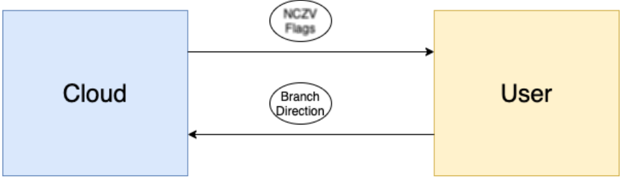
### Visual Description
## Diagram: Cloud-User Interaction
### Overview
The image is a simple diagram illustrating the interaction between a "Cloud" and a "User". It shows a two-way communication flow, with "NCZV Flags" being sent from the Cloud to the User, and a "Branch Direction" being sent from the User to the Cloud.
### Components/Axes
* **Cloud:** A light blue rectangle on the left side of the diagram, labeled "Cloud".
* **User:** A light yellow rectangle on the right side of the diagram, labeled "User".
* **NCZV Flags:** An oval shape above the horizontal center of the diagram, labeled "NCZV Flags". An arrow points from the Cloud to the User, indicating the direction of the flags.
* **Branch Direction:** An oval shape below the horizontal center of the diagram, labeled "Branch Direction". An arrow points from the User to the Cloud, indicating the direction of the branch.
### Detailed Analysis
* **Cloud:** The "Cloud" rectangle is positioned on the left side of the diagram.
* **User:** The "User" rectangle is positioned on the right side of the diagram.
* **NCZV Flags:** The arrow associated with "NCZV Flags" originates from the right side of the "Cloud" rectangle and terminates at the left side of the "User" rectangle.
* **Branch Direction:** The arrow associated with "Branch Direction" originates from the right side of the "User" rectangle and terminates at the left side of the "Cloud" rectangle.
### Key Observations
* The diagram illustrates a two-way communication between the Cloud and the User.
* "NCZV Flags" are sent from the Cloud to the User.
* "Branch Direction" is sent from the User to the Cloud.
### Interpretation
The diagram represents a simplified model of interaction between a cloud service and a user. The "NCZV Flags" likely represent some form of data or control signals being sent from the cloud to the user. The "Branch Direction" likely represents a user's request or instruction being sent back to the cloud, potentially influencing the cloud's behavior or data processing. The diagram highlights the bidirectional nature of the interaction, where both the cloud and the user can initiate communication.
</details>
## VII. RESULTS
This section reports on ( i ) the scalability with respect to bit count when the core count is a fixed number; ( ii ) the scalability with respect to core count when the data size is a fixed number; ( iii ) on CryptoEmu's potential vulnerabilities; and ( iv ) comparison against the state of the art.
## A. Scalability with respect to bit count
Table I shows the latency of the TFHE library API. Non-bootstrapped gates such as CONSTANT, NOT, and COPY are three to four orders of magnitude faster than bootstrapped gates. Therefore, compared to bootstrapped gates, non-bootstrapped
gates are considered as negligible in the CryptoEmu's performance equation. Functional units without bootstrapped gates are not included in our scalability analysis.
The latency of a single bootstrapped gate is denoted as G . In the rest of the subsection, we analyzed the scalability of functional unit subroutines with respect to data size N. Two scenarios are considered: single core mode, and multi-core mode with a sufficient number of cores to do all intended parallel computation concurrently. CryptoEmu uses all available cores to concurrently perform homomorphic computation on encrypted data with multi-core mode latency. When CryptoEmu exhausted all core resources, the rest of the program will be serialized with single-core mode latency.
a) Adder.: An adder has 3 stages: Generate and propagate calculation, carry calculation, and sum calculation. Let the available core number be 1 (single core mode); then, the time complexity for each stage is:
Generate and propagate calculation : To compute generate and propagate for one bit, two bootstrapped FHE gates evaluations are required. With N-bit operands, total latency is 2 · G · N .
Carry calculation : Three bootstrapped FHE gates evaluations are required to calculate the carry out bit. With N-bit operands, total latency is 3 · G · N .
Sum calculation : One bootstrapped XOR gate is needed to calculate one sum bit. With N-bit operands, total latency is G · N Total latency : The latency for adder with single core is 6 · G · N . Time complexity is O ( N ) .
Table XVI summarizes the discussion above for the N-bit adder with one core available.
TABLE XVI: Adder scalability, single core
| Operation | Latency | Time complexity |
|-------------------|-----------|-------------------|
| (g,p) calculation | 2 GN | O ( N ) |
| Carry calculation | 3 GN | O ( N ) |
| Sum calculation | GN | O ( N ) |
| Total latency | 6 GN | O ( N ) |
Assume a sufficient but fixed number of processors are available. Then, the latencies become:
Generate and propagate : Calculation for generate and propagate for one bit can be executed in parallel, with a latency of one bootstrapped FHE gate. Given N-bit operands, N calculations can be carried out concurrently. Therefore, the latency for the (g,p) calculation is G .
Carry calculation : Carry out computation for one bit can be executed in parallel, with a latency of two bootstrapped FHE gates. For N-bit operands, carry calculation is divided into log ( N ) stages. Operations in the same stage are executed in parallel. Therefore, latency for carry calculation is 2 · G · log ( N ) .
Sum calculation : Each sum bit needs one bootstrapped XOR gate. For N-bit operands, N computations can be executed in parallel. Total latency for sum calculation is G .
Total latency : The total latency for an adder with sufficient yet fixed number of cores is 2 · G · log ( N )+2 G . Time complexity is O ( log ( N )) .
Table XVII summarizes the scalability analysis discussion for the N-bit adder with sufficient, yet fixed number of cores available.
TABLE XVII: Adder scalability, multiple core
| Operation | Latency | Time complexity |
|-------------------|---------------------|-------------------|
| (g,p) calculation | G | O (1) |
| Carry calculation | 2 G · log ( N ) | O ( log ( N )) |
| Sum calculation | G | O (1) |
| Total latency | 2 G · log ( N )+2 G | O ( log ( N )) |
b) Subtractor.: A subtractor performs homomorphic negation on subtrahend, and homomorphically adds subtrahend's complement to minuend using an adder with carry in of one.
Negation uses TFHE library's non-bootstrapped NOT gate, and its latency is negligible. Adding a carry to the adder uses two extra bootstrapped gates. Therefore, the total latency for subtractor is Latency ( Adder ) + 2 · G .
Table XVIII summarizes key scalability aspects for the N-bit subtractor with single core and with sufficient yet fixed number of cores available.
TABLE XVIII: Subtractor scalability
| # of cores | Latency | Time complexity |
|--------------|------------------|-------------------|
| Single core | 6 GN +2 G | O ( N ) |
| Multi-core | 2 Glog ( N )+4 G | O ( log ( N )) |
Shifter. For shifting with cleartext immediate, the operation is essentially a homomorphic data movement operation using the TFHE library's COPY and CONSTANT API. Shifting with immediate latency is therefore negligible compared to the rest of function units in CryptoEmu.
.
Shifting with encrypted vReg is implemented as a barrel shifter. For vReg N-bit shift, the operation has log ( N ) stages. In each stage, individual bits are selected by bits in the shifting amount vReg moves to the next stage through a MUX. The TFHE MUX has latency around 2 · G .
When a single core is used, each stage has N MUXs. Latency in one stage is 2 · G · N . There are log ( N ) stages, therefore total shifter latency for a single core processor is 2 · G · N · log ( N ) .
When sufficient cores are given, MUXs of the same stage can be evaluated in parallel, resulting in a latency of 2 · G . There are log ( N ) stages, therefore total shifter latency for processor with sufficient cores is 2 · G · log ( N ) .
Table XIX summarizes key scalability aspects for the shifter with respect to bit count N, in single core and multi-core mode.
TABLE XIX: Shifter scalability
| # of cores | Latency | Time complexity |
|--------------|---------------|-------------------|
| Single core | 2 GNlog ( N ) | O ( Nlog ( N )) |
| Multi-core | 2 Glog ( N ) | O ( log ( N )) |
c) Multiplier.: The multiplier is implemented with iterative multiplication algorithms. A multiplier with N-bit operands requires N times iterations.
N-bit unsigned multiplication contains an N-bit FHE AND evaluation and invokes an N-bit adder for every iteration. When running unsigned multiplication with a single core, sequential latency for N-bit FHE AND is N · G . Sequential latency for the N-bit adder is 6 · G · N . Latency for one iteration is 7 · G · N . Total latency for the N-bit unsigned multiplication 7 · G · N 2 .
When sufficient number of cores are provided to run subroutines in parallel, parallel latency for the N-bit FHE AND is G . Parallel latency for N-bit adder is 2 · G · log ( N ) + 2 G . One iteration takes 2 · G · log ( N ) + 3 G to complete. Total latency for N-bit unsigned multiplication is 2 · G · N · log ( N ) + 3 · G · N .
Signed multiplication has the same latency per iteration as in unsigned multiplication. N-bit signed multiplication involves an N-bit addition that adds an offset to the upper half of the 2N-bit product. This operation has sequential latency of 6 · G · N and parallel latency of 2 · G · log ( N ) + 3 G . Total latency for signed multiplication is therefore 7 · G · N 2 +6 · G · N for single core, and 2 · G · N · log ( N ) + 3 · G · N +2 · G · log ( N ) + 3 G if a sufficient number of cores is available.
Table XX summarizes key scalability aspects (latency and time complexity) for the unsigned and signed multiplication with respect to bit count N, in single core and multi-core mode.
TABLE XX: Multiplier scalability
| unsigned? | # of cores | Latency | Time complexity |
|-------------|--------------|--------------------------------------|-------------------|
| Yes | Single core | 7 GN 2 | O ( N 2 )) |
| Yes | Multi-core | 2 GNlog ( N )+3 GN | O ( Nlog ( N )) |
| No | Single core | 7 GN 2 +6 GN | O ( N 2 )) |
| No | Multi-core | 2 GNlog ( N )+3 GN +2 Glog ( N )+3 G | O ( Nlog ( N )) |
d) Divider.: The divider is implemented with iterative non-restoring division algorithm. A divider with N-bit operands requires N iterations. Every iteration involves negligible non-bootstrapped gates and an adder-subtractor unit. The addersubtractor selectively inverts the second operand based on the value in the SUB bit. Then the subroutine invokes an adder to add the first operand, processes the second operand, and SUB bit together to form a result.
For computation on single core, selective inversion for an N-bit operand uses N FHE XOR gates, and therefore has a latency of G · N . Adder with carry in has 6 · G · N +2 · G latency. Latency per iteration is 7 · G · N +2 · G , and total latency is 7 · G · N 2 +2 · G · N for single core.
If enough cores are available, the N-bit selective inversion can be executed in parallel, resulting in G latency. Adder with carry in parallel computing mode has 2 · G · log ( N ) + 4 · G latency. Latency per iteration is 2 · G · log ( N ) + 5 · G , and total latency is 2 · G · N · log ( N ) + 5 · G · N .
Table XXI shows latency and time complexity results for the unsigned division with respect to bit count N, in single core and multi-core modes.
TABLE XXI: Divider scalability
| # of cores | Latency | Time complexity |
|--------------|--------------------|-------------------|
| Single core | 7 GN 2 +2 GN | O ( N 2 )) |
| Multi-core | 2 GNlog ( N )+5 GN | O ( Nlog ( N )) |
e) Bitwise operations.: Bitwise operation evaluates all input bits with one FHE gate. Latency per bit is G . For N-bit bitwise operation in single core mode, total latency is G · N . In multi-core mode, because all FHE gate evaluations are in parallel, the total latency is G .
Table XXI shows latency and time complexity data for bitwise operation with respect to bit count N, in single core and multi-core mode.
TABLE XXII: Bitwise ops scalability
| # of cores | Latency | Time complexity |
|--------------|-----------|-------------------|
| Single core | GN | O ( N ) |
| Multi-core | G | O (1) |
f) Conditional Flags.: Conditional flags calculation involves four sub-calculations: N flag, Z flag, C flag, and V flag. N flag and C flag calculations are trivial. Z flag calculation contains an OR reduction operation. In single core mode, the N-bit Z flag calculation has a latency of G · N . In multi-core mode, the OR reduction is executed in parallel. N-bit OR reduction is broken down into log ( N ) stages, and in each stage, the FHE OR gates are evaluated in parallel. The N-bit Z flag latency for parallel computing is Glog ( N ) .
The V flag calculation uses five gates regardless of the size of the input vReg. In single core mode, V flag calculation has 5 · G latency. In multi-core mode because V flag calculation can be partially optimized with parallel computing, the latency is 3 · G . Therefore, total latency for single core mode is G · N +5 · G , and total latency for multi-core mode is G · log ( N ) +3 · G .
Table XXIII shows latency and time complexity data for conditional flag calculation with respect to the bit count N, in single core and multi-core mode.
TABLE XXIII: Conditional flags scalability
| # of cores | Latency | Time complexity |
|--------------|----------------|-------------------|
| Single core | GN +5 G | O ( N ) |
| Multi-core | Glog ( N )+3 G | O ( log ( N )) |
## B. Scalability with respect to core count
CryptoEmu's performance is dictated by the extent to which it can rely on parallel computing. In ideal scenario, the processor has enough cores to enable any collection of tasks that can be performed in parallel to be processed as such. Sometimes, a part of the execution of an instruction takes place in parallel, but the rest is sequential because all CPU core resources are exhausted. In the worst case scenario, the processor has only one core and all computations are sequential/serialized.
Assume that the size of the functional units is 16-bit. Peak thread usage is then 32 threads, where each thread performance an FHE gate evaluation. On the server used in this study, which has 48 cores distributed over four CPUs, we vary the number of cores available to carry our emulation from 1 core to 48 cores. This amounts to a strong scaling analysis. We created scenarios where ( i ) the instruction set can draw on one core only and therefore the computation is sequential; ( ii ) the instruction set has insufficient cores and parallel computation is mixed with sequential computation; and ( iii ) the instruction set can count on sufficient cores to do all emulation in parallel.
a) Adder.: Figure 18 shows the 16-bit adder's compute time with respect to core count. From the chart, the adder's latency decreases when the core count increases from 1 to 32. The adder reached its optimal speed at around 32 core count and has a slight decrease in speed when the core count exceeds 32. Adder's maximum speedup from parallel computing is around 7.78x.
Fig. 18: Time vs Core count
<details>
<summary>Image 20 Details</summary>
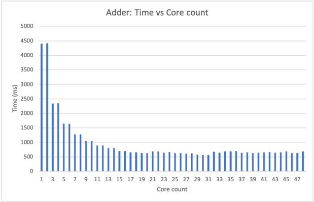
### Visual Description
## Bar Chart: Adder: Time vs Core count
### Overview
The image is a bar chart titled "Adder: Time vs Core count". It illustrates the relationship between the number of cores used and the time taken for an adder operation. The x-axis represents the core count, ranging from 1 to 47. The y-axis represents the time in milliseconds (ms), ranging from 0 to 5000. The chart shows a general trend of decreasing time with an increasing number of cores, up to a certain point, after which the time plateaus.
### Components/Axes
* **Title:** Adder: Time vs Core count
* **X-axis:**
* Label: Core count
* Scale: 1, 3, 5, 7, 9, 11, 13, 15, 17, 19, 21, 23, 25, 27, 29, 31, 33, 35, 37, 39, 41, 43, 45, 47
* **Y-axis:**
* Label: Time (ms)
* Scale: 0, 500, 1000, 1500, 2000, 2500, 3000, 3500, 4000, 4500, 5000
* **Data Series:**
* The chart contains a single data series represented by blue bars.
### Detailed Analysis
The data series shows the time taken for the adder operation for different core counts.
* **Core Count 1:** Time is approximately 4400 ms.
* **Core Count 3:** Time is approximately 2300 ms.
* **Core Count 5:** Time is approximately 1650 ms.
* **Core Count 7:** Time is approximately 1400 ms.
* **Core Count 9:** Time is approximately 1100 ms.
* **Core Count 11:** Time is approximately 1000 ms.
* **Core Count 13:** Time is approximately 850 ms.
* **Core Count 15:** Time is approximately 750 ms.
* **Core Count 17:** Time is approximately 700 ms.
* **Core Count 19:** Time is approximately 650 ms.
* **Core Count 21:** Time is approximately 650 ms.
* **Core Count 23:** Time is approximately 600 ms.
* **Core Count 25:** Time is approximately 600 ms.
* **Core Count 27:** Time is approximately 600 ms.
* **Core Count 29:** Time is approximately 550 ms.
* **Core Count 31:** Time is approximately 600 ms.
* **Core Count 33:** Time is approximately 650 ms.
* **Core Count 35:** Time is approximately 650 ms.
* **Core Count 37:** Time is approximately 650 ms.
* **Core Count 39:** Time is approximately 650 ms.
* **Core Count 41:** Time is approximately 650 ms.
* **Core Count 43:** Time is approximately 650 ms.
* **Core Count 45:** Time is approximately 650 ms.
* **Core Count 47:** Time is approximately 650 ms.
The time decreases rapidly from 1 core to around 11 cores. After 11 cores, the decrease in time becomes much smaller, and the time plateaus around 600-700 ms.
### Key Observations
* The time taken for the adder operation decreases significantly as the number of cores increases from 1 to approximately 11.
* Beyond 11 cores, the benefit of adding more cores diminishes, and the time plateaus.
* There is a significant drop in time from 1 core to 3 cores.
### Interpretation
The chart demonstrates the performance improvement achieved by parallelizing the adder operation using multiple cores. The initial rapid decrease in time indicates that the operation benefits significantly from parallel processing. However, the plateauing of the time beyond a certain number of cores suggests that there are diminishing returns to adding more cores. This could be due to factors such as communication overhead between cores, limitations in the algorithm's parallelizability, or hardware constraints. The optimal number of cores for this adder operation appears to be around 11, as adding more cores beyond this point does not significantly reduce the execution time.
</details>
b) Subtractor.: Figure 19 shows the 16-bit subtractor's compute time with respect to core count. The 16-bit subtractor uses at most 32 cores to compute in parallel. The subtractor's latency decreases as the core count increases from 1-32, and reaches its maximum performance at around 32 core count. At and beyond 32 core count, all parallel optimizations are enabled. When the core counts saturate the subtractor's parallel computing requirement, the latency of the subtractor is around 700ms. The subtractor's maximum speedup from parallel computing is about 8.49x.
Fig. 19: Time vs Core count
<details>
<summary>Image 21 Details</summary>
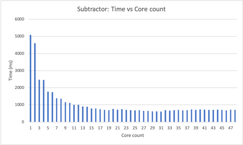
### Visual Description
## Bar Chart: Subtractor: Time vs Core count
### Overview
The image is a bar chart that displays the relationship between the time taken (in milliseconds) and the core count for a "Subtractor" operation. The x-axis represents the core count, ranging from 1 to 47. The y-axis represents the time in milliseconds, ranging from 0 to 6000. The chart shows a general trend of decreasing time with an increasing number of cores, with a steep drop initially, followed by a more gradual decrease.
### Components/Axes
* **Title:** Subtractor: Time vs Core count
* **X-axis:**
* Label: Core count
* Scale: 1 to 47, incrementing by 2 (1, 3, 5, 7, ..., 47)
* **Y-axis:**
* Label: Time (ms)
* Scale: 0 to 6000, incrementing by 1000 (0, 1000, 2000, 3000, 4000, 5000, 6000)
* **Data:** Blue bars representing the time taken for each core count.
### Detailed Analysis
Here's a breakdown of the approximate time values for different core counts:
* **1 Core:** Approximately 5050 ms
* **3 Cores:** Approximately 4600 ms
* **5 Cores:** Approximately 2450 ms
* **7 Cores:** Approximately 1750 ms
* **9 Cores:** Approximately 1700 ms
* **11 Cores:** Approximately 1350 ms
* **13 Cores:** Approximately 1000 ms
* **15 Cores:** Approximately 950 ms
* **17 Cores:** Approximately 800 ms
* **19 Cores:** Approximately 750 ms
* **21 Cores:** Approximately 700 ms
* **23 Cores:** Approximately 700 ms
* **25 Cores:** Approximately 650 ms
* **27 Cores:** Approximately 650 ms
* **29 Cores:** Approximately 600 ms
* **31 Cores:** Approximately 600 ms
* **33 Cores:** Approximately 650 ms
* **35 Cores:** Approximately 650 ms
* **37 Cores:** Approximately 650 ms
* **39 Cores:** Approximately 650 ms
* **41 Cores:** Approximately 700 ms
* **43 Cores:** Approximately 700 ms
* **45 Cores:** Approximately 700 ms
* **47 Cores:** Approximately 700 ms
**Trend:** The time decreases rapidly from 1 core to approximately 11 cores. After that, the decrease is much slower, and the time seems to plateau around 700 ms.
### Key Observations
* The most significant reduction in time occurs when increasing the core count from 1 to around 11.
* Beyond 11 cores, the benefit of adding more cores diminishes significantly.
* The time appears to stabilize around 700 ms for core counts greater than 35.
### Interpretation
The data suggests that increasing the number of cores for the "Subtractor" operation initially leads to a substantial reduction in processing time, indicating effective parallelization. However, after a certain point (around 11 cores), the gains from adding more cores become marginal. This could be due to factors such as communication overhead between cores, limitations in the algorithm's parallelizability, or other bottlenecks in the system. The plateauing of time around 700 ms suggests that there might be a fundamental limit to how fast the operation can be performed, regardless of the number of cores used.
</details>
c) Shifter.: Figure 20 shows the 16-bit shifter's compute time with respect to core count. A 16-bit shifter has a maximum core usage of 16. The 16-bit shifter's latency decreases as the core count increases from 1-16. The shifter's performance reaches its peak at core count 16. For core counts higher than 16, its stays stable at around 300ms. The maximum speedup yielded by parallel computing is around 10.94x.
Fig. 20: Time vs Core count
<details>
<summary>Image 22 Details</summary>
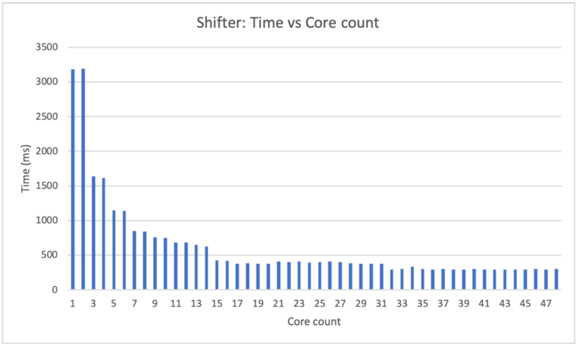
### Visual Description
## Bar Chart: Shifter - Time vs Core Count
### Overview
The image is a bar chart titled "Shifter: Time vs Core count". It shows the relationship between the number of cores used and the time taken (in milliseconds). The x-axis represents the core count, ranging from 1 to 47. The y-axis represents the time in milliseconds, ranging from 0 to 3500. The chart displays a trend where the time taken decreases as the core count increases, eventually leveling off.
### Components/Axes
* **Title:** Shifter: Time vs Core count
* **X-axis:**
* Label: Core count
* Scale: 1, 3, 5, 7, 9, 11, 13, 15, 17, 19, 21, 23, 25, 27, 29, 31, 33, 35, 37, 39, 41, 43, 45, 47
* **Y-axis:**
* Label: Time (ms)
* Scale: 0, 500, 1000, 1500, 2000, 2500, 3000, 3500
* **Data Series:** The chart contains one data series represented by blue bars.
### Detailed Analysis
The data series shows a decreasing trend in time (ms) as the core count increases.
* **Core Count 1:** Time is approximately 3200 ms.
* **Core Count 3:** Time is approximately 1600 ms.
* **Core Count 5:** Time is approximately 1600 ms.
* **Core Count 7:** Time is approximately 1100 ms.
* **Core Count 9:** Time is approximately 800 ms.
* **Core Count 11:** Time is approximately 750 ms.
* **Core Count 13:** Time is approximately 650 ms.
* **Core Count 15:** Time is approximately 500 ms.
* **Core Count 17:** Time is approximately 400 ms.
* **Core Count 19:** Time is approximately 400 ms.
* **Core Count 21:** Time is approximately 400 ms.
* **Core Count 23:** Time is approximately 400 ms.
* **Core Count 25:** Time is approximately 350 ms.
* **Core Count 27:** Time is approximately 350 ms.
* **Core Count 29:** Time is approximately 350 ms.
* **Core Count 31:** Time is approximately 350 ms.
* **Core Count 33:** Time is approximately 300 ms.
* **Core Count 35:** Time is approximately 300 ms.
* **Core Count 37:** Time is approximately 300 ms.
* **Core Count 39:** Time is approximately 300 ms.
* **Core Count 41:** Time is approximately 300 ms.
* **Core Count 43:** Time is approximately 300 ms.
* **Core Count 45:** Time is approximately 300 ms.
* **Core Count 47:** Time is approximately 300 ms.
### Key Observations
* The most significant drop in time occurs between 1 and 3 cores.
* After approximately 31 cores, the time taken plateaus around 300 ms.
* There is a diminishing return in time reduction as the core count increases beyond a certain point.
### Interpretation
The chart demonstrates the impact of increasing core count on the execution time of the "Shifter" process. Initially, adding more cores significantly reduces the execution time. However, as the core count increases, the reduction in time becomes less pronounced, indicating a point of diminishing returns. This suggests that there is an optimal core count beyond which adding more cores does not significantly improve performance, possibly due to overhead or other limiting factors. The data implies that for this specific "Shifter" process, using more than 31 cores provides minimal benefit in terms of reducing execution time.
</details>
d) Multiplier.: Figure 21 shows the 16-bit multiplier's compute time with respect to core count. A 16-bit multiplier requires 32 cores to enable all parallel computing optimization. From the chart, both unsigned and signed multiplication's latency decrease as the number of cores increases from 1 to 32. The multiplier reached its top speed at around 32 cores. Beyond that, the multiplier's latency stays around 11000-12000ms. Unsigned multiplication has a maximum parallel computing speedup of 8.3x; signed multiplication has a maximum parallel computing speedup of 8.4x.
Fig. 21: Time vs Core count
<details>
<summary>Image 23 Details</summary>
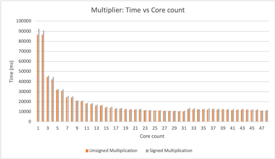
### Visual Description
## Bar Chart: Multiplier: Time vs Core count
### Overview
The image is a bar chart comparing the execution time (in milliseconds) of unsigned and signed multiplication operations against the number of cores used (Core count). The chart displays two data series: "Unsigned Multiplication" (orange bars) and "Signed Multiplication" (gray bars). The x-axis represents the core count, ranging from 1 to 47. The y-axis represents the time in milliseconds, ranging from 0 to 100,000.
### Components/Axes
* **Title:** Multiplier: Time vs Core count
* **X-axis:**
* Label: Core count
* Scale: 1, 3, 5, 7, 9, 11, 13, 15, 17, 19, 21, 23, 25, 27, 29, 31, 33, 35, 37, 39, 41, 43, 45, 47
* **Y-axis:**
* Label: Time (ms)
* Scale: 0, 10000, 20000, 30000, 40000, 50000, 60000, 70000, 80000, 90000, 100000
* **Legend:** Located at the bottom of the chart.
* Unsigned Multiplication: Orange bars
* Signed Multiplication: Gray bars
### Detailed Analysis
**Unsigned Multiplication (Orange Bars):**
* **Trend:** The execution time decreases rapidly from 1 core to approximately 11 cores, then gradually decreases until around 31 cores, after which it stabilizes.
* **Data Points:**
* 1 core: ~86000 ms
* 3 cores: ~45000 ms
* 5 cores: ~32000 ms
* 7 cores: ~26000 ms
* 9 cores: ~22000 ms
* 11 cores: ~19000 ms
* 13 cores: ~17000 ms
* 15 cores: ~15000 ms
* 17 cores: ~14000 ms
* 19 cores: ~13000 ms
* 21 cores: ~12000 ms
* 23 cores: ~12000 ms
* 25 cores: ~11000 ms
* 27 cores: ~11000 ms
* 29 cores: ~11000 ms
* 31 cores: ~11000 ms
* 33 cores: ~12000 ms
* 35 cores: ~12000 ms
* 37 cores: ~12000 ms
* 39 cores: ~12000 ms
* 41 cores: ~12000 ms
* 43 cores: ~12000 ms
* 45 cores: ~12000 ms
* 47 cores: ~11000 ms
**Signed Multiplication (Gray Bars):**
* **Trend:** The execution time decreases rapidly from 1 core to approximately 11 cores, then gradually decreases until around 31 cores, after which it stabilizes. The signed multiplication times are consistently slightly higher than the unsigned multiplication times.
* **Data Points:**
* 1 core: ~92000 ms
* 3 cores: ~48000 ms
* 5 cores: ~34000 ms
* 7 cores: ~27000 ms
* 9 cores: ~23000 ms
* 11 cores: ~20000 ms
* 13 cores: ~18000 ms
* 15 cores: ~16000 ms
* 17 cores: ~15000 ms
* 19 cores: ~14000 ms
* 21 cores: ~13000 ms
* 23 cores: ~12000 ms
* 25 cores: ~12000 ms
* 27 cores: ~12000 ms
* 29 cores: ~12000 ms
* 31 cores: ~12000 ms
* 33 cores: ~13000 ms
* 35 cores: ~13000 ms
* 37 cores: ~13000 ms
* 39 cores: ~13000 ms
* 41 cores: ~13000 ms
* 43 cores: ~13000 ms
* 45 cores: ~13000 ms
* 47 cores: ~12000 ms
### Key Observations
* Both unsigned and signed multiplication times decrease significantly as the core count increases from 1 to approximately 11.
* After 11 cores, the decrease in execution time becomes more gradual.
* The execution time stabilizes around 31 cores, with minimal improvement beyond that point.
* Signed multiplication consistently takes slightly longer than unsigned multiplication for the same core count.
### Interpretation
The data suggests that increasing the number of cores significantly reduces the execution time for both unsigned and signed multiplication operations, up to a certain point. The diminishing returns observed after approximately 11 cores indicate that there is a limit to the benefits of adding more cores for this specific task. The slight difference in execution time between signed and unsigned multiplication likely reflects the additional overhead involved in handling signed numbers. The stabilization of execution time after 31 cores suggests that the task becomes limited by other factors, such as memory bandwidth or inter-process communication overhead, rather than the number of available cores.
</details>
e) Divider.: Figure 22 shows the 16-bit divider's compute time with respect to core count. A 16-bit divider requires 32 cores to achieve the best parallel computing performance. From the chart, divider's latency decreases as the core count increases from 1 to 32. From 32 cores on, the divider's latency stays at around 12000ms. The 16-bit divider has a maximum parallel computing speedup of 8.43x, reached when it can draw on 32 cores.
Fig. 22: Time vs Core count
<details>
<summary>Image 24 Details</summary>
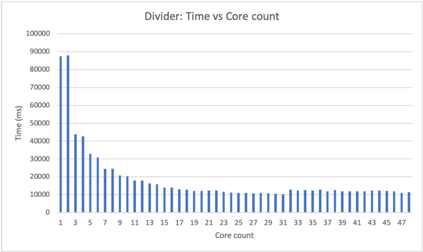
### Visual Description
## Bar Chart: Divider: Time vs Core count
### Overview
The image is a bar chart that displays the relationship between the execution time (in milliseconds) and the number of cores used. The chart title is "Divider: Time vs Core count". The x-axis represents the core count, ranging from 1 to 47. The y-axis represents the time in milliseconds, ranging from 0 to 100,000. The chart shows a general trend of decreasing execution time as the core count increases, with the most significant drop occurring between 1 and approximately 15 cores. After 15 cores, the execution time plateaus.
### Components/Axes
* **Title:** Divider: Time vs Core count
* **X-axis:**
* Label: Core count
* Scale: 1, 3, 5, 7, 9, 11, 13, 15, 17, 19, 21, 23, 25, 27, 29, 31, 33, 35, 37, 39, 41, 43, 45, 47
* **Y-axis:**
* Label: Time (ms)
* Scale: 0, 10000, 20000, 30000, 40000, 50000, 60000, 70000, 80000, 90000, 100000
### Detailed Analysis
The chart presents data for the execution time with varying core counts. The data is represented by blue bars.
* **Core Count 1:** Time is approximately 87000 ms.
* **Core Count 3:** Time is approximately 87000 ms.
* **Core Count 5:** Time is approximately 43000 ms.
* **Core Count 7:** Time is approximately 32000 ms.
* **Core Count 9:** Time is approximately 30000 ms.
* **Core Count 11:** Time is approximately 24000 ms.
* **Core Count 13:** Time is approximately 21000 ms.
* **Core Count 15:** Time is approximately 18000 ms.
* **Core Count 17:** Time is approximately 16000 ms.
* **Core Count 19:** Time is approximately 14000 ms.
* **Core Count 21:** Time is approximately 13000 ms.
* **Core Count 23:** Time is approximately 12000 ms.
* **Core Count 25:** Time is approximately 11000 ms.
* **Core Count 27:** Time is approximately 11000 ms.
* **Core Count 29:** Time is approximately 11000 ms.
* **Core Count 31:** Time is approximately 11000 ms.
* **Core Count 33:** Time is approximately 12000 ms.
* **Core Count 35:** Time is approximately 11000 ms.
* **Core Count 37:** Time is approximately 11000 ms.
* **Core Count 39:** Time is approximately 11000 ms.
* **Core Count 41:** Time is approximately 11000 ms.
* **Core Count 43:** Time is approximately 11000 ms.
* **Core Count 45:** Time is approximately 11000 ms.
* **Core Count 47:** Time is approximately 11000 ms.
### Key Observations
* The execution time decreases rapidly as the core count increases from 1 to approximately 15.
* After 15 cores, the execution time plateaus and remains relatively constant.
* The most significant reduction in execution time occurs when moving from 1 core to 5 cores.
### Interpretation
The data suggests that increasing the number of cores initially leads to a significant reduction in execution time. This indicates that the "Divider" task can be parallelized and benefit from using multiple cores. However, after a certain point (around 15 cores), adding more cores does not result in a substantial decrease in execution time. This could be due to factors such as communication overhead between cores, limitations in the algorithm's parallelizability, or resource contention. The chart demonstrates diminishing returns with increasing core count, suggesting an optimal number of cores for this specific task lies somewhere around 15.
</details>
f) Bitwise operations.: Figure 23 shows 16-bit bitwise operation's compute time with respect to the core count. 16-bit bitwise ops requires 16 cores to have the best parallel computing performance. From the graph, at core count 16 the bitwise operation reached its top speed. At 16 cores and beyond, the latency stays around 50ms. 16-bit bitwise op has a maximum parallel computing speedup of 8.63x.
Fig. 23: Time vs Core count
<details>
<summary>Image 25 Details</summary>
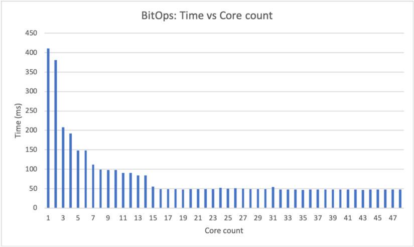
### Visual Description
## Bar Chart: BitOps: Time vs Core count
### Overview
The image is a bar chart titled "BitOps: Time vs Core count". The chart displays the relationship between the number of cores (x-axis) and the time in milliseconds (y-axis). The data shows a decreasing trend in time as the core count increases, particularly at lower core counts, with the time stabilizing around 50ms for higher core counts.
### Components/Axes
* **Title:** BitOps: Time vs Core count
* **X-axis:** Core count, with integer values from 1 to 47, incrementing by 2.
* **Y-axis:** Time (ms), with values ranging from 0 to 450, incrementing by 50.
* **Data Series:** Single data series represented by blue bars.
### Detailed Analysis
The chart presents a single data series, represented by blue bars, showing the time (in milliseconds) for different core counts.
Here are approximate values for some core counts:
* **Core count 1:** Approximately 400 ms
* **Core count 3:** Approximately 210 ms
* **Core count 5:** Approximately 150 ms
* **Core count 7:** Approximately 110 ms
* **Core count 9:** Approximately 100 ms
* **Core count 11:** Approximately 95 ms
* **Core count 13:** Approximately 90 ms
* **Core count 15:** Approximately 85 ms
* **Core count 17 to 47:** Approximately 50 ms
The trend shows a rapid decrease in time from 1 core to approximately 15 cores. After 15 cores, the time stabilizes around 50 ms.
### Key Observations
* The time decreases significantly as the core count increases from 1 to 15.
* Beyond 15 cores, the time remains relatively constant at approximately 50 ms.
* There is a diminishing return in performance gain as the core count increases beyond 15.
### Interpretation
The data suggests that increasing the core count initially leads to a significant reduction in processing time. However, after a certain point (around 15 cores in this case), adding more cores does not result in a substantial improvement in performance. This could be due to factors such as Amdahl's Law, where the sequential portion of the task limits the benefits of parallelization, or overhead associated with managing a large number of cores. The chart demonstrates the concept of diminishing returns in parallel computing, where the performance gains from adding more processors decrease as the number of processors increases.
</details>
- g) Conditional Flags.: Figure 24 shows the 16-bit conditional flag unit's compute time with respect to core count. A 16-bit conditional flag unit runs a maximum of 18 threads in parallel. On the chart from core count 15 onward, the latency of the conditional flag unit hovers at around 120-130ms. The maximum parallel computing speedup is 4.7x.
Fig. 24: Time vs Core count
<details>
<summary>Image 26 Details</summary>
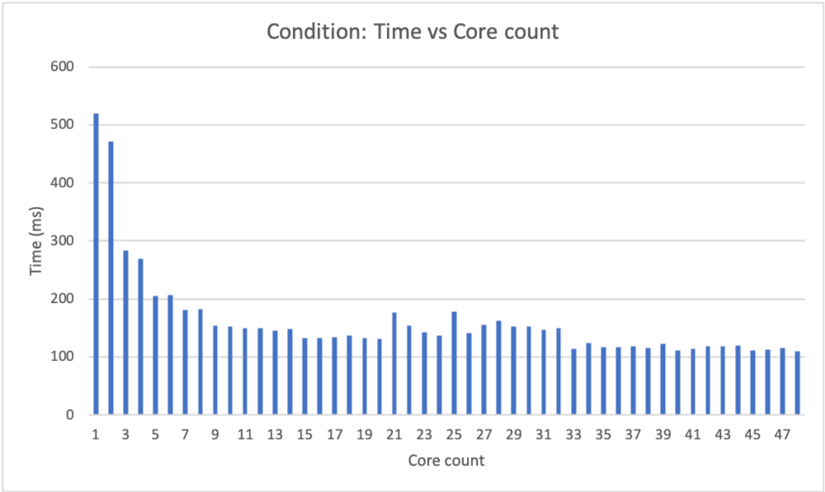
### Visual Description
## Bar Chart: Condition: Time vs Core count
### Overview
The image is a bar chart that displays the relationship between "Time (ms)" and "Core count". The chart shows how the time taken (in milliseconds) varies with the number of cores used. The bars are blue.
### Components/Axes
* **Title:** Condition: Time vs Core count
* **X-axis:** Core count, labeled from 1 to 47 in increments of 2.
* **Y-axis:** Time (ms), labeled from 0 to 600 in increments of 100.
### Detailed Analysis
The chart presents data for core counts from 1 to 47. The time values for each core count are represented by the height of the blue bars.
* **Core Count 1:** Time is approximately 520 ms.
* **Core Count 3:** Time is approximately 470 ms.
* **Core Count 5:** Time is approximately 280 ms.
* **Core Count 7:** Time is approximately 200 ms.
* **Core Count 9:** Time is approximately 180 ms.
* **Core Count 11:** Time is approximately 150 ms.
* **Core Count 13:** Time is approximately 130 ms.
* **Core Count 15:** Time is approximately 130 ms.
* **Core Count 17:** Time is approximately 130 ms.
* **Core Count 19:** Time is approximately 130 ms.
* **Core Count 21:** Time is approximately 140 ms.
* **Core Count 23:** Time is approximately 180 ms.
* **Core Count 25:** Time is approximately 140 ms.
* **Core Count 27:** Time is approximately 160 ms.
* **Core Count 29:** Time is approximately 150 ms.
* **Core Count 31:** Time is approximately 150 ms.
* **Core Count 33:** Time is approximately 120 ms.
* **Core Count 35:** Time is approximately 120 ms.
* **Core Count 37:** Time is approximately 120 ms.
* **Core Count 39:** Time is approximately 120 ms.
* **Core Count 41:** Time is approximately 120 ms.
* **Core Count 43:** Time is approximately 120 ms.
* **Core Count 45:** Time is approximately 120 ms.
* **Core Count 47:** Time is approximately 110 ms.
The trend shows a rapid decrease in time as the core count increases from 1 to approximately 11. After that, the time values fluctuate between approximately 110 ms and 180 ms, with no clear trend.
### Key Observations
* The time taken is significantly higher for lower core counts (1-5).
* The time decreases sharply as the core count increases initially.
* Beyond a core count of approximately 11, the time stabilizes and fluctuates within a narrow range.
### Interpretation
The data suggests that increasing the core count initially leads to a significant reduction in processing time. However, after a certain point (around 11 cores), adding more cores does not result in a substantial decrease in time. This could indicate that the task being measured has a limit to how much it can be parallelized, or that other factors become the bottleneck beyond a certain number of cores. The initial drop indicates that parallel processing is effective up to a point, but diminishing returns are observed as the core count increases further.
</details>
## C. Vulnerability
There are two source of vulnerability associated with the current CryptoEmu implementation: ( i ) the unencrypted HE instruction memory; and ( ii ) the branch resolution process.
Because HE instruction memory is in cleartext, the cloud knows exactly what assembly code is being executed. Assumption 2 assumes that the cloud is honest, so cloud visible instructions to the cloud do not pose a security issue. However, it is possible that the cloud's execution pipeline is compromised by attackers. If an attacker obtains control over the instruction set emulator, or performs a side-channel attack, user data can be breached.
If Assumption 2 is lifted, then the unencrypted HE instruction memory becomes a security loophole.Note that, we still assume the cloud will not start a denial of service attack on user. For example, if user send an encrypted number such as age, credit score or salaries, the cloud can also use binary search to actively query the value of an encrypted data using conditional unit implemented in CryptoEmu, and eventually find out the cleartext. User can counter the attack by sending HE instructions with anti-disassembly techniques, making it difficult for side-channel attack. However, this approach does not eliminate an active attack from cloud.
The cloud is able to actively find encrypted data's value because the cloud can abuse the branch resolution process. The problem can be solved by having the user assume control over the branch resolution process [15]. The user can ask for encrypted data from cloud, decrypt and process the data, send data back to cloud and inform the cloud which is the next instruction to fetch. With some extra overhead in data transmission, the user can make branch resolution unknown to the cloud and has full control over branch resolution.
## D. Comparison against the state of the art
HELib [4] is one of the most widely adopted FHE software libraries. HELib implements the Brakerski-Gentry-Vaikuntanathan (BGV) scheme and supports basic homomorphic operations [21]. HELib has native support for binary negation, addition/subtraction, multiplication, binary condition, shift immediate, bitwise operation and binary comparison. CryptoEmu supports all these operation and a few more: left shift/right shift with encrypted amount, unsigned binary division, and NZCV condition flag computation. This section compares the performance of the operations supported by both HELib and CryptoEmu.
TABLE XXIV: HELib vs CryptoEmu
| Operation | HELib | CryptoEmu (single core) | CryptoEmu (multi-core) | Speedup |
|---------------------------|------------|---------------------------|--------------------------|-----------|
| Addition | 10484.1ms | 4400.67ms | 566.149ms | 18.518x |
| Subtraction | 10962.2ms | 5088.57ms | 599.396ms | 18.289x |
| Multiplication (unsigned) | 69988.9ms | 86389.8ms | 10396.1ms | 6.732x |
| Multiplication (signed) | 81707.2ms | 92408.4ms | 10985.4ms | 7.438x |
| LLS (immediate) | 0.534724ms | 0.0040335ms | 0.0040335ms | 132.571x |
| Bitwise XOR | 1.52444ms | 416.013 ms | 47.1986ms | -30.9613x |
| Bitwise OR | 771.12ms | 416.146 ms | 47.6171ms | 16.194x |
| Bitwise AND | 756.641ms | 411.014ms | 47.6001ms | 15.90x |
| Bitwise NOT | 1.8975ms | 0.012508 ms | 0.012508 ms | 151.703x |
| Comparison | 4706.07ms | 519.757ms | 110.416ms | 42.62x |
As reported in Table XXIV, for addition and subtraction, CryptoEmu's single core performance is about two times faster than HELib's. With sufficient cores, CryptoEmu yields maximum 18x speed up compare to HELib. For both signed and unsigned multiplication, CryptoEmu in single core mode is slightly slower than HELib. CryptoEmu yields a maximum 7x speed up in multiple core mode compare to HELib.
HELib supports logic left shift (LLS) with immediate. This operation is not computationally intensive compared to addition/subtraction. LLS with immediate is not implemented without parallel computing optimizations on CryptoEmu, and therefore single core latency is the same as multi-core latency. Because of the excellent support provided by TFHE library, LLS with immediate on CryptoEmu is about 132x faster than on HELib.
For bitwise operation, HELib's bitwise XOR is in fact 31x faster than CryptoEmu. This is expected because the implementation for HELib's bitwise XOR is not computationally expensive. For bitwise OR and bitwise AND, CryptoEmu's single core speed is faster than HELib's. When maximum cores are enabled, CryptoEmu yields 16x speed up on bitwise OR and bitwise AND compared to HELib.
Bitwise NOT is not a computationally expensive operation on both CryptoEmu and HELib. Because bitwise NOT is implemented without parallel computing techniques, single core and multi-core performance are the same on CryptoEmu. By comparison, CryptoEmu is 151x faster than HELib on bitwise NOT operation.
For comparison/conditional operations, we benchmarked HELib's CompareTwo() function and CryptoEmu's conditional unit. HELib's compare routine compares two encrypted values and returns the greater/lesser number and comparison result. Our CryptoEmu compares two encrypted data and returns N, Z, C, and V flags. Because the Z-flag computation is on conditional unit's critical path, it is justified to compare latencies of two functionally equivalent operations that are on both unit's critical
paths. CryptoEmu's comparison is much faster than HELib's in single core mode. When multiple cores are enabled, CryptoEmu yields maximum speedup of 42x.
## VIII. CONCLUSION AND FUTURE WORK
CryptoEmu successfully supports multiple homomorphic instructions on a multi-core host. With function units built upon the TFHE bootstrapped gate library, CryptoEmu is reconfigurable and reusable for general purpose computing. Through parallel computing algorithms that significantly reduces time complexity, CryptoEmu has a scalable implementation and achieves parallel computing speedup from 4.7x to 10.94x on functional units. Compare to HELib, CryptoEmu has maximum 18x speedup on addition/subtraction, 7x speedup on multiplication, 16x speed up on bitwise AND/OR, 42x speedup on comparison, 130x speedup on left shift with immediate, and 151x speedup on bitwise NOT.
Scalability of CryptoEmu can be further improved. The current design only supports single instruction set emulator process that runs on multiple cores. Therefore maximum core count is bounded by number of cores on one CPU. With more cores available, CryptoEmu can draw on more parallelism through pipelining, multiple instruction issue and dynamic instruction scheduling. Another aspect that could provide further speed improvements is the use of AVX instructions.
## REFERENCES
- [1] J. Clement, 'Cyber crime: number of breaches and records exposed 2005-2020.' https://www.statista.com/statistics/273550, 2020. Accessed on 2020Dec-01.
- [2] I. Chillotti, N. Gama, M. Georgieva, and M. Izabach` ene, 'TFHE: Fast fully homomorphic encryption library,' August 2016, Accessed on 2020-Dec-01. https://tfhe.github.io/tfhe.
- [3] I. Chillotti, N. Gama, M. Georgieva, and M. Izabachene, 'Faster fully homomorphic encryption: Bootstrapping in less than 0.1 seconds,' in international conference on the theory and application of cryptology and information security , pp. 3-33, Springer, 2016.
- [4] S. Halevi and V. Shoup, 'An implementation of homomorphic encryption,' 2013, Accessed on 2020-Dec-17. https://github.com/shaih/HElib.
- [5] A. Acar, H. Aksu, A. S. Uluagac, and M. Conti, 'A survey on homomorphic encryption schemes: Theory and implementation,' ACM Computing Surveys (CSUR) , vol. 51, no. 4, pp. 1-35, 2018.
- [6] C. Gentry, 'Fully homomorphic encryption using ideal lattices,' in Proceedings of the forty-first annual ACM symposium on Theory of computing , pp. 169-178, 2009.
- [7] I. Chillotti, N. Gama, M. Georgieva, and M. Izabach` ene, 'Tfhe: fast fully homomorphic encryption over the torus,' Journal of Cryptology , vol. 33, no. 1, pp. 34-91, 2020.
- [8] L. Ducas and D. Micciancio, 'Fhew: bootstrapping homomorphic encryption in less than a second,' in Annual International Conference on the Theory and Applications of Cryptographic Techniques , pp. 617-640, Springer, 2015.
- [9] I. Chillotti, N. Gama, M. Georgieva, and M. Izabach` ene, 'Faster packed homomorphic operations and efficient circuit bootstrapping for tfhe,' in International Conference on the Theory and Application of Cryptology and Information Security , pp. 377-408, Springer, 2017.
- [10] S. Halevi and V. Shoup, 'Design and implementation of a homomorphic-encryption library,' IBM Research (Manuscript) , vol. 6, pp. 12-15, 2013.
- [11] Z. Brakerski, C. Gentry, and V. Vaikuntanathan, '(leveled) fully homomorphic encryption without bootstrapping,' ACM Transactions on Computation Theory (TOCT) , vol. 6, no. 3, pp. 1-36, 2014.
- [12] O. Mazonka, N. G. Tsoutsos, and M. Maniatakos, 'Cryptoleq: A heterogeneous abstract machine for encrypted and unencrypted computation,' IEEE Transactions on Information Forensics and Security , vol. 11, no. 9, pp. 2123-2138, 2016.
- [13] P. Paillier, 'Public-key cryptosystems based on composite degree residuosity classes,' in International conference on the theory and applications of cryptographic techniques , pp. 223-238, Springer, 1999.
- [14] N. G. Tsoutsos and M. Maniatakos, 'Heroic: homomorphically encrypted one instruction computer,' in 2014 Design, Automation & Test in Europe Conference & Exhibition (DATE) , pp. 1-6, IEEE, 2014.
- [15] F. Irena, D. Murphy, and S. Parameswaran, 'Cryptoblaze: A partially homomorphic processor with multiple instructions and non-deterministic encryption support,' in 2018 23rd Asia and South Pacific Design Automation Conference (ASP-DAC) , pp. 702-708, IEEE, 2018.
- [16] OpenMP, 'Specification Standard 5.1.' Available online at http://openmp.org/wp/, 2020.
- [17] K. Vitoroulis, 'Parallel prefix adders,' Concordia university , 2006.
- [18] A. D. Booth, 'A signed binary multiplication technique,' The Quarterly Journal of Mechanics and Applied Mathematics , vol. 4, no. 2, pp. 236-240, 1951.
- [19] C. Terman, '6.004 computation structures.' MIT OpenCourseWare, https://ocw.mit.edu, Spring 2017.
- [20] geeksforgeeks.org, 'Non-restoring division for unsigned integer.' https://www.geeksforgeeks.org/non-restoring-division-unsigned-integer, 2018, Accessed on 2020-Dec-09.
- [21] S. Halevi and V. Shoup, 'Algorithms in helib,' in Annual Cryptology Conference , pp. 554-571, Springer, 2014.
<details>
<summary>Image 27 Details</summary>

### Visual Description
## Photograph: Portrait of a Man
### Overview
The image is a black and white portrait of a young man. He is wearing a dark sweater over a collared shirt. The background is a plain, light gray.
### Components/Axes
* **Subject:** A young man with short, dark hair.
* **Clothing:** Dark sweater, collared shirt.
* **Background:** Plain, light gray.
* **Color:** Black and white.
### Detailed Analysis or ### Content Details
The man is facing the camera with a slight smile. His expression is friendly and approachable. The lighting is even, with no harsh shadows. The image is well-composed, with the subject centered in the frame.
### Key Observations
The portrait is simple and straightforward, focusing on the subject's face and expression.
### Interpretation
The image appears to be a professional headshot or portrait. The man's attire and expression suggest a desire to appear competent and approachable. The black and white format gives the image a timeless quality. There is no data or specific information beyond the visual representation of the subject.
</details>
<details>
<summary>Image 28 Details</summary>

### Visual Description
## Photograph: Portrait of a Man
### Overview
The image is a black and white portrait of a middle-aged man. He is facing the camera with a slight smile. The background includes a cabinet.
### Components/Axes
* **Subject:** A man, likely in his 40s or 50s.
* **Background:** A cabinet with a handle.
* **Color:** Black and white.
### Detailed Analysis or ### Content Details
The man has short hair and is wearing a collared shirt. His expression is neutral with a hint of a smile. The lighting is even, and the image is in focus. The background is slightly blurred.
### Key Observations
* The man appears to be the primary subject of the photograph.
* The black and white color scheme gives the image a classic feel.
### Interpretation
The photograph is a straightforward portrait, likely taken for professional or personal use. The man's expression suggests a friendly and approachable demeanor. The background is simple and does not distract from the subject. There is no data or specific information being conveyed, it is simply a portrait.
</details>
Xiaoyang Gong is a graduate student in the Department of Electrical and Computer Engineering at the University of WisconsinMadison. Xiaoyang received his MS in Electrical Engineering in 2020 and BS in Computer Engineering in 2019 from the University of Wisconsin-Madison. He worked as an intern at Arm Ltd.'s CPU team in 2019. His interests are in computer architecture and processor design.
Dan Negrut is a Mead Witter Foundation Professor in the Department of Mechanical Engineering at the University of WisconsinMadison. He has courtesy appointments in the Department of Computer Sciences and the Department of Electrical and Computer Engineering. Dan received his Ph.D. in Mechanical Engineering in 1998 from the University of Iowa under the supervision of Professor Edward J. Haug. He spent six years working for Mechanical Dynamics, Inc., a software company in Ann Arbor, Michigan. In 2004 he served as an Adjunct Assistant Professor in the Department of Mathematics at the University of Michigan, Ann Arbor. He spent 2005 as a Visiting Scientist at Argonne National Laboratory in the Mathematics and Computer Science Division. He joined University of Wisconsin-Madison in 2005. His interests are in Computational Science and he leads the Simulation-Based Engineering Lab. The lab's projects focus on high performance computing, computational dynamics, artificial intelligence, terramechanics, autonomous vehicles, robotics, and fluid-solid interaction problems. Dan received the National Science Foundation Career Award in 2009. Since 2010 he is an NVIDIA CUDA Fellow.