2107.07169v1
Model: gemini-2.0-flash
## Arrow: A RISC-V Vector Accelerator for Machine Learning Inference
Imad Al Assir, Mohamad El Iskandarani, Hadi Rayan Al Sandid, and Mazen A. R. Saghir {iha14,mbe22,hxa04}@mail.aub.edu,mazen@aub.edu.lb
Embedded and Reconfigurable Computing Lab
Department of Electrical and Computer Engineering American University of Beirut Beirut, Lebanon
In this paper we present our Arrow accelerator architecture and report on its performance and energy consumption on a suite of vector and matrix benchmarks that are fundamental to machine learning inference. In Section 2 we describe related work and show how the use of vector architectures has evolved over time. In Section 3 we describe the Arrow microarchitecture and the various design decisions that we made. In Section 4 we describe our experimental methodology and the tools we used to implement our design and evaluate its performance. In Section 5 we present our experimental results, and in Section 6 we present our conclusions and describe future work.
## 2 RELATED WORK
The earliest vector processors were developed in the mid 1970's. They were used in supercomputers like the Cray-1 [21] to run scientific applications with high levels of data parallelism. These processors held a performance advantage over microprocessors of the time due to their faster clock rates and their architectures, which achieved higher computational and memory throughput [8].
The early 1990's also saw increased demand for efficient architectures aimed at data-intensive digital signal processing, graphics, and multimedia applications. Microprocessor manufacturers responded by extending their ISAs to support short-vector and SIMD instructions. ISA extensions such as Intel's MMX/SSE and ARM's Neon are still in use, but some researchers argue that they lead to instruction-set bloat and increase processor complexity [18].
By the early 1990's, fast and inexpensive 'killer micros" like the DEC Alpha 21164 [16] became an attractive alternative for building scalable parallel computer systems. These ultimately displaced vector machines in high-performance computing systems [8].
From the mid 1990's to the early 2000's, academic interest in single-chip vector processors led to the design of the Berkeley T0 and VIRAM processors [2, 14]. The T0 processor demonstrated the viability of integrating a scalar MIPS processor with a heterogeneous, chained, multi-lane vector co-processor. The VIRAM processor demonstrated the superiority of vector architectures over superscalar and VLIW architectures for data-intensive embedded applications. Its vector co-processor was designed around homogeneous, non-chained, vector lanes and distributed memory banks.
The late 2000's also saw academic interest in using FPGAs to implement scalable soft vector processors (SVPs) inspired by the VIRAM architecture. VESPA [26] was a MIPS-based SVP with up to 16 homogeneous vector lanes. VESPA was later enhanced to support heterogeneous vector lanes, chaining, and a banked vector
## ABSTRACT
In this paper we present Arrow, a configurable hardware accelerator architecture that implements a subset of the RISC-V v0.9 vector ISA extension aimed at edge machine learning inference. Our experimental results show that an Arrow co-processor can execute a suite of vector and matrix benchmarks fundamental to machine learning inference 2 - 78 × faster than a scalar RISC processor while consuming 20% - 99% less energy when implemented in a Xilinx XC7A200T-1SBG484C FPGA.
## KEYWORDS
Computer architecture, vector accelerator, RISC-V, FPGA, machine learning inference
## ACMReference Format:
Imad Al Assir, Mohamad El Iskandarani, Hadi Rayan Al Sandid, and Mazen A. R. Saghir. 2021. Arrow: A RISC-V Vector Accelerator for Machine Learning Inference. In CARRV 2021: Fifth Workshop on Computer Architecture Research with RISC-V, June 17, 2021, Virtual. ACM, New York, NY, USA, 6 pages. https://doi.org/10.1145/1122445.1122456
## 1 INTRODUCTION
The proliferation of computationally demanding machine learning applications comes at a time when traditional approaches to processor performance are providing diminishing returns. This has renewed interest in domain-specific architectures and hardware application accelerators as a means for achieving the required levels of performance [9]. The RISC-V instruction-set architecture (ISA), with its rich set of standard extensions and ease of customization, has become the ISA of choice for innovations in domain-specific processor design. In particular, the RISC-V vector extensions are a good match for workloads such as machine learning inference that exhibit high levels of data parallelism. Vector architectures also provide a low-energy processing alternative for energy-limited applications such as edge computing.
Permission to make digital or hard copies of all or part of this work for personal or classroom use is granted without fee provided that copies are not made or distributed for profit or commercial advantage and that copies bear this notice and the full citation on the first page. Copyrights for components of this work owned by others than ACM must be honored. Abstracting with credit is permitted. To copy otherwise, or republish, to post on servers or to redistribute to lists, requires prior specific permission and/or a fee. Request permissions from permissions@acm.org.
CARRV 2021, June 17, 2021, Virtual
ACM ISBN 978-1-4503-XXXX-X/18/06...$15.00
© 2021 Association for Computing Machinery.
https://doi.org/10.1145/1122445.1122456
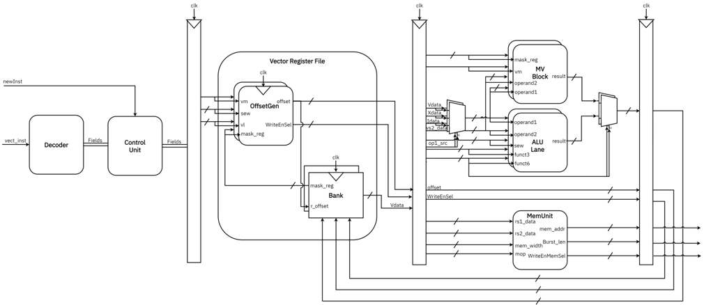
Figure 1: Arrow Datapath
<details>
<summary>Image 1 Details</summary>
### Visual Description
## Block Diagram: Vector Processing Unit
### Overview
The image is a block diagram illustrating the architecture of a vector processing unit. It shows the flow of data and control signals between different components, including a decoder, control unit, vector register file, MV Block, ALU Lane, and memory unit. The diagram emphasizes the parallel processing capabilities inherent in vector operations.
### Components/Axes
* **Decoder:** Receives `vect_inst` as input and outputs `Fields`.
* **Control Unit:** Receives `newInst` and `Fields` as input and outputs `Fields`.
* **Vector Register File:** Contains `OffsetGen` and `Bank`.
* **OffsetGen:** Receives `vm`, `sew`, `vl`, and `mask_reg` as inputs and outputs `offset` and `WriteEnSel`.
* **Bank:** Receives `mask_reg` and `r_offset` as inputs and outputs `Vdata`.
* **MV Block:** Receives `mask_reg`, `vm`, `operand2`, and `operand1` as inputs and outputs `result`.
* **ALU Lane:** Receives `operand1`, `operand2`, `sew`, `funct3`, and `funct6` as inputs and outputs `result`.
* **MemUnit:** Receives `rs1_data`, `rs2_data`, `mem_width`, and `mop` as inputs and outputs `mem_addr` and `Burst_len` and `WriteEnMemSel`.
* **Data Signals:** `Vdata`, `Xdata`, `Idata`, `vs2 data`, `op1_src`, `offset`, `WriteEnSel`.
* **Clock Signals:** `clk` is present at multiple locations, indicating synchronous operation.
### Detailed Analysis
* **Decoder and Control Unit:** The decoder receives a vector instruction (`vect_inst`) and translates it into control signals (`Fields`) for the control unit. The control unit, in turn, generates further control signals based on the decoded instruction and a `newInst` signal.
* **Vector Register File:** This component stores vector data. It contains an `OffsetGen` block, which calculates memory offsets based on inputs like `vm`, `sew`, `vl`, and `mask_reg`. The `Bank` block likely represents the actual memory storage within the register file, receiving `mask_reg` and `r_offset` and outputting `Vdata`.
* **MV Block and ALU Lane:** These are the processing units. The MV Block performs vector operations, receiving operands and a mask (`mask_reg`) to selectively apply the operation. The ALU Lane performs arithmetic and logical operations, receiving operands, `sew` (likely specifying data width), and function codes (`funct3`, `funct6`).
* **MemUnit:** This unit handles memory access. It receives data addresses (`rs1_data`, `rs2_data`), memory width (`mem_width`), and operation codes (`mop`) to perform read/write operations. It outputs the memory address (`mem_addr`), burst length (`Burst_len`), and a write enable signal (`WriteEnMemSel`).
* **Data Flow:** Data flows from the Vector Register File to the MV Block and ALU Lane. The results from these units are then combined through a multiplexer before being sent to the MemUnit and back to the Vector Register File.
### Key Observations
* The diagram highlights the parallel nature of vector processing, with multiple data paths and processing units.
* The `mask_reg` signal is used in both the Vector Register File and the MV Block, indicating its importance in controlling vector operations.
* The presence of `clk` signals throughout the diagram suggests a synchronous design.
### Interpretation
The block diagram illustrates a typical architecture for a vector processing unit. The decoder and control unit handle instruction fetching and decoding, while the vector register file stores the vector data. The MV Block and ALU Lane perform the actual vector operations, and the MemUnit handles memory access. The use of masking and data width signals (`mask_reg`, `sew`) allows for flexible and efficient vector processing. The diagram emphasizes the parallel processing capabilities of the architecture, which are essential for achieving high performance in vector computations.
</details>
register file [27]. VIPERS [28] was another VIRAM-inspired SVP that was designed as a general-purpose accelerator. It included a configurable multi-lane datapath and memory interface. Later SVPs introduced new features like using a scratchpad memory as a vector register file [4], and implementing 2D and 3D vector instructions [22]. Most of these features are incorporated in at least one commercial SVP [23].
through RTL and instruction set simulation. An earlier version of the co-processor targeting embedded applications was implemented in an Intel Cyclone V FPGA and could operate at 50 MHz [13]. Finally, Sapienza University of Rome's Klessydra-T13 [24] is a RISC-V multi-threaded processor with a configurable vector unit. It uses custom vector instructions that replicate some of the basic operations of the standard RVV extension and implement specialized functions for machine learning workloads.
## 3 ARROWARCHITECTURE
Arrow is a configurable vector co-processor that implements a subset of the RVV v0.9 ISA extension. Some of its architectural parameters can be configured at design time including the number of lanes, maximum vector length ( 𝑉𝐿𝐸𝑁 ), and maximum vector element width ( 𝐸𝐿𝐸𝑁 ). In this paper we report on a dual-lane Arrow architecture with 𝑉𝐿𝐸𝑁 = 256 bits and 𝐸𝐿𝐸𝑁 = 64 bits. The current implementation does not support chaining.
The emergence of the RISC-V ISA in 2010 coincided with the proliferation of deep machine learning algorithms and renewed interest in accelerating machine learning training and inference using domain-specific architectures. Berkeley's Hwacha vector architecture [15] inspired the development of a standard RISC-V vector extension (RVV) [19]. Today, a number of commercial products and academic projects are based on implementations of the RVV ISA extension.
## 3.1 Arrow RISC-V Vector ISA Subset
The RISC-V vector extension provides a rich set of vector instructions. Arrow implements a subset of these instructions that we believe can be useful in edge machine learning inference applications. These include unit-stride and strided memory access; single-width integer addition, subtraction, multiplication, and division; bitwise logic and shift; and integer compare, min/max, merge, and move operations.
## 3.2 Pipeline Organization
Figure 1 shows Arrow's datapath. It is a single-issue, dual-lane vector accelerator that can execute two independent vector instructions in parallel. It is pipelined to increase execution throughput, and its pipeline stages include decode, operand fetch, execute or memory access, and write-back.
The Andes NX27V and SiFive VIS7 [5, 11] are commercial processors based on the RVV v1.0 extension. They can operate on 512-bit vectors and are aimed at data-intensive applications in telecommunications, image/video processing, and machine learning. ETH Zurich's Ara is a vector co-processor for the 64-bit Ariane RISC-V processor that is based on the RVV v0.5 ISA extension [3]. It is a scalable architecture that was implemented in 22 nm FD-SOI technology and could operate at 1 GHz+. Four instances of the coprocessor were implemented with 2, 4, 8, and 16 lanes, respectively. Performance results demonstrated the efficiency of the architecture on data-parallel workloads. Ara's support for double-precision floating-point operations makes it well suited for HPC-class dataparallel applications. The University of Southampton's AVA is a RVV co-processor for the OpenHW Group CV32E40P that is optimized for machine learning inference [12]. It implements a subset of the RVV v0.8 ISA extension, uses 32, 32-bit vector registers, and can operate on 8-, 16-, or 32-bit vector elements in SIMD fashion. The AVA co-processor is implemented in Verilog and was validated
Instructions are dispatched from a scalar host processor and are first decoded. Different instruction fields are extracted and fed into the control unit, which generates the appropriate control signals. An offset generator calculates the vector register offsets needed to access the corresponding vector elements. These offsets are sent to the vector register file banks to read the required data. Operands are selected based on the control signals, and depending on the instruction type, the required fields are fed to the ALU, move block, or memory unit. For vector load instructions, the appropriate vector elements are passed to the memory interface, and for arithmetic or logical instructions, results are written back to the register file. The move block executes regular and masked merge and move instructions.
## 3.3 Decoder and Controller
The decoder is a combinational circuit that decomposes the 32-bit instruction it receives from the scalar processor into the appropriate fields needed by other datapath components. The controller uses these fields to generate the appropriate control signals for each vector lane. It also passes control signals and dispatches instructions for execution in the appropriate lane based on the destination vector register. For our dual-lane architecture, if the destination register corresponds to registers 0 to 15 the vector instruction is executed in the first lane. Similarly, if the destination register corresponds to registers 16 to 31 the instruction is executed in the second lane. This lane-dispatching scheme simplifies our design and eliminates the need for complex arbitration hardware. It also supports wider lane implementations, but requires the compiler or assembly programmer to expose vector instruction parallelism through register allocation in a manner similar to statically scheduled superscalar processors. Once generated, control signals are held constant for the duration of a vector instruction execution.
## 3.4 Vector Register File
Arrow's register file is based on a banked architecture where each bank is associated with a different lane. In the current implementation, the first bank contains registers 0 to 15 while the second bank contains registers 16 to 31. Each bank has two read ports and one write port. This enables both banks to support the two lanes simultaneously.
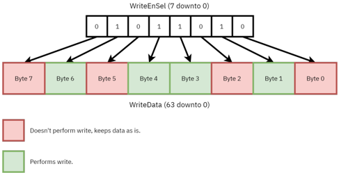
Within Arrow, vector data is processed in 𝐸𝐿𝐸𝑁 -bit words. An offset generator associated with each register bank is used to generate the byte offsets for accessing the corresponding 𝐸𝐿𝐸𝑁 -bit words from a vector register. The offset generator also generates a write-enable selector mask that specifies which bytes within an 𝐸𝐿𝐸𝑁 -bit word should be updated when a result is written back to a vector register. The number of bytes associated with a vector element is determined by the 𝑆𝐸𝑊 parameter, and ⌈ 𝑉𝐿𝐸𝑁 / 𝐸𝐿𝐸𝑁 ⌉ offsets are generated for each vector register. Figure 2 shows how the write-enable selector bits can be used to mask the write back to arbitrary bytes in an 𝐸𝐿𝐸𝑁 -bit word.
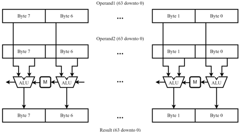
## 3.5 SIMD ALU
The Arrow ALU operates on 𝐸𝐿𝐸𝑁 -bit words regardless of the actual standard element width ( 𝑆𝐸𝑊 ) being used. When 𝑆𝐸𝑊 is less
Figure 2: The WriteEnable bits mapping
<details>
<summary>Image 2 Details</summary>
### Visual Description
## Diagram: Write Enable Selection
### Overview
The image illustrates a write enable selection mechanism for a 64-bit data bus, where individual bytes can be selectively written based on an 8-bit enable signal. The diagram shows how each bit of the `WriteEnSel` signal corresponds to a byte in the `WriteData` bus, determining whether a write operation is performed on that specific byte.
### Components/Axes
* **WriteEnSel (7 downto 0):** An 8-bit signal represented by a row of 8 boxes, each containing a binary digit (0 or 1). This signal controls the write enable for each byte of the `WriteData` bus.
* **WriteData (63 downto 0):** A 64-bit data bus represented by a row of 8 boxes, each labeled "Byte X" (where X ranges from 7 to 0). The color of each box indicates whether a write operation is performed on that byte.
* **Arrows:** Arrows connect each bit of the `WriteEnSel` signal to the corresponding byte in the `WriteData` bus, indicating the control relationship.
* **Legend (Bottom-Left):**
* Red box: "Doesn't perform write, keeps data as is."
* Green box: "Performs write."
### Detailed Analysis
* **WriteEnSel Values:** From left to right, the `WriteEnSel` bits are: 0, 1, 0, 1, 1, 0, 1, 0.
* **WriteData Byte Colors:**
* Byte 7: Red (Doesn't perform write)
* Byte 6: Green (Performs write)
* Byte 5: Red (Doesn't perform write)
* Byte 4: Green (Performs write)
* Byte 3: Green (Performs write)
* Byte 2: Red (Doesn't perform write)
* Byte 1: Green (Performs write)
* Byte 0: Red (Doesn't perform write)
### Key Observations
The diagram clearly shows a one-to-one correspondence between the `WriteEnSel` bits and the `WriteData` bytes. A '1' in the `WriteEnSel` signal enables the write operation for the corresponding byte, while a '0' disables it, preserving the existing data.
### Interpretation
The diagram illustrates a byte-level write enable mechanism. This is a common technique in memory systems and data processing where it's necessary to selectively update portions of a larger data structure. The `WriteEnSel` signal acts as a mask, allowing specific bytes to be modified while leaving others untouched. The alternating pattern of write enables (0, 1, 0, 1, 1, 0, 1, 0) suggests a possible use case where only specific bytes within a 64-bit word need to be updated, potentially for efficiency or data integrity reasons.
</details>
than 𝐸𝐿𝐸𝑁 , the ALU processes multiple vector elements simultaneously in SIMD fashion. Figure 3 shows the Arrow SIMD ALU, which performs basic arithmetic and logic operations. Depending on the actual size of a vector element ( 𝑆𝐸𝑊 ), multiplexers (denoted by M in the Figure) ensure proper carry chain propagation.
<details>
<summary>Image 3 Details</summary>
### Visual Description
## Diagram: 64-bit Operation Diagram
### Overview
The image is a diagram illustrating a 64-bit operation, likely within a processor or similar digital system. It shows how two 64-bit operands are processed byte-by-byte using Arithmetic Logic Units (ALUs) and an 'M' component, presumably representing memory or a multiplexer. The diagram highlights the parallel processing of bytes to produce a 64-bit result.
### Components/Axes
* **Operands:**
* Operand1 (63 downto 0): Represents the first 64-bit input. It is divided into bytes labeled Byte 7, Byte 6, ..., Byte 1, Byte 0.
* Operand2 (63 downto 0): Represents the second 64-bit input, also divided into bytes labeled Byte 7, Byte 6, ..., Byte 1, Byte 0.
* **Processing Units:**
* ALU: Arithmetic Logic Unit, the core processing element.
* M: A component labeled 'M', likely representing memory or a multiplexer. It sits between the ALUs.
* **Result:**
* Result (63 downto 0): The 64-bit output of the operation, divided into bytes labeled Byte 7, Byte 6, ..., Byte 1, Byte 0.
* **Connectors:**
* Lines with arrowheads indicate the flow of data between components.
### Detailed Analysis
The diagram can be broken down into two identical halves, processing bytes 7-6 and bytes 1-0 respectively.
* **Top:** Two input operands, Operand1 and Operand2, each 64 bits wide, are shown. Each operand is divided into 8 bytes (Byte 7 to Byte 0).
* **Middle:** Each corresponding byte from Operand1 and Operand2 is fed into an ALU. The output of the ALUs is then connected to the 'M' component.
* **Bottom:** The output of the 'M' component and the ALUs combine to form the Result (63 downto 0), which is also divided into 8 bytes (Byte 7 to Byte 0).
Specifically:
* Byte 7 of Operand1 and Byte 7 of Operand2 are inputs to an ALU.
* Byte 6 of Operand1 and Byte 6 of Operand2 are inputs to an ALU.
* Byte 1 of Operand1 and Byte 1 of Operand2 are inputs to an ALU.
* Byte 0 of Operand1 and Byte 0 of Operand2 are inputs to an ALU.
The outputs of the ALUs are connected to the 'M' component. The final result is constructed from the outputs of the ALUs and the 'M' component.
### Key Observations
* The diagram suggests a parallel processing architecture where bytes of the operands are processed simultaneously.
* The 'M' component likely plays a role in handling carry or other inter-byte dependencies.
* The "63 downto 0" notation indicates that the most significant bit is bit 63, and the least significant bit is bit 0.
### Interpretation
The diagram illustrates a 64-bit operation performed by breaking down the operands into bytes and processing them in parallel using ALUs. The 'M' component likely handles carry propagation or other inter-byte dependencies to ensure the correct result. This architecture allows for faster processing compared to a serial approach. The diagram is a high-level representation and does not specify the exact nature of the operation performed by the ALUs or the function of the 'M' component.
</details>
Result (63 downto 0)
Figure 3: SIMD ALU Design
## 3.6 Memory Unit
The RVV ISA extension supports different vector memory addressing modes including unit stride, strided, and indexed access. The Arrow memory unit is designed to support these addressing modes by generating corresponding memory addresses. When executing a vector memory instruction, the base address is received from the scalar processor through the rs1\_data port. The memory unit then generates the corresponding effective memory addresses and burst length. The latter is used to determine the number of 𝐸𝐿𝐸𝑁 -bit words that need to be transferred from memory, thus allowing efficient multi-beat bursts. For vector load instructions, the memory unit also generates the WriteEnMemSel bit mask to indicate which vector element bytes should be written in the vector register file. Currently, both unit-stride and strided accesses are fully supported, but vector indexed/gather-scatter access is still in development.
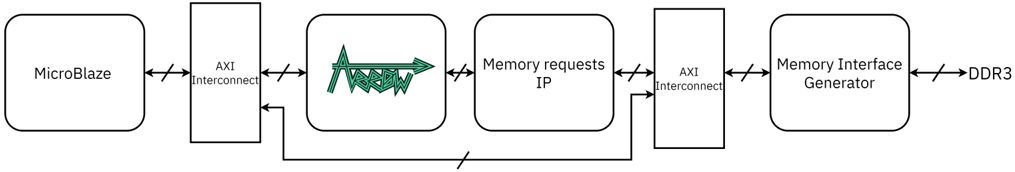
## 3.7 Memory Bus Interface
Because we are using Xilinx design tools, our Arrow system architecture is based on the ARM AMBA AXI bus interface and AXI
Figure 4: FPGA system block diagram. System bus is 𝐸𝐿𝐸𝑁 =64-bits wide.
<details>
<summary>Image 4 Details</summary>
### Visual Description
## Block Diagram: Memory System Architecture
### Overview
The image is a block diagram illustrating a memory system architecture. It shows the flow of data and control signals between different components, including a MicroBlaze processor, AXI interconnects, a memory requests IP block, a memory interface generator, and DDR3 memory.
### Components/Axes
* **MicroBlaze:** A processor block on the left.
* **AXI Interconnect:** Two blocks labeled "AXI Interconnect," one on either side of the "Memory requests IP" block.
* **Memory requests IP:** A block in the center labeled "Memory requests IP."
* **Memory Interface Generator:** A block on the right labeled "Memory Interface Generator."
* **DDR3:** A label on the far right, representing the DDR3 memory.
* **Arrows:** Arrows indicate the direction of data flow between the blocks. Double-headed arrows indicate bidirectional communication. A large, stylized green arrow is present within one of the blocks.
* **Slash Marks:** Slash marks on the arrows indicate multiple signals or a bus.
### Detailed Analysis or ### Content Details
1. **MicroBlaze to AXI Interconnect:** A bidirectional arrow connects the MicroBlaze processor to the first AXI Interconnect block.
2. **AXI Interconnect to Arrow Block:** A bidirectional arrow connects the first AXI Interconnect block to a block containing a stylized green arrow.
3. **Arrow Block to Memory requests IP:** A bidirectional arrow connects the arrow block to the "Memory requests IP" block.
4. **Memory requests IP to AXI Interconnect:** A bidirectional arrow connects the "Memory requests IP" block to the second AXI Interconnect block.
5. **AXI Interconnect to Memory Interface Generator:** A bidirectional arrow connects the second AXI Interconnect block to the "Memory Interface Generator" block.
6. **Memory Interface Generator to DDR3:** A bidirectional arrow connects the "Memory Interface Generator" block to the DDR3 memory.
7. **Feedback Loop:** A line connects the output of the first AXI Interconnect block back to the input of the "Memory requests IP" block, forming a feedback loop.
### Key Observations
* The diagram shows a typical memory system architecture with a processor, interconnects, memory controller, and memory.
* The AXI interconnects facilitate communication between the different components.
* The "Memory requests IP" block likely handles memory request arbitration and scheduling.
* The "Memory Interface Generator" block generates the necessary signals to interface with the DDR3 memory.
* The feedback loop suggests that the "Memory requests IP" block receives information from the AXI Interconnect, possibly related to memory access status or control signals.
### Interpretation
The diagram illustrates a memory system architecture commonly found in embedded systems. The MicroBlaze processor initiates memory requests, which are then routed through the AXI interconnect to the "Memory requests IP" block. This block likely manages the requests and forwards them to the "Memory Interface Generator," which translates the requests into the appropriate signals for the DDR3 memory. The feedback loop allows the "Memory requests IP" block to monitor the status of memory accesses and adjust its scheduling accordingly. The stylized arrow block is likely a placeholder for a more specific component or function within the memory system.
</details>
IPs [1]. Figure 4 shows a high-level view of the memory interface, which includes the Arrow memory unit, Arrow AXI master interface, Xilinx Memory Interface Generator (MIG) IP block, and DDR3 memory. The DDR3 memory provides a shared address space for both the MicroBlaze and Arrow processors. Our system does not currently use any cache or scratchpad memories.
The Arrow memory interface is designed to be system-bus independent. However, in the current implementation, some limitations of the MIG interface can impact performance. For example, the MIG interface is limited to 64-bit transfers. Although this matches Arrow's internal 𝐸𝐿𝐸𝑁 -bit word length, the MIG interface does not support concurrent or interleaved AXI memory transfers. This limits vector memory transfers on the Arrow side to a single lane, which can increase latency and reduce throughput. On the other hand, because the 16-bit MIG/DDR3 interface can operate at 400 MHz, roughly four times the speed of the Arrow core, we can read or write an 𝐸𝐿𝐸𝑁 -bit word every AXI bus cycle.
Within Arrow, the memory unit generates the addresses of required 𝐸𝐿𝐸𝑁 -bit memory words. It also determines the number of memory words that need to be transferred - we refer to these as the number of beats or the burst length. In our current implementation, all memory accesses are 𝐸𝐿𝐸𝑁 =64 bits wide regardless of whether the entire data are needed or not. This simplifies the memory interface and avoids narrow transactions that are smaller than the AXI bus width. For strided vector load instructions, the memory unit also generates the masks that enable the writing of specific bytes to the vector register file. Arrow's AXI master interface is shown as the Memory Requests IP block in Figure 4. It translates an Arrow memory request to an AXI bus transaction. The MIG IP block is external to the Arrow architecture. It serves as a DDR3 memory controller that converts Arrow memory transactions over the AXI bus to DDR3 memory transactions. It also provides the MicroBlaze processor with access to DDR3 memory.
## 4 EXPERIMENTAL METHODOLOGY
In this section we describe our experimental methodology, which includes our FPGA prototype, the code development tools we used, and the fundamental machine learning vector and matrix benchmarks we used to evaluate performance.
## 4.1 FPGA Prototype
After developing the Arrow microarchitecture in VHDL, we synthesized and implemented our design in the Xilinx XC7A200T1SBG484C FPGA used in the Nexys Video board [6]. We also used the Xilinx Vivado 2019.1 Design Suite for synthesis and implementation.
Figure 4 shows our FPGA system implementation. The Arrow datapath is packaged as an AXI IP to enable communication with the MicroBlaze processor and memory over the AXI bus. We chose the Xilinx MicroBlaze v11.0 [25] as our scalar processor because of its compatibility with the Vivado 2019.1 design suite and AXI bus interface. This enabled us to run C test code and send Arrow instructions through the AXI bus. We also validated Arrow's internal signals using the Integrated Logic Analyzer (ILA) IP block, which is available through the Vivado Design Suite. We also developed a standalone IP block that translates Arrow memory requests to AXI bus transactions to ensure the Arrow IP block remained as generic and bus-independent as possible. The DDR3 memory and MIG interface are shared by both the MicroBlaze and Arrow processors.
## 4.2 Code Development Tools
To help us cross-compile benchmark programs written in C/C++, we used the RISC-V LLVM/Clang toolchain from the European Processor Initiative (EPI) project [7], which supported the RVV v0.9 ISA extension specification. Although LLVM/Clang supports the use of RVV instrinsics, we used assembly code inlining to have greater control over our code. We then packaged the inlined code in functions that we used in our benchmarks.
To validate the functionality of our benchmarks, we used the open-source Spike RISC-V ISA simulator [20]. In addition to supporting the base RISC-V instruction set, Spike supports most of the standard ISA extensions including the "V" vector extension. However, because Spike is not cycle-accurate [10], we developed our own cycle count models to evaluate and compare the execution performance of both the scalar and vector benchmarks. To validate our cycle count model, we compared its cycle counts for the scalar benchmark to those produced by Spike and found them to be within 7%.
## 4.3 Benchmarks
To evaluate our design, we used a suite of vector and matrix benchmarks from the University of Southampton [17]. We chose these benchmarks because they are widely used in machine learning inference algorithms, and because they exhibit high levels of data parallelism. The benchmarks include vector addition, multiplication, max reduction, dot product, and rectified linear unit (ReLu).
Table 1: Benchmark Parameters
| | Small Data Profile | Medium Data Profile | Large Data Profile |
|--------------------------|----------------------|-----------------------|----------------------|
| Vector Length | 64 elements | 512 elements | 4096 elements |
| Matrix Size | 64 × 64 | 512 × 512 | 4096 × 4096 |
| 2D Convolution Data Size | 1024 × 1024 | 1024 × 1024 | 1024 × 1024 |
| Kernel Size | 3 × 3 | 4 × 4 | 5 × 5 |
| Channels | 1 | 1 | 1 |
| Batch Size | 3 | 4 | 5 |
They also include matrix multiplication, addition, max pool, and 2D convolution.
The original benchmark suite was developed for the RVV v0.8 ISA extension specification. To support the RVV v0.9 specification, we made minor adjustments to its inlined assembly code functions. We then compiled the applications using LLVM/Clang and simulated them on Spike for functional validation. Finally, we compared the scalar and vector execution times by applying our cycle count models. We also calculated the energy used by each benchmark by multiplying the power consumed, which we obtained from the FPGA synthesis reports, by the execution time. We calculated a benchmark's execution time by multiplying its cycle count by the Arrow clock cycle time. To study the impact of data size on performance and energy consumption, we also ran our benchmarks with small, medium and large data sizes. Table 1 describes our different data size profiles.
## 5 RESULTS
In this section, we report on the results of implementing the Arrow system in a FPGA device. We also report on the performance and energy of the Arrow accelerator on vector and matrix benchmarks.
## 5.1 FPGA Resource Utilization
To evaluate our design, we synthesized and implemented two systems: one with a single MicroBlaze processor and another with both MicroBlaze and Arrow processors. Both systems ran at 100 MHz. Table 2 summarizes our post-implementation results, which demonstrate the minor increase in LUT and FF utilization, and power consumption, due to the Arrow accelerator. And although we operated Arrow at 100 MHz, its maximum clock speed is 112 MHz.
## 5.2 Benchmark Performance
Table 3 shows the cycle counts for the scalar and vectorized benchmarks for different data size profiles. The Table also shows the speedup factors of vectorized benchmarks relative to scalar benchmarks. Our results show that the vector benchmarks run 25 - 78 × faster; the matrix benchmarks run 5 - 78 × faster; and 2D convolution runs only 1.4 - 1.9 × faster. The relatively low performance of 2D convolution and, to a lesser extent, Matrix Max Pool is mainly due to their highly repetitive use of scalar arithmetic operations to manage data pointers. This greatly limits performance despite both benchmarks using optimized vector reduction and dot product functions, respectively. We believe that strided vector memory operations can improve the performance of both applications, and we are currently working on further optimizing these benchmarks. It is also worth noting that vectorized benchmarks with larger data profiles achieve better performance than those with smaller data profiles. This is mainly due to vector overhead instructions (e.g. setting the vector length) having a lower impact on execution time when vector instructions operate on longer vectors.
These results highlight the performance and energy advantages of the RVV-based Arrow architecture, and validate its suitability for edge machine learning inference applications.
Table 4 shows the energy consumed by the scalar and vectorized benchmarks for different data size profiles. The Table also shows the ratio of energy consumed by vectorized benchmarks relative to corresponding scalar benchmarks. Our results show that the Arrow accelerator achieves significant energy reductions relative to a scalar processor. This is mainly due to the significant reduction in execution time, which directly impacts energy consumption. Comparing the energy consumed by the vectorized benchmarks to that consumed by the scalar benchmarks we find that the vector benchmarks consume 96% to 99% less energy; the matrix benchmarks consume 80% to 99% less energy; and 2D convolution consumes 20% to 43% less energy. While still significant, we believe that further optimizations to 2D convolution and Matrix Max Pool will result in further reductions in energy consumption.
## 6 CONCLUSIONS AND FUTURE WORK
In this paper we described the architecture of our RVV-based Arrow accelerator and evaluated its performance and energy consumption. Our results confirm its suitability for edge machine learning inference applications. We plan to extend this work by evaluating the Arrow accelerator when it is more tightly integrated into the datapath of a RISC-V processor like the SweRV EH1. We also plan to develop a gem5 simulation model to perform a more thorough performance study of the Arrow accelerator using the MLPerf and TinyMLPerf benchmark suites. Finally, we plan to expand the Arrow architecture to support ML-friendly arithmetic operations and data types like bfloat16 and posits.
## REFERENCES
- [1] ARM. [n.d.]. AMBA AXI and ACE Protocol Specification AXI3, AXI4, and AXI4-Lite ACE and ACE-Lite .
- [3] Matheus Cavalcante, Fabian Schuiki, Florian Zaruba, Michael Schaffner, and Luca Benini. 2020. Ara: A 1-GHz+ Scalable and Energy-Efficient RISC-V Vector Processor With Multiprecision Floating-Point Support in 22-nm FD-SOI. IEEE Transactions on Very Large Scale Integration (VLSI) Systems 28, 2 (2020), 530-543. https://doi.org/10.1109/TVLSI.2019.2950087
- [2] Krste Asanovic. 1998. Vector Microprocessors . Ph.D. Dissertation. University of California, Berkeley.
- [4] Christopher H. Chou, Aaron Severance, Alex D. Brant, Zhiduo Liu, Saurabh Sant, and Guy G.F. Lemieux. 2011. VEGAS: Soft Vector Processor with Scratchpad Memory. In Proceedings of the 19th ACM/SIGDA International Symposium on Field Programmable Gate Arrays (Monterey, CA, USA) (FPGA '11) . Association for Computing Machinery, New York, NY, USA, 15-24. https://doi.org/10.1145/ 1950413.1950420
- [6] Digilent. [n.d.]. Nexys Video Reference Manual. [Online]. https://reference. digilentinc.com/reference/programmable-logic/nexys-video/reference-manual
- [5] Mike Demler. 2020. Andes Plots RISC-V Vector Heading: NX27V CPU Supports up to 512-bit Operations. Microprocessor Report May (2020), 4.
- [7] EPI. 2021. LLVM-based Compiler. [Online]. https://repo.hca.bsc.es/gitlab/rferrer/ llvm-epi
- [8] Roger Espasa, Mateo Valero, and James E. Smith. 1998. Vector Architectures: Past, Present and Future. In Proceedings of the 12th International Conference on Supercomputing (Melbourne, Australia) (ICS '98) . Association for Computing Machinery, New York, NY, USA, 425-432. https://doi.org/10.1145/277830.277935
| | Utilization | Utilization | Utilization | Power (W) |
|------------------|--------------------|---------------|---------------|-------------|
| | LUT | FF | BRAM | |
| MicroBlaze | 2241/133800 (1.7%) | 1495/267600 | 32/365 | 0.270 |
| MicroBlaze+Arrow | 2715/133800 (2.0%) | 2268/267600 | 32/365 | 0.297 |
Table 2: FPGA Implementation Results
Table 3: Cycle-Count Performance Analysis
| | Small Data Profile | Small Data Profile | Small Data Profile | Medium Data Profile | Medium Data Profile | Medium Data Profile | Large Data Profile | Large Data Profile | Large Data Profile |
|-----------------------|----------------------|----------------------|----------------------|-----------------------|-----------------------|-----------------------|----------------------|----------------------|----------------------|
| Operation | Scalar (cycles) | Vector (cycles) | Speedup | Scalar (cycles) | Vector (cycles) | Speedup | Scalar (cycles) | Vector (cycles) | Speedup |
| Vector Addition | 3 . 4 × 10 3 | 5 . 0 × 10 1 | 69 . 6 × | 2 . 7 × 10 4 | 3 . 5 × 10 2 | 77 . 3 × | 2 . 2 × 10 5 | 2 . 8 × 10 3 | 78 . 4 × |
| Vector Multiplication | 3 . 5 × 10 3 | 5 . 0 × 10 1 | 69 . 5 × | 2 . 8 × 10 4 | 3 . 6 × 10 2 | 77 . 3 × | 2 . 2 × 10 5 | 2 . 8 × 10 3 | 78 . 3 × |
| Vector Dot Product | 1 . 6 × 10 3 | 6 . 2 × 10 1 | 25 . 2 × | 1 . 2 × 10 4 | 3 . 8 × 10 2 | 32 . 1 × | 9 . 8 × 10 4 | 3 . 0 × 10 3 | 33 . 2 × |
| Vector Max Reduction | 1 . 4 × 10 3 | 4 . 2 × 10 1 | 32 . 6 × | 1 . 1 × 10 4 | 2 . 2 × 10 2 | 48 . 1 × | 8 . 6 × 10 4 | 1 . 7 × 10 3 | 51 . 2 × |
| Vector ReLu | 1 . 4 × 10 3 | 4 . 2 × 10 1 | 34 . 0 × | 1 . 1 × 10 4 | 2 . 9 × 10 2 | 38 . 4 × | 9 . 0 × 10 4 | 2 . 3 × 10 3 | 39 . 0 × |
| Matrix Addition | 2 . 2 × 10 4 | 5 . 1 × 10 3 | 43 . 8 × | 1 . 4 × 10 7 | 2 . 0 × 10 5 | 71 . 6 × | 9 . 1 × 10 8 | 1 . 2 × 10 7 | 77 . 6 × |
| Matrix Multiplication | 1 . 2 × 10 7 | 5 . 1 × 10 5 | 24 . 1 × | 6 . 1 × 10 9 | 1 . 2 × 10 8 | 50 . 4 × | 3 . 1 × 10 12 | 5 . 3 × 10 10 | 58 . 6 × |
| Matrix Max Pool | 3 . 7 × 10 5 | 7 . 0 × 10 4 | 5 . 4 × | 2 . 4 × 10 7 | 4 . 4 × 10 6 | 5 . 4 × | 1 . 5 × 10 9 | 2 . 8 × 10 8 | 5 . 4 × |
| 2D Convolution | 1 . 4 × 10 9 | 7 . 3 × 10 8 | 1 . 9 × | 1 . 9 × 10 9 | 1 . 2 × 10 9 | 1 . 6 × | 2 . 4 × 10 9 | 1 . 8 × 10 9 | 1 . 4 × |
Table 4: Energy Consumption Analysis
| | Small Data Profile | Small Data Profile | Small Data Profile | Medium Data Profile | Medium Data Profile | Medium Data Profile | Large Data Profile | Large Data Profile | Large Data Profile |
|-----------------------|----------------------|----------------------|----------------------|-----------------------|-----------------------|-----------------------|----------------------|----------------------|----------------------|
| Operation | Scalar (J) | Vector (J) | Ratio | Scalar (J) | Vector (J) | Ratio | Scalar (J) | Vector (J) | Ratio |
| Vector Addition | 8 . 6 × 10 - 6 | 1 . 4 × 10 - 7 | 1.6% | 6 . 8 × 10 - 5 | 9 . 7 × 10 - 7 | 1.4% | 5 . 44 × 10 - 4 | 7 . 6 × 10 - 6 | 1.4% |
| Vector Multiplication | 8 . 5 × 10 - 6 | 1 . 3 × 10 - 7 | 1.6% | 6 . 9 × 10 - 5 | 9 . 6 × 10 - 7 | 1.4% | 5 . 3 × 10 - 4 | 7 . 5 × 10 - 6 | 1.4% |
| Vector Dot Product | 3 . 8 × 10 - 6 | 1 . 7 × 10 - 7 | 4.4% | 3 . 0 × 10 - 5 | 1 . 0 × 10 - 6 | 3.4% | 2 . 4 × 10 - 4 | 8 . 0 × 10 - 6 | 3.3% |
| Vector Max Reduction | 3 . 4 × 10 - 6 | 1 . 1 × 10 - 7 | 3.4% | 2 . 6 × 10 - 5 | 6 . 1 × 10 - 7 | 2.3% | 2 . 1 × 10 - 4 | 4 . 5 × 10 - 6 | 2.1% |
| Vector ReLu | 3 . 5 × 10 - 6 | 1 . 1 × 10 - 7 | 3.2% | 2 . 8 × 10 - 5 | 7 . 9 × 10 - 7 | 2.9% | 2 . 2 × 10 - 4 | 6 . 2 × 10 - 6 | 2.8% |
| Matrix Addition | 5 . 52 × 10 - 4 | 1 . 4 × 10 - 5 | 2.5% | 3 . 5 × 10 - 2 | 5 . 4 × 10 - 4 | 1.5% | 2 . 2 × 10 0 | 3 . 2 × 10 - 2 | 1.4% |
| Matrix Multiplication | 3 . 0 × 10 - 2 | 1 . 4 × 10 - 3 | 4.6% | 1 . 5 × 10 1 | 3 . 3 × 10 - 1 | 2.2% | 7 . 6 × 10 3 | 1 . 4 × 10 2 | 1.9% |
| Matrix Max Pool | 9 . 2 × 10 - 4 | 1 . 88 × 10 - 4 | 20.5% | 5 . 9 × 10 - 2 | 1 . 2 × 10 - 2 | 20.4% | 3 . 8 × 10 0 | 7 . 65 × 10 - 1 | 20.4% |
| 2D Convolution | 3 . 4 × 10 0 | 1 . 9 × 10 0 | 57.3% | 4 . 5 × 10 0 | 3 . 2 × 10 0 | 70.4% | 6 . 0 × 10 0 | 6 . 7 × 10 0 | 79.9% |
- [9] John L. Hennessy and David A. Patterson. 2019. A New Golden Age for Computer Architecture. Commun. ACM 62, 2 (Jan. 2019), 48-60. https://doi.org/10.1145/ 3282307
- [22] Aaron Severance and Guy Lemieux. 2012. VENICE: A compact vector processor for FPGA applications. In 2012 International Conference on Field-Programmable Technology . 261-268. https://doi.org/10.1109/FPT.2012.6412146
- [11] Aakash Jani. 2021. SiFive Brings Vectors to S-Series. Microprocessor Report January (2021), 4.
- [10] Vladimir Herdt, Daniel Große, and Rolf Drechsler. 2020. Fast and Accurate Performance Evaluation for RISC-V using Virtual Prototypes*. In 2020 Design, Automation Test in Europe Conference Exhibition (DATE) . 618-621. https://doi. org/10.23919/DATE48585.2020.9116522
- [23] Aaron Severance and Guy G. F. Lemieux. 2013. Embedded Supercomputing in FPGAs with the VectorBlox MXP Matrix Processor. In Proceedings of the Ninth IEEE/ACM/IFIP International Conference on Hardware/Software Codesign and System Synthesis (Montreal, Quebec, Canada) (CODES+ISSS '13) . IEEE Press, Article 6, 10 pages.
- [12] M. Johns, H. Cooper, P. Alexander, A. Bhattacharya, B. Theobald, and J. Holden. 2021. Expanding a RISC-V Processor with Vector Instructions for Accelerating Machine Learning. https://youtu.be/t0Fpy4TzLUE
- [14] C.E. Kozyrakis and D.A. Patterson. 2003. Scalable, vector processors for embedded systems. IEEE Micro 23, 6 (2003), 36-45. https://doi.org/10.1109/MM.2003.1261385
- [13] Matthew Johns and Tom J. Kazmierski. 2020. A Minimal RISC-V Vector Processor for Embedded Systems. In 2020 Forum for Specification and Design Languages (FDL) . 1-4. https://doi.org/10.1109/FDL50818.2020.9232940
- [15] Yensup Lee. 2016. Decoupled Vector-Fetch Architecture with a Scalarizing Compiler . Ph.D. Dissertation. University of California, Berkeley.
- [17] University of Southampton. 2021. AI-Vector-Accelerator Benchmarks. [Online]. https://github.com/AI-Vector-Accelerator/NN\_software
- [16] E. McLellan. 1993. The Alpha AXP architecture and 21064 processor. IEEE Micro 13, 3 (1993), 36-47. https://doi.org/10.1109/40.216747
- [18] David Patterson and Andrew Waterman. 2017. SIMD Instructions Considered Harmful. https://www.sigarch.org/simd-instructions-considered-harmful
- [20] RISC-V. 2021. Spike, a RISC-V ISA Simulator. [Online]. https://github.com/riscv/ riscv-isa-sim
- [19] RISC-V. 2021. RISC-V Vector Extension, v0.9. [Online]. https://github.com/riscv/ riscv-v-spec/releases/tag/0.9
- [21] Richard M. Russell. 1978. The CRAY-1 Computer System. Commun. ACM 21, 1 (Jan. 1978), 63-72. https://doi.org/10.1145/359327.359336
- [25] Xilinx. 2020. Xilinx MicroBlaze Processor Reference Guide. [Online]. https://www.xilinx.com/support/documentation/sw\_manuals/xilinx2018\_ 2/ug984-vivado-microblaze-ref.pdf
- [24] S. Sordillo, A. Cheikh, A. Mastrandrea, F. Menichelli, and M. Olivieri. 2021. Customizable Vector Acceleration in Extreme-Edge Computing: A RISC-V Software/Hardware Architecture Study on VGG-16 Implementation. Electronics 10, 518 (2021), 21. https://doi.org/10.3390/electronics10040518
- [26] Peter Yiannacouras, J. Gregory Steffan, and Jonathan Rose. 2008. Vespa: Portable, scalable, and flexible fpga-based vector processors. In In CASES'08: International Conference on Compilers, Architecture and Synthesis for Embedded Systems .
- [28] Jason Yu, Guy Lemieux, and Christpher Eagleston. 2008. Vector Processing as a Soft-Core CPU Accelerator. In Proceedings of the 16th International ACM/SIGDA Symposium on Field Programmable Gate Arrays (Monterey, California, USA) (FPGA '08) . Association for Computing Machinery, New York, NY, USA, 222-232. https: //doi.org/10.1145/1344671.1344704
- [27] Peter Yiannacouras, J. Gregory Steffan, and Jonathan Rose. 2009. Fine-Grain Performance Scaling of Soft Vector Processors. In Proceedings of the 2009 International Conference on Compilers, Architecture, and Synthesis for Embedded Systems (Grenoble, France) (CASES '09) . Association for Computing Machinery, New York, NY, USA, 97-106. https://doi.org/10.1145/1629395.1629411