## A 64-core mixed-signal in-memory compute chip based on phase-change memory for deep neural network inference
Manuel Le Gallo, 1,2, a) Riduan Khaddam-Aljameh, 1,2 Milos Stanisavljevic, 1,2 Athanasios Vasilopoulos, 2 Benedikt Kersting, 2 Martino Dazzi, 2 Geethan Karunaratne, 2 Matthias Br¨ andli, 2 Abhairaj Singh, 2 Silvia M. M¨ uller, 3 Julian B¨ uchel, 2 Xavier Timoneda, 2 Vinay Joshi, 2 Urs Egger, 2 Angelo Garofalo, 2 Anastasios Petropoulos, 4 Theodore Antonakopoulos, 4 Kevin Brew, 5 Samuel Choi, 5 Injo Ok, 5 Timothy Philip, 5 Victor Chan, 5 Claire Silvestre, 5 Ishtiaq Ahsan, 5 Nicole Saulnier, 5 Vijay Narayanan, 6 Pier Andrea Francese, 2 Evangelos Eleftheriou, 2 and Abu Sebastian 2, b)
1) These authors contributed equally
2) IBM Research Europe, 8803 R¨ uschlikon, Switzerland
3) IBM Systems and Technology, 71034 B¨ oblingen, Germany
4) University of Patras, 26504 Rio Achaia, Greece
5) IBM Research - Albany, NY 12203, USA
6) IBM Research - Yorktown Heights, NY 10598, USA
(Dated: 7 December 2022)
The need to repeatedly shuttle around synaptic weight values from memory to processing units has been a key source of energy inefficiency associated with hardware implementation of artificial neural networks 1 . Analog in-memory computing (AIMC) with spatially instantiated synaptic weights holds high promise to overcome this challenge, by performing matrix-vector multiplications (MVMs) directly within the network weights stored on a chip to execute an inference workload 2-7 . However, to achieve end-to-end improvements in latency and energy consumption, AIMC must be combined with on-chip digital operations and communication to move towards configurations in which a full inference workload is realized entirely on-chip. Moreover, it is highly desirable to achieve high MVM and inference accuracy without application-wise re-tuning of the chip. Here, we present a multi-core AIMC chip designed and fabricated in 14-nm complementary metal-oxide-semiconductor (CMOS) technology with backend-integrated phase-change memory (PCM). The fully-integrated chip features 64 256x256 AIMC cores interconnected via an on-chip communication network. It also implements the digital activation functions and processing involved in ResNet convolutional neural networks and long short-term memory (LSTM) networks. We demonstrate near software-equivalent inference accuracy with ResNet and LSTM networks while implementing all the computations associated with the weight layers and the activation functions on-chip. The chip can achieve a maximal throughput of 63.1 TOPS at an energy efficiency of 9.76 TOPS W -1 for 8-bit input/output matrix-vector multiplications.
Early works on performing neural network inference with AIMC showed promising accuracy results in mixed hardware/software implementations, where functionalities such as digital-to-analog and analog-to-digital conversions, activation functions, and other necessary digital operations were implemented with off-chip software or hardware 8-12 . Since then, various single- or few-core chips using SRAM 13 , Flash 14 , RRAM 15-17 , PCM 18 , and MRAM 19 memory technologies have been fabricated with fully-integrated data conversions and sometimes activation functions 14,15,18 , demonstrating a competitive energy efficiency of ≥ 10 TOPS W -1 for reduced-precision MVM. In such works, only small networks ( 100k weights) on simple benchmark tasks such as MNIST digit recognition have been implemented to fit entirely on the core 14-18 , whereas larger networks have been emulated by programming each layer one at a time onto the same core 13,19 . Recently, multi-core chips supporting larger networks ( > 1M weights) have demonstrated promising inference accuracy results on more difficult benchmarks, such as image recognition on the CIFAR dataset, and high MVM energy efficiency 20-25 .
Despite those advances, significant challenges remain to build a complete AIMC accelerator to demonstrate end-to-end inference tasks with accuracy and efficiency that outperform the already existing digital accelerators. Because of the rather large size of the multi-bit SRAM plus switched-capacitor unit-cells, the existing SRAM-based implementations need off-chip weight buffers to hold network weights, which are then partially transferred to the AIMC cores because an entire network cannot fit fully on-chip 24 . The current implementations are not dense enough to hold > 10MB of weight data at reasonable chip area, limiting their efficiency gains over digital approaches to rather small networks that fit entirely on-chip 1 . Another limitation is the volatility of the SRAM cells, which prevent the on-chip weights to be retained throughout power cycling of the accelerator.
The potential to achieve smaller unit-cell sizes with resistive memory technologies could make it possible to hold such large networks entirely on-chip in a non-volatile way and eliminate the overhead of off-chip weight data access. In this context, an AIMC accelerator based on such devices becomes a natural choice. Both digital 20,22 (1 device corresponds to 1 weight bit) and analog (1 device encodes an entire weight) 21,25 storage of weights in those devices have been explored in the recent AIMC
a) Electronic mail: anu@zurich.ibm.com
b) Electronic mail: ase@zurich.ibm.com
chips. Digital storage offers high accuracy, but the throughput is limited due to the small number of rows that can be operated at a time (sometimes as low as 4) 22 without degrading the signal quality, in order to prevent large errors when processing the most significant bits. This approach also limits the achievable weight density because several devices are needed to encode a weight. Analog weight storage offers high weight density and the ability to operate more rows simultaneously (demonstrated up to 512) 25 . However, this approach suffers from accuracy degradation because of the noisy analog weights and higher latency due to the need of slow high resolution analog-to-digital converters (ADCs) that often have to be multiplexed across columns. Moreover, extensive network-specific chip tuning, such as per-network recalibration of the chip to mitigate non-idealities of the devices and peripheral circuitry, and chip-in-the-loop finetuning of weights through backpropagation, has so far been necessary to achieve acceptable inference accuracy with this approach 11,21 . Finally, at the system level, none of the current AIMC chips based on resistive memory support all the computations involved in processing convolutional and LSTM layers.
To address those challenges, we present the IBM HERMES Project Chip: a 64-core AIMC chip based on back-end integrated PCM in a 14-nm CMOS process. The chip delivers simultaneously four key advances over the previous implementations discussed above. (i) High weight capacity is enabled through the analog storage capability of PCM, using only 4 PCM devices to encode a weight. (ii) Low MVM latency, high parallelism, and high throughput are achieved by using compact current-controlled oscillator ADCs placed on each unit-cell row to perform fully-parallel MVMs. (iii) High MVM and inference accuracy are achieved without application-wise chip re-tuning, thanks to proper on-chip ADC calibration circuits that remove unwanted nonlinear response. (iv) Finally, all non-MVM computations involved in processing convolutional and LSTM layers are supported using dedicated high-precision digital units. We report measured inference results at near software-equivalent accuracy on CIFAR-10 image recognition, Penn Treebank (PTB) character prediction, and image caption generation tasks with all convolutional and LSTM layer computations performed on-chip. The measured MVM throughput per area of the chip is > 15 × higher than comparable multi-core resistive memory AIMC chips, while achieving the highest accuracy on the CIFAR-10 benchmark.
## I. CHIP ARCHITECTURE
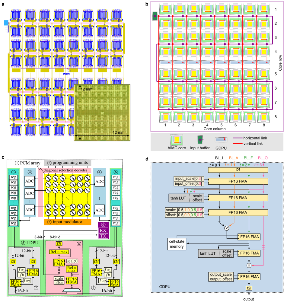
Fig. 1a shows a snapshot of the chip inside the electronic design automation (EDA) tool. The chip has a square dimension of 12mm × 12mm. Its 64 cores, each of size 1 . 2mm × 1 . 16mm, are placed in eight rows and eight columns. This subdivided structure is detailed in the schematic illustration in Fig. 1b. Each core contains a PCM crossbar array capable of storing a 256 × 256 weight matrix and performing an analog MVM using the input activations provided from outside of the core. Hence, up to 4,194,304 weights can be stored on-chip for performing in-memory MVMs.
At the center of the core grid, between rows four and five, a row of eight global digital processing units (GDPUs) is placed. They provide the additional digital post-processing capabilities needed when running LSTM networks. The high-frequency clock signals for the digital circuitry in the cores and GDPUs are received at the center of the chip and are distributed in a balanced tree across the chip.
Finally, the core outputs and GDPU inputs are interconnected by a grid of horizontal and vertical digital communication links (see Fig. 1b), yielding a DNN acceleration architecture where weight elements are stationary, and only the activation vectors are transmitted. There are 418 physical communication links in total, which together implement a 5 Parallel Prism communication fabric topology 26 (see Extended Data Fig. 1 for a map of all possible link connections). A summary of the chip specifications can be found in Extended Data Table I.
## II. THE COMPUTATIONAL MEMORY CORE
Fig. 1c depicts the architecture of a single core and its various components. The design is based on the fully-integrated standalone PCM-based single-core chip presented in Ref. 18, with the addition of the link controller for transmitting and receiving data across different cores. At the center of the core, there is a 256 × 256-sized crossbar array of PCM-based unit-cells. As shown in Extended Data Fig. 2a, four PCM devices are used per unit-cell: two each for each polarity, such that positive and negative weights can be represented 27,28 . The phase-configuration of the phase-change material within the mushroom-type PCM devices determine their conductance (see Extended Data Fig. 3). The devices in a conductance pair are weighted with equal significance.
To program the individual conductances, a diagonal decoding scheme 28 is employed to select 256 different devices, one per row and column. The whole procedure starts with the dedicated per-core programming finite-state machine (FSM) instructing the diagonal selection decoder to enable one diagonal of cells that contains the devices that are to be programmed (see Extended Data Fig. 2b). Subsequently, these selected devices can be programmed by the current-steering digital-to-analog converter (DAC) based programming units located on top of the PCM array. The DAC units are capable of producing all required programming pulse shapes for the PCM devices based on the instruction provided by the FSM. This includes high current RESET pulses, triangular-shaped SET pulses, and programming pulses with variable current amplitude and time duration.
Once all programming operations are concluded, the core can be used to perform analog MVMs. To this end, the input modulator applies pulse-width modulated (PWM) read voltage pulses to the PCM array, which are digitized by an array of 256 time-based current-ADCs. These ADCs flank the PCM-array from the left and right side, such that each unit-cell row is associated with a dedicated ADC. This is achieved by matching the ADC height to that of two unit-cells, which results in a skewed aspect ratio, as is shown in the layout in Extended Data Fig. 2c. By choosing a current-based ADC topology, area-intensive and noise-prone current-to-voltage conversion steps can be avoided. Furthermore, by opting for a time-based architecture, a highly digital design is obtained in which the output precision can be adjusted by changing the conversion time.
To counteract manufacturing mismatch and other non-idealities, the ADC includes an internal resistor ladder-based voltage DAC that allows correcting the read-voltage offset. Furthermore, the internal current mirror, which drives the attached currentcontrolled oscillator (CCO) unit, contains trimming registers that allow matching the gain between the different ADCs per core and compensating nonlinearity in their transfer function 18 . Thus, after performing an initial calibration procedure, the configuration parameters are stored on-chip such that the ADCs exhibit tightly distributed and linear transfer curves. Note that this calibration is independent of the deployed application and does not have to be redone for different weight sets or networks.
Extended Data Fig. 4a illustrates one row of the computational memory during an analog MVM. The per-row ADC regulates the bit line (BL) to a fixed common-mode voltage, such that the top electrodes of all PCM devices in the 256 unit-cells are on the same potential. Their respective source line (SL) potentials, however, are connected to one of three potentials based on the respective input value, i.e., the positive read voltage V + to subtract current, the negative read voltage V -when adding current, or high impedance when no current from the cell is to be added. Thus, all combinations of products between a positive or negative weight and a positive or negative input can be performed in the analog domain in a single modulation, as shown in Extended Data Fig. 4b. In addition, a 4-phase mode is supported that is shown in Extended Data Fig. 4c. Therein, the four combination of ± weights and ± inputs are performed in four separate operations while only using the negative read voltage V -. As a result, a higher accuracy of the measured current is achieved, as all PCM devices are read in the same polarity by the current-based ADC. Therefore, all experiments in this work were performed using the higher precision 4-phase mode. Compensation schemes to mitigate the impact of the current-voltage polarity dependence of PCM 29 to enable high precision in the 1-phase mode will be the subject of future investigations.
The ADC delivers the final results as two 12-bit unsigned integers, one for the positive and one for the negative current. By using tri-state buffers on a 24-bit wide bus, the results are transmitted from each ADC to the local digital processing unit (LDPU) for post-processing. In the first step, the results are transferred to a register array, such that the operation becomes fully pipelined. Consequently, the initial latency of the LDPU does not affect its throughput (one data point per clock cycle). Next, the results are transferred one by one to the ADC-convert-and-scale block, which first converts the 12-bit integers to half-precision floatingpoint format ( FP16 ) and then employs two fused multiply-add (FMA) units to remove gain and offset errors.
Two ADC-convert-and-scale blocks produce outputs every second clock cycle and feed them one after the other to the activation function block through a multiplexer unit. There, affine scaling per channel, as well as an optional ReLU operation, are applied. The intermediate value is then combined with an 8-bit signed integer ( INT8 ) input coming from the neighboring cores, or from off-chip, through the link controller receiver (RX). This value is first converted into FP16 format and then scaled to the optimal range. Finally, the output undergoes another optional ReLU operation before conversion into INT8 , ready to be shipped by the transmitter (TX) of the link controller. The existence of both ReLU operations allows the possibility to apply the activation either before or after adding the RX link input. The activation block is fully pipelined so that its latency does not affect the LDPU throughput.
The link controller implements a state machine that enables transmission and reception of data within at most six neighboring cores (receiving and transmitting cores are not necessarily the same, see Extended Data Fig. 1). The core-to-core input-output links are implemented as eight parallel channels, each transferring one bit every clock cycle. The selection of the data source for the TX and of the data destination for the RX is implemented through a routing table, configured before runtime. Specifically, the transmitter-side link controller prepends a preamble to the payload being sent on the links. The preamble contains information to uniquely identify a routing path for a particular type of payload. If the receiving core is enabled to receive data from the transmitting core in the routing table, the link controller samples the incoming data. Furthermore, the link controller in the transmitting and receiving cores can select a portion of the payload according to another set of routing registers. In the current design, the links can transfer data across the LDPUs of multiple cores to realize fully on-chip intra-layer partial sum accumulation, and transfer data from the LDPU to the input of a GDPU.
## III. THE GLOBAL DIGITAL PROCESSING UNIT
The GPDU is responsible for the digital processing required in LSTM networks. The chip contains eight GDPU slices in total, each connected to the fourth row core above a GDPU slice. The cores in a column above a GDPU slice can aggregate their outputs in a cascaded fashion in the LDPUs of those cores. The final aggregated output produced by the LDPU of the fourth row core is then sent to its corresponding GDPU slice. Each slice takes up to 256 inputs serially (one in each clock cycle), out of which 64 inputs of input gate's (I), cell input (A), forget gate's (F), and output gate's (O) pre-activation vector. Those
pre-activation vector inputs arrive in an alternating fashion from four neighbouring BLs. By mapping columns of the I, A, F, and O weight matrices in an interleaved fashion, a single element processor per GDPU slice (instead of 64) can be used to process the 256 inputs serially, which significantly reduces the number of resources needed in the GDPU. Each GDPU slice produces one output every four clock cycles for up to 64 outputs. It also contains cell state memory registers for up to 64 elements.
Fig. 1d depicts one GDPU slice architecture in detail. All computations inside the GDPU slice are performed in the FP16 format with inputs and outputs in INT8 format. Hyperbolic tangent activation functions are realized using a lookup table (LUT) method. First, a bank of 17 comparators is used to find the corresponding bin (out of 18) in which an input is contained. Then, the output value is interpolated in a fused-multiply-add (FMA) unit using the slope and offset read from the LUT for the determined bin. The output activations of the four gates are further processed by two multiply blocks, three FMA blocks, and one more hyperbolic tangent LUT block to compute the cell-state and the hidden state output of the LSTM unit.
## IV. MVM ACCURACY
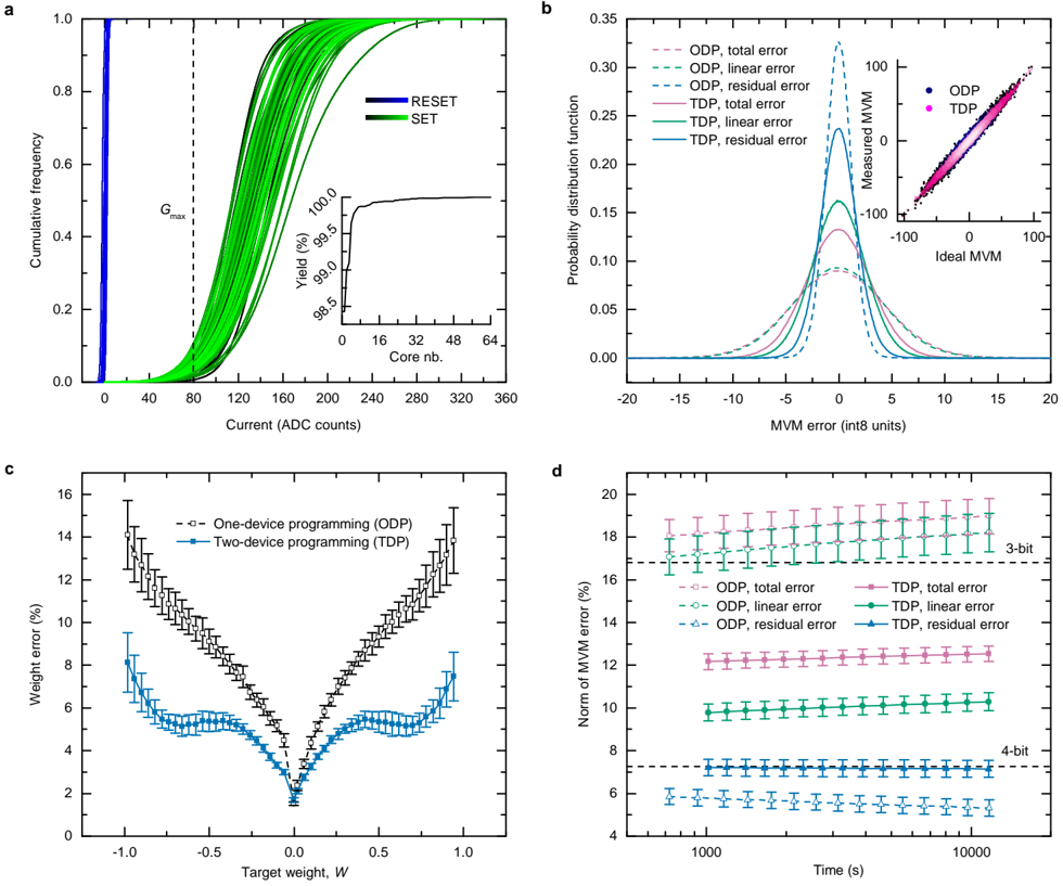
Wecharacterized all 64 cores of a single chip to assess the PCM yield and how accurately MVMs can be performed with them. Fig. 2a shows the SET and RESET distributions of the unit-cells of all 64 cores. The unit-cell comprises four PCM devices (two per polarity). Therefore, we define a unit-cell in the RESET state ( G RESET) when all PCM devices are programmed to RESET, and a unit-cell in the SET state ( G SET) when one PCM device is programmed to SET and the others to RESET. On 63 out of the 64 cores of this chip, more than 99% of the unit cells can be programmed to | G RESET | smaller than 5 ADC counts and G SET larger than 50 ADC counts. The yield of the remaining outlier core is 98.4%. The high yield achieved on all cores implies that it is possible to program most of the unit-cells to a given conductance value via iterative programming, as long as it is within the range of their G RESET and G SET.
We studied two programming algorithms using either strictly one device (ODP) or up to two devices (TDP) to map a weight to a unit-cell conductance. A weight is written by programming the unit-cell devices that correspond to the weight polarity. Devices of the opposite polarity are RESET to near zero conductance. For a given unit-cell at row m and column n in a core, the corresponding weight W mn is mapped to a target conductance value G mn according to
<!-- formula-not-decoded -->
where W max is the maximum absolute weight value to be programmed in the core, and G max is the maximum reliably programmable unit-cell conductance. For ODP, G max should ideally not be larger than the least conductive SET device of the core. We define G max = 80 ADC counts based on SET distributions of Fig. 2a, as the tenth percentile of the core with the least conductive SET states. For TDP, G max should be set according to the least conductive unit-cell when both devices of positive or negative polarity are in SET state. Here, we choose G max = 160 ADC counts.
We use a closed-loop iterative programming scheme in which the programming current is updated proportional to the difference between the read conductance of unit-cell ( m , n ) and G mn 30 . In each iteration, the devices are read individually, and a programming pulse is applied to the unit-cells that did not yet converge within a pre-defined margin. For ODP, one out of the two unit-cell devices corresponding to the weight polarity receives the iterative programming pulses, and the other is RESET. For TDP, if G mn exceeds G SET of both devices, one is programmed to the SET state and the other receives the iterative programming pulses. Otherwise, the device with the highest G SET receives the iterative programming pulses and the other is RESET (see Methods and Extended Data Fig. 5). Performing the device selection this way ensures that a maximal amount of devices are at RESET or SET, which are the least noisy states. Because of this, reduced programming errors are achieved compared with prior multi-device programming approaches that attempt to program each unit-cell device via iterative programming up to the ODP G max 31 (see Extended Data Fig. 5c).
To quantify the MVM accuracy achieved with ODP and TDP on the 64 cores, a randomly distributed weight matrix W is programmed on each core, and 2,048 randomly distributed input vectors x are then sent to each core to perform the MVMs. Based on the measured MVM results y exp, the actually programmed weights can be estimated as ˆ W = argmin ˆ W || y exp -ˆ Wx || 2. We then characterize the MVM error using the three following metrics:
<!-- formula-not-decoded -->
<!-- formula-not-decoded -->
<!-- formula-not-decoded -->
where y fp = Wx denotes the MVM result computed in double precision floating-point. e total is the total MVM error, which we decompose into a linear contribution e linear and a residual contribution e residual. In a first approximation, e linear defines the error resulting from a wrong programming of the weights. e residual results from any residual error of the chip that cannot be cast as a weight error, such as PWM and ADC nonlinearities, instantaneous read noise, leakage current and IR drop.
The error histograms of the three metrics over all 64 cores are plotted in Fig. 2b for ODP and TDP. For ODP, e total is largely defined by e linear, and e residual is comparably negligible. When using TDP, e linear is significantly reduced compared with ODP, showing that the weight programming error is effectively lowered when using more devices per weight. In this case, the impact of e residual gets noticeable in the total error. We ascribe the wider spread of e residual for TDP to the fact that a larger range of the ADCtransfer curve and particularly the more nonlinear high-current-range is sampled. Moreover, higher leakage from the PCM array than ODP is expected because more devices are programmed to non-RESET states, which also increases e residual. Fig. 2c shows the weight error plotted as a function of target weight, confirming that TDP allows to reduce it for all nonzero weight values. We attribute this reduction to a higher signal-to-noise ratio achieved when using two devices instead of one 31 .
For resistive memory technologies, it also critical to study the degradation of the MVM accuracy over time. In PCM, the conductance values drift with time t according to G ( t ) = G ( t 0 )( t / t 0 ) -n , where G ( t 0 ) is the conductance at t 0 and n denotes the drift exponent 32,33 . Drift can partially be mitigated by a global drift compensation procedure, i.e., an appropriate per-core rescaling the MVM result 31,34 . However, since each programmed weight drifts with a slightly different rate ( n depends on the conductance state and varies from device to device), e linear and thus also e total increase over time as shown in Fig. 2d. The subtle reduction of e residual can be ascribed to the sampling of a gradually smaller range of the ADC transfer curve. Compared with an equivalent digital engine having 8-bit input/output precision and N -bit weight precision, the precision achieved with ODP is close to 3-bit weights. With TDP, a precision between 3-bit and 4-bit weights is achieved.
## V. DEEP NEURAL NETWORK INFERENCE DEMONSTRATIONS
Having established the MVM accuracy of the chip, we now assess the inference accuracy when running different neural networks on it. We implemented three networks that cover all usable features of the chip: a ResNet-9 convolutional neural network (CNN) for CIFAR-10 35 image classification, an LSTM network for predicting characters of the PTB dataset 36 , and an LSTM network for generating captions of images in the Flickr8k dataset 37 (see Methods). Prior to being deployed on the chip, the networks are trained in a hardware-aware manner by injecting noise on the synaptic weights to improve their resilience to hardware nonidealities 12 , using the publicly available IBM Analog Hardware Acceleration Kit 38 (see Methods for details about the training procedure). The trained weights are then mapped to conductance values to be programmed on the PCM unit-cells using Eqn. (1). G max is determined on a per-core basis while constraining the BL current to not exceed the maximum supported by the ADC (see Methods). For the three networks, all operations involved in the processing of weight layers, including the MVMs, activation functions, batch normalization, LSTM cell-state computation, data aggregation when a layer is split onto multiple cores or for residual connections, bias addition, and all the necessary intra- and inter-layer affine scaling, are implemented on-chip. Apart from the max-pooling in ResNet-9 and the character/image/word embedding in the LSTM networks, which are not supported by the chip, no other computation is performed in software in the network executions. Only the communication of activation vectors between the output of a layer and the input of the next layer is done by off-chip data transport through the field-programmable gate array on the test board due to limitations in the communication fabric, and will be implemented on-chip in future designs.
The custom ResNet-9 network (1,866,536 synaptic weights and 10 biases) and its corresponding implementation on the chip are shown in Fig. 3a and Fig. 3b, respectively. On-chip links are configured to aggregate MVM results in the LDPUs of the cores implementing layers that cannot fit onto a single one (all layers except the first and the last). The batch normalization and ReLU activation for all convolution layers are performed in the LDPU of the core that receives the aggregated data. The residual connections are implemented by sending the residual data to the LDPU of the receiving core, and performing the addition inside the LDPU. For the last dense layer, the bias is programmed into the affine scale registers of the LDPU so that it gets added to the MVM result. The CIFAR-10 test accuracy results for ODP and TDP weight programming are shown in Fig. 3c. We achieve a hardware accuracy of 92 . 81% with TDP, which is less than 1% below the software baseline of 93 . 67%, whereas ODP achieves 92 . 23%. We also compare the experimental results with simulations that include the per-core weight error for this network extracted as in Fig. 2c, and the 8-bit quantization from the PWM and LDPUs (see Methods for details on the simulation model). The biggest accuracy drop from the software baseline comes from the weight error, and the digital quantization adds another 0 . 2 -0 . 3% drop on top of it (see Fig. 3c). The accuracy obtained by simulating only those two effects nearly matches the experimental accuracy, which indicates that any additional nonlinearity from the peripheral circuitry of the chip does not have a significant impact compared with the weight and quantization errors.
The LSTM network for PTB character prediction (1,299,312 weights and 2,066 biases) is shown in Fig. 4a, and the corresponding implementation on the chip in Fig. 4b. Each character is first embedded into a 128-long random orthogonalized vector which is then input to the on-chip input gate. Then, MVMs from the input and hidden gates are summed vertically on-chip by the LDPUs of the 8 cores in rows 3 and 4, using vertical on-chip links to transmit the data. The data produced by the LDPUs of the 8 cores of row 4 are then sent to the 8 corresponding GDPU slices using on-chip links. The GDPU then performs the sigmoid and tanh activations, the cell-state computation, as well as the necessary input/output data scaling. Finally, the output of the GDPU is sent to the dense layer which outputs the next predicted character in the sequence, as well as to the hidden gate as input for the character of the next timestep. The performance of the character prediction task is evaluated in bits per character
(BPC), which is a measure of how well the model is able to predict samples from the true underlying probability distribution of the dataset (a lower BPC corresponds to a better model). The BPC results for ODP and TDP weight programming are shown in Fig. 4c as well as the corresponding simulation results. With TDP on hardware, we achieve a BPC less than 0.1 higher than the software baseline of 1.336 (adequate baseline on this benchmark for a network of this size 39 ), whereas the ODP BPC is only ∼ 0 . 02 higher than TDP. Unlike for ResNet-9, the high per-core utilization of the LSTM network leads to a high enough current at the ADC input with ODP to achieve a good signal-to-noise ratio, therefore using TDP only marginally improves the BPC. Here again, the simulated accuracy with weight noise and quantization nearly matches the experimental accuracy.
The third network that we implemented is meant to assess the inference accuracy on a workload that uses all 64 cores. We chose an image caption generation task implemented with a single LSTM unit and a dense layer (4,080,384 weights and 6,080 biases), similar to the PTB LSTM network described above (Fig. 5a). Here, at the initial timestep, the features of an input image extracted by a CNN (implemented in software) are fed to the on-chip input gate. As above, the MVMs from the input and hidden gates are summed on-chip and sent to the GDPU via on-chip links. The GDPU output is sent to the dense layer that produces the first word of the caption, which is stored in an off-chip caption buffer. Then, this word is embedded, sent to the input gate, and the GDPU output is sent to the hidden gate, in order to generate the next word of the caption (Fig. 5b). The latter process is run until the entire caption is generated, for at most 24 timesteps per image (see supplementary video). The performance of the image caption generation task is evaluated using the BLEUn score 40 , which measures the match of word n -grams between a generated caption and multiple reference captions. The BLEU scores measured over the full test dataset are shown in Fig. 5c, along with three representative generated captions in Fig. 5d. The BLEU scores achieved by the chip are essentially the same, within variation, as the software ones. It is observed that captions of some images differ between software and hardware, sometimes one being better or worse than the other, as shown in the examples of Fig. 5d. However, when averaged over all images of the dataset, the hardware BLEU scores are almost identical to the software ones.
## VI. PERFORMANCE
Table I summarizes the measured performance achieved by the chip for three use-cases: (i) the chip performing only MVMs at full utilization, (ii) the processing of one input to a deep layer of ResNet-9, and (iii) the processing of one timestep of the LSTM unit of the image captioning network (see Methods). A peak MVM throughput of 63.1 TOPS is achieved at an energy efficiency of 9.76 TOPS/W and MVM area efficiency of 1.55 TOPS/mm 2 for the 1-phase read mode, when all 64 cores are fully utilized to perform MVMs in parallel. For the 4-phase read mode, the former metrics are approximately 4 times lower due to the ∼ 4x higher latency. Even then, the raw MVM throughput of the chip in 4-phase read mode is higher than the previous state-of-the-art AIMC chips based on RRAM, PCM and SRAM, and is comparable to the nor-Flash chip presented in Ref. 23, while achieving the highest accuracy on the CIFAR-10 benchmark (see Extended Data Table II). Although the SRAM-based accelerator presented in Ref. 24 shows a higher energy efficiency and throughput density, it requires the use of an off-chip weight buffer to store the total weight data of a network, leading to additional overhead during inference execution. In contrast, our implementation enables to store a model entirely on-chip, therefore reducing external memory accesses during execution as well as being able to retain the weight data throughout power cycling.
Finally, regarding the efficiency of the neural network layers including the digital operations and on-chip data aggregation through links, a single input to the ResNet-9 layer is processed in 1.52 m s and consumes 1.51 m J, whereas a single timestep of the LSTM unit is executed in 1.43 m s while consuming 5.24 m J. Reducing the precision of the digital computing from FP16 to lower integer precision, such as INT8 , will allow in the future to parallelize the digital computations across ADC outputs to reduce the latency gap with the MVM-only latency.
## VII. CONCLUSIONS
We have presented the IBM HERMES Project Chip, a 64-core AIMC chip based on 14-nm CMOS with backend-integrated PCM that can be used for deep neural network inference tasks. The chip can implement > 4M weights split across 256x256 cores, perform MVMs through AIMC, and support all non-MVM computations involved in convolutional and LSTM layers via dedicated digital units. The chip achieves a peak MVM throughput of 16 . 1 -63 . 1 TOPS at an energy efficiency of 2 . 48 -9 . 76 TOPS/W in 4-phase (high-precision) -1-phase (low-precision) read mode for 8-bit input/output MVMs. The measured MVM throughput per area of 400 GOPS/mm 2 in 4-phase read mode is > 15 × higher than previous multi-core AIMC chips based on resistive memory, while achieving the highest CIFAR-10 accuracy of 92 . 81% among them. Here we addressed some of the critical challenges for AIMC such as overcoming the need for application-wise re-tuning of the chip. We also demonstrated the integration of AIMC with some of the essential digital compute blocks and an on-chip communication fabric. With additional digital circuitry that enables the layer-to-layer activation transfers and intermediate activation storage in local SRAM with appropriate appending and reorganization, fully pipelined end-to-end inference workloads can be run on-chip 41 . This will be the subject of future work. Further improvements in weight density will also be highly desirable for AIMC accelerators
to be a strong competitor to existing digital solutions, which could be foreseen by integrating the PCM devices closer to the transistor-level at a denser pitch or via 3D stacking of memory layers 42,43 .
## METHODS
## Chip and PCM device fabrication.
Our experimental results are demonstrated on chips from 300 mm wafers fabricated with PCM inserted in a 14 nm back-endof-line (BEOL) at IBM Research at Albany NanoTech. The BEOL fabrication including PCM mushroom cell formation is done on top of the foundry-sourced front-end wafers. The PCM mushroom cell is comprised of a ring heater for the bottom electrode and a doped Ge2Sb2Te5 and top electrode film stack which is subtractively patterned to form the mushroom top. Wafers are characterized through several different in-line electrical tests to assess their quality before identifying wafers and die to send for dicing and packaging. Testing is done on discrete single structures embedded in the BEOL and also done on array diagnostic monitors (ADM) with functional peripheral circuitry.
## Experimental platform.
The experimental platform is built around a single chip packaged in a 1,525 pin ball grid array (BGA). Through controlled collapse chip connection (C4), the chip can be mounted onto an interposer printed circuit board, which is placed on a socket for testing on a dedicated test board. For every core, 72 dedicated C4 pads provide analog and digital supply voltages in addition to a small number of pads used to implement a serial communication interface to control the core. The supply voltages of the cores in each row are grouped on the interposer. The resulting partition into eight power domains reduces the required number of components on the test board while maintaining a high degree of redundancy and resilience against faulty cores, for example due to manufacturing failures.
The chip is interfaced to a hardware platform comprising one field-programmable gate array (FPGA) module and a base board. The base board provides the chip socket, chip cooling, multiple power supplies per power domain as well as the voltage and current reference sources for the chip. A Trenz TE0808-04 module with Xilinx Zynq UltraScale+ FPGA is used to implement overall system control and data management as well as the interface with the chip. The experimental platform is operated through Ethernet from a host computer, and a Python environment is used to coordinate the experiments. The base board provides current measurement for all the chip supply rails by using high-side current sensing before the voltage regulators, allowing averaged current measurements with voltmeters.
## Weight programming.
The gate signals of the unit-cells are connected in a diagonal fashion. The goal of this is to allow as many devices to be programmed in parallel as possible without causing an excessive current flow on any one bit line (BL) or source line (SL). During programming, only one gate signal is enabled, as depicted in Extended Data Fig. 5a. These gate selection signals are controlled by the diagonal selection module.
The programming circuit controls the application of programming current profiles to the SLs of the crossbar array. There are a total of 32 parallel digital-to-analog converters (IDACs) that can apply digitally-controlled current values to the SLs. Each IDAC is assigned to 8 consecutive SLs of either negative or positive polarity (16 in total). A programming finite-state-machine is in charge of controlling these IDACs from the configuration values written to its registers, as well as selecting the active SLs of the PCM devices to program.
To program a set of devices, a single diagonal must be selected before the IDACs are activated. This way, current can be applied to all SLs in parallel without causing any current congestion in the chip. In practice only 32 SLs are programmed in parallel due to area and power constraints. Therefore, it takes 8 programming cycles to completely program one diagonal of devices for a particular polarity and device ID (1 or 2). Both square current pulses (RESET) and current pulses with a trailing edge (SET) are supported with configurable pulse widths and amplitudes. In the experiments presented here, we use a RESET pulse width of 125 ns with amplitude of 700 m A, and a SET pulse width of 250 ns with trailing edge of 50 ns and amplitude of 125 m A.
When programming a weight onto a unit-cell, all 4 PCM devices are first RESET, then the devices corresponding to the weight polarity are SET. For ODP, the SET pulses are sent only to the device 1 and for TDP to devices 1 and 2. Thereafter, the device which will receive the subsequent iterative programming pulses is selected. For ODP, device 1 is always selected. For TDP, if the target conductance value | G mn | exceeds G SET of both devices 1 and 2, the device with the lowest G SET is selected for
programming and the other is left as-is. Otherwise, the device with the highest G SET is selected for programming and the other is RESET. Extended Data Fig. 5b shows a diagram of the TDP algorithm.
Iterative programming involving a sequence of program-and-verify steps is then used to program the selected devices to the desired conductance values. 30 After each programming pulse, a verify step is performed, and the value of the unit-cell conductance programmed in the preceding iteration is read. The read is performed by applying long PWM pulses of 0 . 2 V amplitude with 512 ns width and 256 ns precharge time to the selected diagonal, to ensure reliable read of the small individual conductance values by the ADCs. The programming current applied to the PCM device in the subsequent iteration is adapted according to the value of the error between the target level and the read value of the unit-cell conductance. The programming pulses are square pulses of 125 ns width and amplitude varying between 125 m A and 700 m A. The programming sequence ends when the error between the target conductance and the programmed conductance of the unit-cell is smaller than a margin of 5 ADC counts or when the maximum number of iterations (30) has been reached.
## ResNet-9 on CIFAR-10 training.
The CIFAR-10 dataset 35 is a well-known image classification benchmark that comprises a total of 60,000 RGB images belonging to one of 10 classes. The dataset is split into a training (50,000 images) and test (10,000) set. Each image has a size of 32 × 32.
We use ResNet-9 44 since it is one of the most commonly used architectures for image classification. The architecture comprises 8 convolutional layers (all followed by a batch norm and ReLU activation layer) which can be attributed to two main blocks. Each block has two convolutional layers and a residual layer that contains another two convolutional layers. The number of filters for each convolutional layer in order of appearance is [ 56 , 112 , 112 , 112 , 224 , 224 , 224 , 224 ] . This network yields a total of 1,869,122 trainable parameters.
We first train a model without any hardware-aware training for N = 300 epochs and later, as part of the hardware-aware training, finetune the pretrained model for additional N = 200 epochs. Note that, both the training phases are fully executed off-chip in software. The batch size is set to B = 128. In both phases of the training, we use SGD where the initial learning rate h = 0 . 05 is gradually reduced using a cosine annealing scheduler with T max = 200. In order to improve performance, we randomly crop the training images to a shape of 32 × 32 (padding=4) and apply Cutout 45 with a patch size of 4 × 4. We apply the following methods during hardware-aware finetuning of the model. After every update, we clip the weights of each layer to a constant value ( a = 1) around zero. The tiling of layers is simulated during training with a tile size of 256 × 256. In order to make the model more robust to noise, we perturb the weights of each tile according to a model simulating two times the PCM programming noise derived experimentally in Ref. 46. Additionally, we add additive Gaussian noise on the output of each per-tile MVM with standard deviation of 10% of the maximum output range. Finally, DACs and ADCs at the output of each tile are simulated during training with a resolution of 8 bits.
## PTB-char LSTM network training.
The Penn Treebank (PTB) 36 corpus is a collection of articles that is commonly used for evaluating sequence labelling approaches, as well as the language modelling capabilities of models on a per-word or per-character (PTB-char) level. We use PTB-char which has a vocabulary size of 50, i.e. there are 50 different characters in the dataset. During preprocessing, every character is embedded to a random orthogonal vector (dimension E = 128) drawn from a standard Gaussian distribution. The training sequence of length 5,017,482 is split up into smaller sequences of length 150, which are shuffled after each epoch. The validation sequence is split up into smaller sequences of size 128, which we then use to determine the best model during training. The best model is finally evaluated on the whole test sequence of length 442,423. Since we are considering a language modelling task, the target sequence corresponds to the input sequence shifted to the left by one character.
We use a one-layer LSTM 47 , where the input gate projects the embedded inputs for each time-step to the LSTM cell (dimension G = 2016). The projected input is then added to the equally shaped projection of the hidden state ( H = 504). The LSTM cell then processes the combined input and produces the next cell- and hidden state. The latter is used as input to the output layer, which applies dropout 48 ( p = 0 . 25) and maps the input to the output dimension, which is equal to the number of characters in the vocabulary. For the embedding, we use vectors sampled from a standard Gaussian that are orthogonalized using Gram-Schmidt orthogonalization.
The training procedure is split into the standard training phase, followed by the hardware-aware finetuning. In the standard training phase, we train the model for N = 200 epochs using the Adam 49 optimizer with an initial learning rate of h = 0 . 01, which is reduced by a multiplicative factor of g = 0 . 1 every 50 epochs. We use a batch size of B = 128 and clip the gradients to have a maximum l 2-norm of 5.0 in order to avoid training instabilities. After the standard training phase, we set the dropout probability to p = 0 . 0 and inject Gaussian noise into the weights during each forward pass 12 . Given the weight matrix W , each weight Wi , j follows the distribution N ( Wi , j , z · | W max -W min | ) , where z = 0 . 075 controls the amount of noise relative to the
dynamic range of the weights. In order to avoid weight outliers, we clip the weights of each layer to a = 2 . 0 times the layers' standard deviation. We find that for randomly distributed time-steps, the inputs to the hidden gate contain performance-critical outliers that can not be clipped post-training. We therefore also clip the inputs to the hidden gate (which are also the outputs of the LSTM cell) to a constant value of b = 0 . 06.
## LSTM network for image caption generation training.
We use Flickr8k 37 , which is a collection of images from Flickr with 5 human-generated captions per image. The dataset is split into a training, validation, and test set with 6k, 1k, and 1k samples, respectively. Due to size limitations incurred by the hardware, we reduce the vocabulary size from the original 8,918 to 4,064 (16 cores with output size 254) by removing the least frequently used words. As a consequence, 12% of the available captions are eliminated. Nine images are removed from the dataset altogether because every caption contains an eliminated word. Using BLEU-4, which is the most common BLEU variant, we verified that removing 12% of the captions did not significantly alter the performance of the network (0 . 1609 → 0 . 1557 for the whole and reduced dataset, respectively). As a final preprocessing step, we apply basic tokenization on the sequences.
Similar to 50 , we extract 2,048 features from each image using an InceptionV3 51 model that was pretrained on ImageNet 52 . The extracted features are then projected to a 504-dimensional subspace, followed by batch normalization 53 . As a generative model, we use a one-layer LSTM 47 architecture (dimension G = 2 , 016). At time t = 0, the LSTM receives as input the embedded image features and an all-zero hidden state vector. At time t > 0, the LSTM receives as input the embedded word (learnable embedding vectors initialized with uniform distribution) and hidden state that was generated in the previous timestep. At each timestep, the output is generated by passing the 504-dimensional hidden state of the LSTM through a dense layer, producing an output vector of shape 4,064, over which a softmax is computed. At each timestep, the word with the highest softmax probability is chosen. The LSTM runs for at most 24 timesteps or until an end-of-sequence token is generated.
We first train a network without any hardware-aware training for N = 70 epochs using a batch size of B = 120. We use the Adam 49 optimizer with an initial learning rate of h = 0 . 001. To avoid overfitting, we apply dropout to the activations of the input layer with a dropout probability of p = 0 . 5. We then finetune the pretrained model for another 50 epochs using hardware-aware training. During this phase, we inject Gaussian noise (the same type as for PTB-Char, z = 0 . 08) and evaluate with slightly less noise ( z = 0 . 035). After every update, we clip the weights to a = 2 . 0 standard deviations and apply l 2-regularization with l = 1e -4. To avoid exploding gradients, we clip the gradient l 2-norm to 0.5. During training, we maximize the sum of the negative log likelihood of the correct word at each step. As evaluation metric, we use the BLEU 40 score, which measures the precision of word n -grams between a generated and multiple reference captions. We report the n -gram BLEU score for n ∈ { 1 , 2 , 3 , 4 } .
## Weight mapping onto cores and functional modeling.
The mapping of weights onto the chip is done by converting a weight matrix for each layer into 256x256 conductance submatrices, one for each core the layer is mapped onto. The weight matrix is split into the smallest possible amount of sub-matrices which have the same number of rows and columns, both less than 256. For example, the 2016x224 weight matrix of a deep layer of ResNet-9 is converted into 8 252x224 sub-matrices. Each sub-matrix is then reshaped into a 256x256 matrix by zero-filling. Finally, the weight values of each sub-matrix are converted to conductance values using Eq. (1), with G max being determined on a per-core basis. The G max value of a core is set to the minimum value between the maximum conductance supported by the unit-cell (80 ADC counts for ODP and 160 ADC counts for TDP, as determined in Fig. 2a) and the maximum conductance that leads to currents of all BLs to be less than the maximum current supported by the ADC (approximately 100 m A). For higher BL currents, the ADC response starts to saturate, which introduces nonlinearity in the resulting MVMs and therefore must be avoided. This additional constraint means that for some layers the full unit-cell conductance range cannot be utilized. For ODP, the G max value used for all networks is 80 except for the image captioning network, where the hidden gate layer uses 70 and the output layer values between 40 and 80 depending on the core. For ResNet-9 with TDP, we use G max of 160 for conv0 and dense layers, values between 80 and 120 for conv1-4 and values between 120 and 140 for conv5-7. For PTB-char with TDP, we use G max of 100 for the LSTM unit and 120 for the output layer. Therefore, only ResNet-9 takes significant advantage of TDP, because the lower utilization of the cores (especially for conv0 and dense layers) allows to use larger G max values that improve the MVM accuracy.
Given the conductance mapping provided by the above procedure, we built a functional model of the chip that includes the quantization from the digital peripheral circuits and the hardware-measured weight noise. The quantization model includes the quantization resulting from all data conversions performed by the chip during inference execution. It includes the 8-bit input quantization from PWM, 12-bit quantization from ADC, 8-bit data conversion from LDPU and a GDPU functional model (including the discrete tanh LUTs and 8-bit output data conversion). The weight noise model includes the per-core weight error measured when performing MVMs with the network weights being programmed. We perform multiple MVMs on each core
and compute the resulting weight error std ( W -ˆ W ) / W max, where std ( W ) is the standard deviation computed over all elements of W , as shown in Fig. 2c. We then fit the experimental weight error data points as a function of target weight with a polynomial function for each core. Weight noise during inference is simulated by injecting Gaussian noise to the synaptic weights with a weight-dependent standard deviation given by this polynomial function.
## Power measurements.
We measured the chip energy efficiency and latency for three different use-cases. The first one is the chip performing only MVMs at full utilization (all 64 cores active in parallel), which provides the maximal MVM efficiency of the chip that can be compared with other works. The reported MVM energy includes the PCM crossbar array, ADCs, and PWMs (operations performed by the LDPU and GDPU used in neural network executions, such as activation functions, are not included in the MVM energy). The second use-case is the processing of one input to a deep layer of ResNet-9 that spans 8 cores, including the MVMs, data aggregation with on-chip links and LDPU operations. The third use-case is the processing of one timestep of the LSTM unit of the image caption generation network, including the MVMs, data aggregation with on-chip links, LDPU and GDPU operations.
For each use-case, the power consumed by the chip is measured both in standby mode (static) and while performing the computations (dynamic) to calculate the energy. The average current drawn by the ADC and digital supplies operating at 0.85 V is measured using voltmeters (Fluke models 87V and 185). The dynamic power consumption is obtained for all the monitored supplies by sending a stream of MVM commands with a period of 5 m s, and measuring the averaged power during continuous operation of a few seconds. The dynamic energy is computed by multiplying the dynamic power by the MVM command period. The total energy is calculated by adding the static and dynamic contributions for all monitored supplies. The latency is computed by running the register transfer level (RTL) code for each use-case.
## REFERENCES
- 1 B. Murmann, 'Mixed-signal computing for deep neural network inference,' IEEE Transactions on Very Large Scale Integration (VLSI) Systems 29 , 3-13 (2021).
- 2 A. Shafiee, A. Nag, N. Muralimanohar, R. Balasubramonian, J. P. Strachan, M. Hu, R. S. Williams, and V. Srikumar, 'ISAAC: A convolutional neural network accelerator with in-situ analog arithmetic in crossbars,' in 2016 ACM/IEEE 43rd Annual International Symposium on Computer Architecture (ISCA) (2016) pp. 14-26.
- 3 A. Sebastian, M. Le Gallo, R. Khaddam-Aljameh, and E. Eleftheriou, 'Memory devices and applications for in-memory computing,' Nature nanotechnology 15 , 529-544 (2020).
- 4 S. Yu, H. Jiang, S. Huang, X. Peng, and A. Lu, 'Compute-in-memory chips for deep learning: Recent trends and prospects,' IEEE Circuits and Systems Magazine 21 , 31-56 (2021).
- 5 M. Lanza, A. Sebastian, W. D. Lu, M. L. Gallo, M.-F. Chang, D. Akinwande, F. M. Puglisi, H. N. Alshareef, M. Liu, and J. B. Roldan, 'Memristive technologies for data storage, computation, encryption, and radio-frequency communication,' Science 376 , eabj9979 (2022).
- 6 Z. Wang, H. Wu, G. W. Burr, C. S. Hwang, K. L. Wang, Q. Xia, and J. J. Yang, 'Resistive switching materials for information processing,' Nature Reviews Materials 5 , 173-195 (2020).
- 7 T. P. Xiao, C. H. Bennett, B. Feinberg, S. Agarwal, and M. J. Marinella, 'Analog architectures for neural network acceleration based on non-volatile memory,' Applied Physics Reviews 7 , 031301 (2020).
8 S. Yu, Z. Li, P.-Y . Chen, H. Wu, B. Gao, D. Wang, W. Wu, and H. Qian, 'Binary neural network with 16 Mb RRAM macro chip for classification and online training,' in
2016 IEEE International Electron Devices Meeting (IEDM)
(2016) pp. 16.2.1-16.2.4.
- 9 M. Hu, C. E. Graves, C. Li, Y. Li, N. Ge, E. Montgomery, N. Davila, H. Jiang, R. S. Williams, J. J. Yang, et al. , 'Memristor-based analog computation and neural network classification with a dot product engine,' Advanced Materials 30 , 1705914 (2018).
- 10 H. Tsai, S. Ambrogio, C. Mackin, P. Narayanan, R. M. Shelby, K. Rocki, A. Chen, and G. W. Burr, 'Inference of long-short term memory networks at software-equivalent accuracy using 2.5m analog phase change memory devices,' in 2019 Symposium on VLSI Technology (2019) pp. T82-T83.
- 11 P. Yao, H. Wu, B. Gao, J. Tang, Q. Zhang, W. Zhang, J. J. Yang, and H. Qian, 'Fully hardware-implemented memristor convolutional neural network,' Nature 577 , 641-646 (2020).
- 12 V. Joshi, M. Le Gallo, S. Haefeli, I. Boybat, S. R. Nandakumar, C. Piveteau, M. Dazzi, B. Rajendran, A. Sebastian, and E. Eleftheriou, 'Accurate deep neural network inference using computational phase-change memory,' Nature Communications 11 , 2473 (2020).
- 13 A. Biswas and A. P. Chandrakasan, 'CONV-SRAM: an energy-efficient SRAM with in-memory dot-product computation for low-power convolutional neural networks,' IEEE Journal of Solid-State Circuits 54 , 217-230 (2019).
- 14 F. Merrikh-Bayat, X. Guo, M. Klachko, M. Prezioso, K. K. Likharev, and D. B. Strukov, 'High-performance mixed-signal neurocomputing with nanoscale floating-gate memory cell arrays,' IEEE Transactions on Neural Networks and Learning Systems 29 , 4782-4790 (2018).
- 15 F. Cai, J. M. Correll, S. H. Lee, Y. Lim, V. Bothra, Z. Zhang, M. P. Flynn, and W. D. Lu, 'A fully integrated reprogrammable memristor-CMOS system for efficient multiply-accumulate operations,' Nature Electronics 2 , 290-299 (2019).
- 16 W.-H. Chen, C. Dou, K.-X. Li, W.-Y. Lin, P.-Y. Li, J.-H. Huang, J.-H. Wang, W.-C. Wei, C.-X. Xue, Y.-C. Chiu, et al. , 'CMOS-integrated memristive non-volatile computing-in-memory for AI edge processors,' Nature Electronics 2 , 420-428 (2019).
- 17 S. Yin, X. Sun, S. Yu, and J.-S. Seo, 'High-throughput in-memory computing for binary deep neural networks with monolithically integrated RRAM and 90-nm CMOS,' IEEE Transactions on Electron Devices 67 , 4185-4192 (2020).
- 18 R. Khaddam-Aljameh, M. Stanisavljevic, J. Fornt Mas, G. Karunaratne, M. Br¨ andli, F. Liu, A. Singh, S. M. M¨ uller, U. Egger, A. Petropoulos, T. Antonakopoulos, K. Brew, S. Choi, I. Ok, F. L. Lie, N. Saulnier, V. Chan, I. Ahsan, V. Narayanan, S. R. Nandakumar, M. Le Gallo, P. A. Francese, A. Sebastian, and E. Eleftheriou, 'HERMES-Core-A 1.59-TOPS/mm2 PCM on 14-nm CMOS In-Memory Compute Core Using 300-ps/LSB Linearized CCO-Based ADCs,' IEEE Journal of Solid-State Circuits 57 , 1027-1038 (2022).
- 19 P. Deaville, B. Zhang, L.-Y. Chen, and N. Verma, 'A maximally row-parallel MRAM in-memory-computing macro addressing readout circuit sensitivity and area,' in ESSDERC 2021 - IEEE 51st European Solid-State Device Research Conference (ESSDERC) (2021) pp. 75-78.
- 20 W.-S. Khwa, Y.-C. Chiu, C.-J. Jhang, S.-P. Huang, C.-Y. Lee, T.-H. Wen, F.-C. Chang, S.-M. Yu, T.-Y. Lee, and M.-F. Chang, 'A 40-nm, 2M-Cell, 8b-Precision, Hybrid SLC-MLC PCM Computing-in-Memory Macro with 20.5 - 65.0TOPS/W for Tiny-Al Edge Devices,' in 2022 IEEE International Solid- State Circuits Conference (ISSCC) , Vol. 65 (2022) pp. 1-3.
- 21 W. Wan, R. Kubendran, C. Schaefer, S. B. Eryilmaz, W. Zhang, D. Wu, S. Deiss, P. Raina, H. Qian, B. Gao, et al. , 'A compute-in-memory chip based on resistive random-access memory,' Nature 608 , 504-512 (2022).
- 22 J.-M. Hung, C.-X. Xue, H.-Y. Kao, Y.-H. Huang, F.-C. Chang, S.-P. Huang, T.-W. Liu, C.-J. Jhang, C.-I. Su, W.-S. Khwa, et al. , 'A four-megabit compute-inmemory macro with eight-bit precision based on CMOS and resistive random-access memory for AI edge devices,' Nature Electronics 4 , 921-930 (2021).
- 23 L. Fick, S. Skrzyniarz, M. Parikh, M. B. Henry, and D. Fick, 'Analog matrix processor for edge AI real-time video analytics,' in 2022 IEEE International Solid- State Circuits Conference (ISSCC) , Vol. 65 (2022) pp. 260-262.
- 24 H. Jia, M. Ozatay, Y. Tang, H. Valavi, R. Pathak, J. Lee, and N. Verma, 'Scalable and programmable neural network inference accelerator based on in-memory computing,' IEEE Journal of Solid-State Circuits 57 , 198-211 (2022).
- 25 P. Narayanan, S. Ambrogio, A. Okazaki, K. Hosokawa, H. Tsai, A. Nomura, T. Yasuda, C. Mackin, S. C. Lewis, A. Friz, M. Ishii, Y. Kohda, H. Mori, K. Spoon, R. Khaddam-Aljameh, N. Saulnier, M. Bergendahl, J. Demarest, K. W. Brew, V. Chan, S. Choi, I. Ok, I. Ahsan, F. L. Lie, W. Haensch, V. Narayanan, and G. W. Burr, 'Fully on-chip MAC at 14 nm enabled by accurate row-wise programming of PCM-based weights and parallel vector-transport in duration-format,' IEEE Transactions on Electron Devices 68 , 6629-6636 (2021).
- 26 M. Dazzi, A. Sebastian, T. Parnell, P. A. Francese, L. Benini, and E. Eleftheriou, 'Efficient pipelined execution of CNNs based on in-memory computing and graph homomorphism verification,' IEEE Transactions on Computers 70 , 922-935 (2021).
- 27 I. Boybat, M. Le Gallo, S. Nandakumar, T. Moraitis, T. Parnell, T. Tuma, B. Rajendran, Y. Leblebici, A. Sebastian, and E. Eleftheriou, 'Neuromorphic computing with multi-memristive synapses,' Nature communications 9 , 2514 (2018).
- 28 R. Khaddam-Aljameh, M. Martemucci, B. Kersting, M. Le Gallo, R. L. Bruce, M. BrightSky, and A. Sebastian, 'A Multi-Memristive Unit-Cell Array With Diagonal Interconnects for In-Memory Computing,' IEEE Transactions on Circuits and Systems II: Express Briefs 68 , 3522-3526 (2021).
- 29 S. G. Sarwat, M. Le Gallo, R. L. Bruce, K. Brew, B. Kersting, V. P. Jonnalagadda, I. Ok, N. Saulnier, M. BrightSky, and A. Sebastian, 'Mechanism and impact of bipolar current voltage asymmetry in computational phase-change memory,' Advanced Materials , 2201238 (2022).
- 30 N. Papandreou, H. Pozidis, A. Pantazi, A. Sebastian, M. Breitwisch, C. Lam, and E. Eleftheriou, 'Programming algorithms for multilevel phase-change memory,' in IEEE International Symposium on Circuits and Systems (ISCAS) (IEEE, 2011) pp. 329-332.
- 31 M. Le Gallo, S. Nandakumar, L. Ciric, I. Boybat, R. Khaddam-Aljameh, C. Mackin, and A. Sebastian, 'Precision of bit slicing with in-memory computing based on analog phase-change memory crossbars,' Neuromorphic Computing and Engineering 2 , 014009 (2022).
- 32 D. Ielmini, D. Sharma, S. Lavizzari, and A. Lacaita, 'Reliability impact of chalcogenide-structure relaxation in phase-change memory (PCM) cells, part I: Experimental study,' IEEE Trans. Electron Devices 56 , 1070-1077 (2009).
- 33 M. Le Gallo, D. Krebs, F. Zipoli, M. Salinga, and A. Sebastian, 'Collective structural relaxation in phase-change memory devices,' Advanced Electronic Materials 4 , 1700627 (2018).
- 34 M. Le Gallo, A. Sebastian, G. Cherubini, H. Giefers, and E. Eleftheriou, 'Compressed sensing with approximate message passing using in-memory computing,' IEEE Transactions on Electron Devices 65 , 4304-4312 (2018).
- 35 A. Krizhevsky, 'Learning multiple layers of features from tiny images,' Tech. Rep. (2009).
- 36 M. P. Marcus, B. Santorini, and M. A. Marcinkiewicz, 'Building a large annotated corpus of English: The Penn Treebank,' Computational Linguistics 19 , 313-330 (1993).
- 37 C. Rashtchian, P. Young, M. Hodosh, and J. Hockenmaier, 'Collecting image annotations using amazon's mechanical turk,' in Proceedings of the NAACL HLT 2010 Workshop on Creating Speech and Language Data with Amazon's Mechanical Turk , CSLDAMT '10 (Association for Computational Linguistics, USA, 2010) p. 139-147.
- 38 M. J. Rasch, D. Moreda, T. Gokmen, M. Le Gallo, F. Carta, C. Goldberg, K. El Maghraoui, A. Sebastian, and V. Narayanan, 'A flexible and fast pytorch toolkit for simulating training and inference on analog crossbar arrays,' in 2021 IEEE 3rd International Conference on Artificial Intelligence Circuits and Systems (AICAS) (2021) pp. 1-4.
- 39 A. Mujika, F. Meier, and A. Steger, 'Fast-slow recurrent neural networks,' in Advances in Neural Information Processing Systems , Vol. 30, edited by I. Guyon, U. V. Luxburg, S. Bengio, H. Wallach, R. Fergus, S. Vishwanathan, and R. Garnett (Curran Associates, Inc., 2017).
- 40 K. Papineni, S. Roukos, T. Ward, and W.-J. Zhu, 'Bleu: A method for automatic evaluation of machine translation,' in Proceedings of the 40th Annual Meeting on Association for Computational Linguistics , ACL '02 (Association for Computational Linguistics, USA, 2002) p. 311-318.
- 41 M. Dazzi, A. Sebastian, L. Benini, and E. Eleftheriou, 'Accelerating inference of convolutional neural networks using in-memory computing,' Frontiers in Computational Neuroscience 15 , 674154 (2021).
- 42 P. Lin, C. Li, Z. Wang, Y. Li, H. Jiang, W. Song, M. Rao, Y. Zhuo, N. K. Upadhyay, M. Barnell, et al. , 'Three-dimensional memristor circuits as complex neural networks,' Nature Electronics 3 , 225-232 (2020).
- 43 Q. Huo, Y. Yang, Y. Wang, D. Lei, X. Fu, Q. Ren, X. Xu, Q. Luo, G. Xing, C. Chen, et al. , 'A computing-in-memory macro based on three-dimensional resistive random-access memory,' Nature Electronics 5 , 469-477 (2022).
- 44 K. He, X. Zhang, S. Ren, and J. Sun, 'Deep residual learning for image recognition,' in 2016 IEEE Conference on Computer Vision and Pattern Recognition (CVPR) (IEEE Computer Society, Los Alamitos, CA, USA, 2016) pp. 770-778.
- 45 T. Devries and G. W. Taylor, 'Improved regularization of convolutional neural networks with cutout,' CoRR abs/1708.04552 (2017), arXiv:1708.04552.
- 46 S. R. Nandakumar, I. Boybat, V. Joshi, C. Piveteau, M. Le Gallo, B. Rajendran, A. Sebastian, and E. Eleftheriou, 'Phase-change memory models for deep learning training and inference,' in 2019 26th IEEE International Conference on Electronics, Circuits and Systems (ICECS) (2019) pp. 727-730.
- 47 S. Hochreiter and J. Schmidhuber, 'Long short-term memory,' Neural Comput. 9 , 1735-1780 (1997).
- 48 N. Srivastava, G. Hinton, A. Krizhevsky, I. Sutskever, and R. Salakhutdinov, 'Dropout: A simple way to prevent neural networks from overfitting,' J. Mach. Learn. Res. 15 , 1929-1958 (2014).
- 49 D. P. Kingma and J. Ba, 'Adam: A method for stochastic optimization,' in 3rd International Conference on Learning Representations, ICLR 2015, San Diego, CA, USA, May 7-9, 2015, Conference Track Proceedings , edited by Y. Bengio and Y. LeCun (2015).
- 50 O. Vinyals, A. Toshev, S. Bengio, and D. Erhan, 'Show and tell: A neural image caption generator,' in 2015 IEEE Conference on Computer Vision and Pattern Recognition (CVPR) (2015) pp. 3156-3164.
- 51 C. Szegedy, V. Vanhoucke, S. Ioffe, J. Shlens, and Z. Wojna, 'Rethinking the inception architecture for computer vision,' in 2016 IEEE Conference on Computer Vision and Pattern Recognition (CVPR) (2016) pp. 2818-2826.
- 52 O. Russakovsky, J. Deng, H. Su, J. Krause, S. Satheesh, S. Ma, Z. Huang, A. Karpathy, A. Khosla, M. Bernstein, A. C. Berg, and L. Fei-Fei, 'Imagenet large scale visual recognition challenge,' Int. J. Comput. Vision 115 , 211-252 (2015).
- 53 S. Ioffe and C. Szegedy, 'Batch normalization: Accelerating deep network training by reducing internal covariate shift,' in Proceedings of the 32nd International Conference on International Conference on Machine Learning - Volume 37 , ICML'15 (JMLR.org, 2015) p. 448-456.
- 54 J. Li, K. Brew, K. Cheng, V. Chan, N. Arnold, A. Gasasira, R. Pujari, J. Demarest, M. Iwatake, L. Tierney, et al. , 'Low angle annular dark field scanning transmission electron microscopy analysis of phase change material,' in Proc. International Symposium for Testing and Failure Analysis (2021) pp. 206-210.
## ACKNOWLEDGMENTS
We thank Geoffrey W. Burr, Markus B¨ uhler, Thilo Maurer, Antje M¨ uller, Yasuteru Kohda, Kohji Hosakawa, Fee Li Lie, Feng Liu, Ted Levin and Tarl Gordon for assistance with the chip design; Atsuya Okazaki, Hirayuki Mori and Marc Bergendahl for assistance with the chip packaging; Jordi Fornt Mas, Giorgio Cristiano and Joachim Paret for chip testing and simulation; Fr´ ed´ eric Odermatt, Irem Boybat, S. R. Nandakumar, Christophe Piveteau, Corey Lammie, Hadjer Benmeziane and Malte Rasch for help with network deployment on the chip; Angeliki Pantazi, Robert Haas, Alessandro Curioni, Sidney Tsai, Wilfried Haensch, Jeff Burns, Rama Divakaruni and Mukesh Khare for managerial support. We would also like to thank Prof. Luca Benini and Prof. Bipin Rajendran for their support with supervising students. This work was supported by the IBM Research AI Hardware Center. We also acknowledge partial funding from the European Research Council (ERC) under the European Union's Horizon 2020 research and innovation programme (grant agreement numbers 682675 and 966764).
## COMPETING INTERESTS
The authors declare no competing interests.
FIG. 1. IBM HERMES Project Chip overview. a , Electronic design automation snapshot and inset showing a micrograph of the chip. Therein, the outline of the 64 cores can be recognized as well as the array of 5,616 pads. b , Schematic overview of the different components on the multi-core chip. c , Schematic overview of a single PCM-based in-memory compute core. (1) PCM crossbar array, (2) current DAC-based programming unit, (3) PWM-based input modulator, (4) left and right ADC arrays, (5) local digital processing unit (LDPU), (6) left and right ADC register arrays, (7) left and right ADC convert and scale blocks, (8) activation function block, (9) link controller. d , Block diagram of a global digital processing unit (GDPU) used for LSTM-related data processing. Inputs to and outputs from the GDPU slice are in an 8-bit signed integer format ( INT8 ). By using custom conversion blocks marked by i2f and f2i , INT8 values can be converted into FP16 and vice versa. Additionally, conversions at input/output can encompass a per-gate/per-output scale and bias operation using the FMA units. The inputs from the I, A, F, and O BLs are time multiplexed, and a single block is used to compute the gates' activation vectors. The sigmoid activation function for the I, F and O gates is computed by scaling and offsetting the output of the hyperbolic tangent function with the third (from the top) FMA unit, according to the identity sigmoid ( x ) = 1 / 2 + 1 / 2 · tanh ( x / 2 ) .
<details>
<summary>Image 1 Details</summary>
### Visual Description
## Diagram: Integrated Circuit Architecture and Data Flow
### Overview
The image presents four technical diagrams illustrating an integrated circuit (IC) architecture, including component layout, connectivity, and data processing flow. Sections a-d depict physical layout, grid organization, block-level architecture, and computational workflow.
### Components/Axes
#### Section a: Physical Layout
- **Grid Structure**: 64 blue/yellow components arranged in 8x8 grid (rows 1-8, columns 1-8)
- **Scale Bar**: 12mm x 12mm reference in bottom-right corner
- **Legend**:
- Blue: AIME core
- Yellow: Input buffer
- Red: GDPU
- **Positioning**:
- Legend: Bottom-right of grid
- Scale bar: Overlapping bottom-right corner
#### Section b: Grid Organization
- **Axes**:
- X-axis: Core columns (1-8)
- Y-axis: Core rows (1-8)
- **Legend**:
- Purple: Horizontal links
- Red: Vertical links
- Blue: Input buffer
- Yellow: GDPU
- Green: AIME core
- **Positioning**:
- Legend: Bottom of diagram
- Axes labels: Along grid edges
#### Section c: Block Diagram
- **Components**:
1. PCM array (top-left)
2. Programming units (center)
3. Diagonal selection decoder (center-right)
4. Input modulator (bottom-center)
5. LDU (bottom-left)
6. RX/TX blocks (right)
- **Legend**:
- Yellow: PCM array
- Pink: Programming units
- Blue: ADC blocks
- Purple: RX/TX
- Green: LDU
- **Positioning**:
- Legend: Bottom of diagram
- Arrows indicate data flow direction
#### Section d: Computational Flow
- **Blocks**:
- FP16 FMA (repeated 5x)
- Tanh LUT
- Scale/offset operations
- Memory blocks
- **Legend**:
- Green: BL_I/BL_A/BL_F/BL_O
- Purple: FP16 FMA
- Gray: Tanh LUT
- Blue: Scale/offset
- **Positioning**:
- Legend: Bottom-left
- Flow direction: Top-to-bottom
### Detailed Analysis
#### Section a
- Components form a regular 8x8 matrix with alternating blue (AIME core) and yellow (input buffer) elements
- GDPU elements (red) form perimeter around grid
- Scale bar confirms physical dimensions (12mm x 12mm)
#### Section b
- Grid shows connectivity pattern:
- Horizontal links (purple) connect adjacent columns
- Vertical links (red) connect adjacent rows
- Input buffers (blue) and GDPUs (yellow) form boundary elements
#### Section c
- Data flow path:
1. PCM array → Programming units → Diagonal decoder → Input modulator
2. Parallel processing through LDU and RX/TX blocks
- 8-bit/12-bit/16-bit data paths indicated
#### Section d
- Computational pipeline:
1. Input scaling (0.3) → FP16 FMA
2. Tanh activation → Scale/offset operations
3. Memory access → Final output scaling
- 16-bit output path confirmed
### Key Observations
1. Regular grid structure suggests parallel processing capabilities
2. Perimeter GDPU elements likely handle input/output management
3. FP16 FMA blocks dominate computational path (5 instances)
4. Scale/offset operations appear at multiple pipeline stages
5. Tanh activation function indicates non-linear processing
### Interpretation
This architecture combines:
- **Physical Layout**: Dense matrix of processing elements (A) with peripheral I/O (GDPU)
- **Connectivity**: Regular grid interconnects (B) enabling efficient data sharing
- **Computation**: Multi-stage processing pipeline (D) with specialized units (C)
- **Memory**: Integrated PCM array (C) for non-volatile storage
The design emphasizes:
1. High-density parallel processing (8x8 core array)
2. Low-latency data flow (direct interconnects between cores)
3. Mixed-precision computation (FP16/FMA with 8/12/16-bit paths)
4. Energy-efficient memory access (PCM array integration)
Notable design choices include:
- Use of tanh activation for non-linearity
- Multiple scale/offset operations for dynamic range control
- Peripheral GDPU elements for I/O buffering
- Diagonal selection decoder for optimized data routing
</details>
b
FIG. 2. MVMcharacterization . a , Unit-cell SET and RESET distributions of the 64 cores. Shades of blue and green denote different cores. The dashed line represents the one-device programming (ODP) G max, defined as the tenth percentile of the core with the least conductive SET states. The inset shows the unit-cell yield of the 64 cores. The yield condition is that the unit-cell can be programmed to | G RESET | < 5 and G SET > 50. b , Error distributions of e total , e linear and e residual for the 64 cores in LDPU (int8) units. A uniformly distributed weight matrix with 30% sparsity is programmed on each core, and 2,048 input vectors uniformly distributed with 30% sparsity are then sent to each core to perform the MVMs. The reduction of e total achieved with two-device programming (TDP) can be attributed to a reduction of e linear . The distributions are computed over all error vector elements of 2,048 MVMs performed with all 64 cores. The inset shows the measured MVM results of one core for ODP and TDP against the ideal MVMs computed in software. c , Weight error std ( W -ˆ W ) / W max, where std ( W ) is the standard deviation computed over all elements of W , as a function of target weight for ODP and TDP. The error bars represent one standard deviation over the 64 cores. d , 2-norm of e total , e linear and e residual , normalized by || y fp || 2 , as a function of time for ODP and TDP. Due to temporal conductance drift of PCM devices, e total and e linear increase gradually. The dashed lines represent the error achieved by a digital engine with 8-bit input/output precision and N -bit weight precision. The error bars represent one standard deviation over the 64 cores.
<details>
<summary>Image 2 Details</summary>
### Visual Description
## Multi-Subplot Analysis: Device Programming Performance
### Overview
The image contains four subplots (a-d) analyzing device programming performance metrics. Subplots a and b focus on frequency distributions and error analysis, while c and d examine weight error dynamics and temporal stability. All plots use color-coded lines with legends for categorical differentiation.
### Components/Axes
**Subplot a (Cumulative Frequency):**
- **X-axis:** Current (ADC counts) [0-360]
- **Y-axis:** Cumulative frequency [0-1.0]
- **Legend:**
- Blue: RESET
- Green: SET
- **Inset:** Yield (%) vs Core number [0-64 cores]
**Subplot b (Probability Distribution):**
- **X-axis:** Measured MVM error (int8 units) [-20-20]
- **Y-axis:** Probability [0-0.35]
- **Legend:**
- Dashed pink: ODP total error
- Dashed green: ODP linear error
- Dashed blue: ODP residual error
- Solid pink: TDP total error
- Solid green: TDP linear error
- Solid blue: TDP residual error
- **Inset:** Scatter plot of ODP vs TDP with trend line
**Subplot c (Weight Error vs Target Weight):**
- **X-axis:** Target weight (W) [-1.0-1.0]
- **Y-axis:** Weight error (%) [0-16]
- **Legend:**
- Dashed black: ODP (one-device)
- Solid blue: TDP (two-device)
**Subplot d (Temporal Error Stability):**
- **X-axis:** Time (s) [10⁰-10³]
- **Y-axis:** Norm of MVM error (%) [4-20]
- **Legend:**
- Dashed pink: ODP total error
- Dashed green: ODP linear error
- Dashed blue: ODP residual error
- Solid pink: TDP total error
- Solid green: TDP linear error
- Solid blue: TDP residual error
### Detailed Analysis
**Subplot a:**
- RESET (blue) shows near-instantaneous saturation at ~40 ADC counts
- SET (green) exhibits gradual increase with inflection at G_max (~80 ADC counts)
- Inset reveals 99% yield at 16 cores, dropping to 98.5% at 32 cores
**Subplot b:**
- ODP distributions (dashed) show broader spread than TDP (solid)
- TDP residual error (solid blue) has sharpest peak at 0 error
- Scatter inset reveals strong positive correlation (R² > 0.9) between ODP and TDP
**Subplot c:**
- ODP (dashed black) forms symmetric V-shape with minimum error at W=0
- TDP (solid blue) shows wider error distribution with asymmetric spread
- Error bars indicate ±1.5% uncertainty in measurements
**Subplot d:**
- All error metrics stabilize within first 100s
- TDP maintains 12-14% error range vs ODP's 14-18%
- 4-bit configuration shows 20% higher error than 3-bit baseline
### Key Observations
1. **Subplot a:** SET operation requires 2x more current than RESET for full saturation
2. **Subplot b:** TDP reduces error variance by 30% compared to ODP
3. **Subplot c:** TDP achieves 40% lower maximum error than ODP
4. **Subplot d:** Error stability achieved within 100s for both methods
### Interpretation
The data demonstrates TDP's superior performance in three key areas:
1. **Efficiency:** Subplot a shows TDP achieves higher yield with lower current consumption
2. **Precision:** Subplots b-c reveal TDP's narrower error distribution and lower maximum error
3. **Reliability:** Subplot d confirms TDP maintains error stability over extended operation
Notably, the V-shaped ODP error profile (subplot c) suggests systematic bias correction potential, while TDP's symmetric distribution indicates more consistent performance. The strong correlation in subplot b's inset implies TDP effectively validates ODP measurements, making it suitable for high-precision applications despite higher initial current requirements.
</details>
FIG. 3. ResNet-9 on CIFAR-10 measurement results. a , Network architecture. ResNet-9 comprises 8 convolution layers and 1 dense classification layer. Each convolution layer is followed by batch normalization and ReLU activation. Two residual connections from Conv1 to Conv3 and Conv5 to conv7, are present. Four max-pooling layers, implemented off-chip, are used to reduce the size of the input volume along network depth. b , Mapping of ResNet-9 onto the chip. Weights of all layers are programmed onto 40 cores. Conv0-4 and the dense layer are implemented on the first two rows of cores, whereas Conv5-7 each span an entire row. On-chip links connect the LDPUs of the cores within a layer to realize on-chip data aggregation. Batch normalization, ReLU, residual and bias additions are implemented in the LDPUs. c , Measured test accuracy results on CIFAR-10 benchmark for ODP and TDP compared with software baseline and simulation results that include the hardware-measured weight noise and quantization from the PWM and LDPU. The error bars represent one standard deviation over 10 inference runs.
<details>
<summary>Image 3 Details</summary>
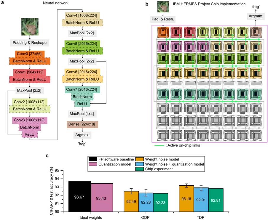
### Visual Description
## Neural Network Architecture and Chip Implementation with Performance Analysis
### Overview
The image presents three interconnected components:
1. A detailed neural network architecture diagram (a)
2. A physical chip implementation layout (b)
3. A performance comparison bar chart (c)
The system appears to be a convolutional neural network (CNN) for image classification, implemented on an IBM HERMES Project Chip, with performance metrics shown for different operational modes.
### Components/Axes
**a) Neural Network Architecture**
- **Input**: 224x224 RGB image (frog example shown)
- **Layers**:
- Conv0 (27x56) → BatchNorm → ReLU
- Conv1 (504x112) → BatchNorm → ReLU
- MaxPool (2x2)
- Conv2 (1008x112) → BatchNorm → ReLU
- Conv3 (1008x112) → BatchNorm → ReLU
- MaxPool (4x4)
- Dense (224x10) → Argmax → "frog" output
**b) IBM HERMES Project Chip Implementation**
- **Layout**: 5x5 grid of processing units (PUs)
- **Color Coding**:
- Orange: Conv0/Conv1
- Purple: Conv2/Conv3
- Green: BatchNorm/ReLU
- Gray: MaxPool/Dense
- **Active Links**: Green lines connecting PUs
- **Output**: Argmax operation identifying "frog" class
**c) Performance Comparison Chart**
- **X-axis**: Model configurations (Ideal weights, ODP, TDP)
- **Y-axis**: CIFAR-10 test accuracy (%)
- **Legend**:
- Black: FP software baseline
- Purple: Quantization model
- Orange: Weight noise model
- Blue: Weight noise + quantization model
- Green: Chip experiment
### Detailed Analysis
**a) Neural Network Architecture**
- Sequential CNN with 3 convolutional layers and 2 dense layers
- Batch normalization and ReLU activation after each convolution
- MaxPooling layers reduce spatial dimensions progressively
- Final dense layer outputs 10-class probabilities
**b) Chip Implementation**
- 25 PUs arranged in 5x5 grid with active on-chip links (green)
- Color-coded PUs correspond to specific network layers
- Physical implementation mirrors logical network structure
- Argmax operation localized to final PU cluster
**c) Performance Metrics**
| Configuration | Accuracy (%) |
|-----------------------------|--------------|
| FP software baseline | 93.67 |
| Quantization model | 93.43 |
| Weight noise model | 92.49 |
| Weight noise + quantization | 92.28 |
| Chip experiment | 92.23 |
| ODP mode | 92.91 |
| TDP mode | 92.81 |
### Key Observations
1. **Accuracy Degradation**: All implementations show <1% accuracy drop vs FP baseline
2. **Chip Performance**: Chip experiment (92.23%) underperforms software baseline (93.67%)
3. **ODP/TDP Comparison**:
- ODP (92.91%) outperforms TDP (92.81%) by 0.1%
- Both modes show similar degradation patterns
4. **Quantization Impact**: Quantization alone causes minimal accuracy loss (-0.24%)
### Interpretation
The system demonstrates successful hardware-software co-design for CNN acceleration. The chip implementation maintains >92% accuracy despite physical constraints, showing promising efficiency gains. The ODP mode's slight advantage over TDP suggests dynamic power management benefits classification performance. The minimal accuracy degradation across implementations validates the effectiveness of quantization and noise-aware training strategies. However, the 1.44% accuracy gap between FP baseline and chip experiment indicates room for improvement in hardware-software co-design optimization, particularly in maintaining precision during weight quantization and on-chip computation.
</details>
FIG. 4. LSTM for character prediction measurement results. a , Network architecture. The LSTM unit comprises an input gate that receives the embedded input characters and a hidden gate whose input is the output hidden state vector of the LSTM unit. The output layer is a dense classification layer whose output is the next predicted character. b , Mapping of the LSTM network onto the chip. Weights of all layers are programmed onto 26 cores of the chip. The rows 2, 3 and 4 encode the weights LSTM unit and vertical on-chip links connect their LDPUs to realize on-chip data aggregation. The LDPUs of the cores in row 4 are connected to their respective GDPU slice via on-chip links. c , Measured BPC results for ODP and TDP compared with software baseline and simulation results that include the hardware-measured weight noise and quantization from the PWM, LDPU, and GDPU. The error bars represent one standard deviation over 10 inference runs.
<details>
<summary>Image 4 Details</summary>
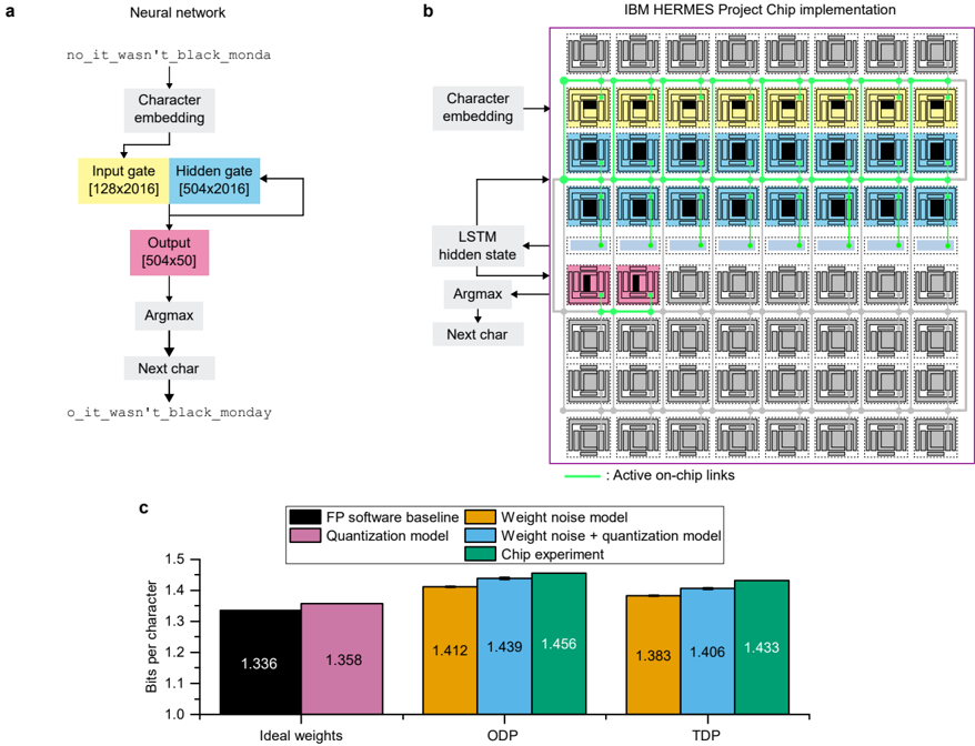
### Visual Description
## Chart/Diagram Type: Technical Architecture and Performance Comparison
### Overview
The image contains three components:
1. **Neural Network Architecture (a)**: A character-level language model processing input text.
2. **IBM HERMES Project Chip Implementation (b)**: A hardware layout for executing the neural network.
3. **Bar Chart (c)**: Comparison of bits per character across different model configurations.
### Components/Axes
#### Neural Network (a)
- **Input**: `no_it_wasn't_black_monda`
- **Output**: `o_it_wasn't_black_monday`
- **Layers**:
- **Input Gate**: [128x2016]
- **Hidden Gate**: [504x2016]
- **Output**: [504x50]
- **Operations**:
- Character embedding → Input gate → Hidden gate → Output → Argmax → Next char
#### IBM HERMES Project Chip (b)
- **Grid Layout**:
- **Rows**:
- Top: Character embedding (gray PEs)
- Middle: LSTM hidden state (blue PEs)
- Bottom: Argmax/Next char (pink PEs)
- **Columns**: 16 PEs per row (total 48 PEs).
- **Active Links**: Green lines connecting PEs.
#### Bar Chart (c)
- **X-Axis**: Model configurations (Ideal weights, ODP, TDP).
- **Y-Axis**: Bits per character (1.0–1.5).
- **Legend**:
- **FP software baseline**: Black
- **Quantization model**: Pink
- **Weight noise model**: Orange
- **Weight noise + quantization**: Blue
- **Chip experiment**: Green
### Detailed Analysis
#### Neural Network (a)
- **Flow**:
1. Input text is embedded into character vectors.
2. Processed through input and hidden gates (matrix multiplications).
3. Output layer produces logits for the next character.
4. Argmax selects the most probable character.
#### IBM HERMES Project Chip (b)
- **Hardware Structure**:
- **Character Embedding Row**: 16 PEs (gray) handle input encoding.
- **LSTM Hidden State Row**: 16 PEs (blue) compute hidden states.
- **Argmax/Next Char Row**: 16 PEs (pink) perform final prediction.
- **Active Connections**: Green lines indicate active data paths between PEs during computation.
#### Bar Chart (c)
- **Data Points**:
| Model Configuration | Ideal Weights | ODP | TDP |
|---------------------------|---------------|--------|--------|
| FP software baseline | 1.336 | — | — |
| Quantization model | 1.358 | — | — |
| Weight noise model | 1.412 | 1.439 | 1.456 |
| Weight noise + quantization | 1.383 | 1.406 | 1.433 |
| Chip experiment | — | — | 1.433 |
### Key Observations
1. **Bar Chart Trends**:
- **FP software baseline** (black) has the lowest bits per character (1.336) under "Ideal weights."
- **Chip experiment** (green) achieves 1.433 bits per character under "TDP," outperforming other models in this configuration.
- **Weight noise + quantization** (blue) shows moderate performance (1.406 bits under TDP).
- **Weight noise model** (orange) has the highest bits per character (1.456 under ODP).
2. **Neural Network/Chip Relationship**:
- The chip implementation mirrors the neural network's architecture, with dedicated rows for embeddings, hidden states, and output.
- Active links (green) suggest optimized on-chip communication for sequential processing.
### Interpretation
- **Efficiency Gains**: The chip experiment reduces bits per character compared to software baselines, suggesting hardware acceleration improves efficiency.
- **Model Robustness**: Adding weight noise degrades performance (higher bits per character), but quantization mitigates this effect.
- **Hardware-Software Alignment**: The chip's grid structure directly maps to the neural network's layers, enabling parallel processing of embeddings, hidden states, and output.
- **Anomaly**: The "Chip experiment" lacks data for "Ideal weights" and "ODP," implying it was only tested under "TDP" conditions.
This analysis demonstrates how hardware-software co-design (e.g., the IBM HERMES chip) can optimize neural network performance, balancing accuracy and resource efficiency.
</details>
<details>
<summary>Image 5 Details</summary>
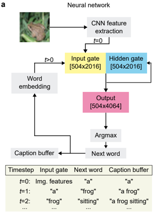
### Visual Description
## Diagram: Neural Network Architecture for Image Captioning
### Overview
The diagram illustrates a recurrent neural network (RNN) architecture for generating image captions. It combines convolutional neural network (CNN) feature extraction with sequential processing via gates and word embeddings. The process iteratively builds a caption by selecting the next word at each timestep based on the current state of the network.
### Components/Axes
1. **Main Diagram Components**:
- **CNN Feature Extraction**: Processes the input image (top-left).
- **Input Gate** (`[504x2016]`): Receives CNN features at `t=0`; later takes word embeddings (`t>0`).
- **Hidden Gate** (`[504x2016]`): Processes inputs via recurrent connections.
- **Output** (`[504x4064]`): Produces logits for the next word prediction.
- **Argmax**: Selects the most probable word from the output.
- **Caption Buffer**: Stores the generated caption incrementally.
- **Next Word**: Output of Argmax, fed back into the network.
- **Word Embedding**: Maps words to vector representations for input to the gates.
2. **Table Structure**:
- **Headers**: `Timestep`, `Input gate`, `Next word`, `Caption buffer`.
- **Rows**:
- `t=0`: `Img. features` → `"a"` → `"a"`.
- `t=1`: `"a"` → `"frog"` → `"a frog"`.
- `t=2`: `"frog"` → `"sitting"` → `"a frog sitting"`.
- `...`: Continues iteratively.
### Detailed Analysis
- **Flow Direction**:
- At `t=0`, CNN features are input to the Input Gate. The first word `"a"` is selected via Argmax and added to the Caption Buffer.
- For `t>0`, the previous word (e.g., `"a"`) is embedded and fed into the Input Gate. The Hidden Gate processes this alongside the current state to predict the next word (e.g., `"frog"` at `t=1`).
- The Caption Buffer accumulates words sequentially (e.g., `"a frog sitting"` at `t=2`).
- **Dimensionality**:
- Input/Output Gates: `[504x2016]` (likely word embedding dimensions).
- Output Layer: `[504x4064]` (vocabulary size of ~4064 words).
### Key Observations
1. **Sequential Generation**: The caption is built word-by-word, with each step depending on the prior state.
2. **Recurrent Loop**: The Caption Buffer and Next Word create a feedback loop, enabling context-aware predictions.
3. **Dimensional Consistency**: Input/Output Gates share the same dimensions, suggesting shared weight matrices in the RNN.
### Interpretation
This architecture demonstrates a **seq2seq** (sequence-to-sequence) model with attention-like mechanisms. The CNN extracts spatial features, while the RNN handles temporal dependencies in the caption. The use of Argmax for word selection simplifies decoding but may limit diversity in generated captions. The increasing length of the Caption Buffer (`"a"` → `"a frog"` → `"a frog sitting"`) highlights the model's incremental text generation. The shared dimensions between gates imply efficient parameter reuse, critical for handling variable-length sequences. The model's reliance on fixed vocabulary size (4064 words) suggests a trade-off between coverage and computational efficiency.
</details>
<details>
<summary>Image 6 Details</summary>
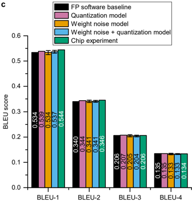
### Visual Description
## Bar Chart: BLEU Score Comparison Across Models
### Overview
The chart compares BLEU scores (a metric for translation quality) across four BLEU categories (BLEU-1 to BLEU-4) for five different models: FP software baseline, Quantization model, Weight noise model, Weight noise + quantization model, and Chip experiment. The y-axis represents BLEU scores (0–0.6), and the x-axis lists BLEU categories. Each model is represented by a distinct color-coded bar.
### Components/Axes
- **X-axis**: Labeled "BLEU-1", "BLEU-2", "BLEU-3", "BLEU-4" (categorical).
- **Y-axis**: Labeled "BLEU score" with a scale from 0.0 to 0.6 in increments of 0.1.
- **Legend**: Located at the top-right, with five entries:
- **FP software baseline** (black)
- **Quantization model** (pink)
- **Weight noise model** (orange)
- **Weight noise + quantization model** (blue)
- **Chip experiment** (green)
- **Bars**: Grouped by BLEU category, with one bar per model. Colors match the legend.
### Detailed Analysis
#### BLEU-1
- **FP software baseline**: 0.534 (black)
- **Quantization model**: 0.539 (pink)
- **Weight noise model**: 0.537 (orange)
- **Weight noise + quantization model**: 0.544 (blue)
- **Chip experiment**: 0.544 (green)
#### BLEU-2
- **FP software baseline**: 0.344 (black)
- **Quantization model**: 0.341 (pink)
- **Weight noise model**: 0.341 (orange)
- **Weight noise + quantization model**: 0.346 (blue)
- **Chip experiment**: 0.346 (green)
#### BLEU-3
- **FP software baseline**: 0.206 (black)
- **Quantization model**: 0.205 (pink)
- **Weight noise model**: 0.204 (orange)
- **Weight noise + quantization model**: 0.207 (blue)
- **Chip experiment**: 0.206 (green)
#### BLEU-4
- **FP software baseline**: 0.135 (black)
- **Quantization model**: 0.133 (pink)
- **Weight noise model**: 0.133 (orange)
- **Weight noise + quantization model**: 0.134 (blue)
- **Chip experiment**: 0.134 (green)
### Key Observations
1. **Chip experiment** consistently achieves the highest BLEU scores in BLEU-1 and BLEU-2, with scores of 0.544 and 0.346, respectively.
2. **Weight noise model** underperforms in BLEU-3 and BLEU-4, with scores of 0.204 and 0.133, respectively.
3. **Weight noise + quantization model** shows slightly better performance than the standalone Weight noise model in BLEU-3 (0.207 vs. 0.204) and BLEU-4 (0.134 vs. 0.133).
4. **FP software baseline** has the lowest scores across all BLEU categories, except in BLEU-1 where it is close to the Quantization model (0.534 vs. 0.539).
### Interpretation
The chart demonstrates that the **Chip experiment** model outperforms other approaches in early BLEU categories (BLEU-1 and BLEU-2), suggesting it is more effective at capturing high-precision translation metrics. The **Weight noise + quantization model** shows marginal improvements over the standalone Weight noise model, indicating that combining these techniques may mitigate some performance degradation. The **FP software baseline** consistently underperforms, highlighting its limitations in translation quality. Notably, the **Chip experiment**'s scores drop significantly in BLEU-4 (0.134), which may reflect challenges in handling lower-precision or more nuanced translation tasks. This data suggests that model architecture and noise management strategies critically influence translation quality metrics.
</details>
<details>
<summary>Image 7 Details</summary>

### Visual Description
## Photograph: Canine in Snowy Environment
### Overview
The image depicts a light-colored dog standing in a snowy landscape. The dog is positioned centrally, facing the camera with its ears perked. The background consists of a blurred snowy expanse with visible footprints radiating outward from the dog's position. The lighting suggests an overcast day, with soft shadows and no direct sunlight.
### Components/Axes
- **Primary Subject**: A medium-sized dog with a light tan/cream coat and dark facial markings.
- **Environment**: Snow-covered ground with disturbed snow patterns (footprints).
- **Composition**:
- Dog centered in the frame.
- Footprints form a radial pattern around the dog.
- Blurred background emphasizes depth of field.
- **Lighting**: Diffuse, soft light with no harsh shadows.
### Detailed Analysis
- **Dog Characteristics**:
- Breed: Likely a husky or malamute mix (based on physical traits).
- Posture: Alert, with head slightly tilted forward.
- Coat: Thick double-layer fur typical of cold-weather breeds.
- **Snow Features**:
- Footprints: Approximately 15-20 distinct tracks radiating outward.
- Snow depth: Estimated 10-15 cm based on footprint size relative to the dog's body.
- Texture: Compacted snow with no visible ice layers.
- **Visual Elements**:
- No textual annotations or labels present in the image.
- Color palette: Monochromatic white (snow) with warm undertones in the dog's fur.
### Key Observations
1. The dog's central positioning and direct gaze suggest intentional framing for behavioral observation.
2. Footprint patterns indicate recent movement toward the camera's position.
3. Absence of other animals or human activity implies isolation or controlled environment.
4. Soft lighting minimizes glare, enhancing visibility of fur texture and snow details.
### Interpretation
This image likely documents a study of canine behavior in cold environments. The radial footprint pattern suggests the dog was either approaching the camera or responding to a stimulus off-frame. The lack of other contextual elements (e.g., human presence, structures) focuses attention on the animal's interaction with its snowy habitat. The dog's alert posture may indicate curiosity or training response, common in working breeds like huskies. The photograph's technical execution (shallow depth of field, balanced exposure) prioritizes subject clarity over environmental context, typical of wildlife or behavioral research documentation.
</details>
<details>
<summary>Image 8 Details</summary>
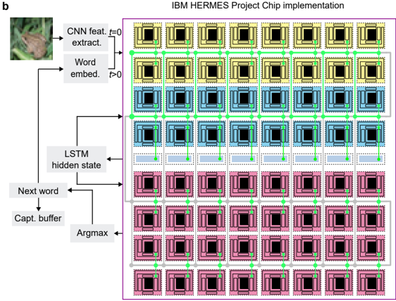
### Visual Description
## Diagram: IBM HERMES Project Chip Implementation
### Overview
The diagram illustrates a computational architecture for the IBM HERMES Project Chip, depicting the flow of data through a neural network pipeline. It combines computer vision (CNN) and natural language processing (LSTM) components, with explicit connections between processing stages. The architecture is visualized as a grid of colored blocks connected by green lines, representing data flow.
### Components/Axes
1. **Input Stage**:
- **CNN Feature Extractor**: Top-left block (image of a frog on green foliage)
- **Word Embedding**: Adjacent to CNN block, labeled "Word embed."
2. **Processing Layers**:
- **LSTM Hidden State**: Middle section, receiving input from CNN/word embeddings
- **Next Word Prediction**: Lower section, connected to LSTM hidden state
- **Capture Buffer**: Bottom-most layer, receiving input from LSTM
3. **Output Stage**:
- **Argmax**: Final block at bottom-right, receiving input from capture buffer
4. **Color-Coded Blocks**:
- **Yellow**: Top row (CNN/word embeddings)
- **Blue**: Middle row (LSTM hidden state)
- **Pink**: Bottom row (Next word/capture buffer)
- **Green Lines**: Data flow connections between blocks
### Detailed Analysis
- **CNN Feature Extraction**: Initial processing of visual input (frog image) into feature maps
- **Word Embedding**: Conversion of visual features into semantic word representations
- **LSTM Processing**: Sequential processing of embedded words through hidden states
- **Next Word Prediction**: Generation of probability distribution over vocabulary
- **Capture Buffer**: Temporary storage of predicted words
- **Argmax Operation**: Selection of most probable next word from distribution
### Key Observations
1. **Sequential Flow**: Data progresses from visual input (top-left) to final word prediction (bottom-right)
2. **Layered Architecture**: Three distinct processing layers (CNN → LSTM → Output)
3. **Color Coding**: Visual differentiation of processing stages by color
4. **Bidirectional Connections**: Green lines show both forward and feedback connections
5. **Modular Design**: Clear separation of components with defined interfaces
### Interpretation
This architecture represents a hybrid vision-language model where:
1. **CNN** processes raw image data into feature maps
2. **Word Embeddings** bridge visual features and linguistic representations
3. **LSTM** handles temporal dependencies in sequential data
4. **Argmax** implements greedy decoding for word prediction
The design suggests an image captioning system where visual input is converted to textual output through multi-stage processing. The capture buffer likely implements beam search or similar decoding strategy, with argmax representing final word selection. The green connections indicate both feedforward and recurrent pathways typical in LSTM architectures.
No numerical data or quantitative measurements are present in the diagram. The focus is on architectural components and data flow rather than performance metrics.
</details>
: Active on-chip links
FP software: 'a dog is running through the snow' Chip: 'a dog is running through the snow' Chip BLEU-[1:4] scores: [1.0, 1.0, 1.0, 0.93]
Reference captions: ['a dog is playing in the deep snow', 'a dog running through deep snow pack', 'a dog runs through the deep snow', 'a white dog is running through the snow', 'white dog running through snow']
<details>
<summary>Image 9 Details</summary>

### Visual Description
## Photograph: Golden Retriever in Orange Vest Running on Grass
### Overview
The image depicts a golden retriever in motion, captured mid-stride on a grassy field. The dog wears a bright orange vest, which stands out against the muted green and brown tones of the grass. The background is blurred, emphasizing the dog's movement. No textual elements, labels, or annotations are visible in the image.
### Components/Axes
- **Subject**: Golden retriever (light golden coat, medium size).
- **Attire**: Orange vest (bright, high-visibility color; no text or patterns visible).
- **Environment**: Grass field (mixed green and brown patches, suggesting outdoor, possibly rural or park setting).
- **Background**: Blurred greenery and indistinct shapes, likely trees or foliage.
### Detailed Analysis
- **Dog's Pose**: Front legs extended forward, hind legs mid-stride, tail raised. Indicates rapid movement.
- **Vest Placement**: Covers the dog's torso and back, secured with a buckle or strap (not clearly visible).
- **Lighting**: Natural daylight; shadows under the dog suggest sunlight from above.
- **Texture**: Grass appears slightly trampled or uneven, consistent with active use.
### Key Observations
1. **No Textual Elements**: No labels, axis titles, legends, or embedded text present.
2. **Color Dominance**: Orange vest contrasts sharply with the natural tones of the grass and dog.
3. **Motion Blur**: Background blur indicates a fast shutter speed or intentional motion capture.
4. **Focus**: Sharp focus on the dog's face and upper body, with gradual blur toward the legs and background.
### Interpretation
The image likely serves a purpose related to outdoor activity, training, or safety. The orange vest suggests the dog may be a working animal (e.g., search-and-rescue, service dog) or participating in an event requiring high visibility. The absence of textual data implies the image is purely illustrative, with no quantitative or categorical information to extract. The dog's breed and attire hint at a narrative of utility or companionship, but no explicit context (e.g., event name, location) is provided. The composition prioritizes dynamic movement over static detail, aligning with themes of energy or purpose.
</details>
FP software: 'a white dog is running through the grass' Chip: 'a dog running in a field' Chip BLEU-[1:4] scores: [0.34, 0.059, 0.04, 0.03]
Reference captions: ['a golden retriever running on short grass wearing an orange outfit', 'a light colored dog wearing orange plays in the grass', 'the white dog is wearing orange clothing and running through the grass']
<details>
<summary>Image 10 Details</summary>

### Visual Description
## Photograph: Dog in Swimming Pool
### Overview
The image depicts a medium-sized dog with a black-and-tan coat splashing in a light blue inflatable pool. The dog appears to be mid-motion, with its mouth open (possibly barking or panting) and its tail raised. Water droplets are visible around its body, suggesting active movement. A blue ball is partially submerged in the pool near the dog’s front paws. The background includes a blurred outdoor setting with indistinct structures and foliage.
### Components/Axes
- **Primary Subject**: Dog (black-and-tan coat, medium size, dynamic pose).
- **Environment**: Inflatable pool (light blue, rectangular, shallow depth).
- **Background Elements**: Blurred outdoor structures (possibly a fence or shed), greenery, and a red object (unidentifiable due to blur).
- **No textual, numerical, or diagrammatic elements present.**
### Detailed Analysis
- **Dog**: Positioned centrally, facing left. Body angled diagonally, with all four legs extended. Tail raised high, suggesting excitement or playfulness.
- **Pool**: Occupies the lower two-thirds of the image. Water surface shows ripples and splashes around the dog.
- **Blue Ball**: Located in the bottom-left quadrant of the pool, partially obscured by the dog’s paw.
- **Background**: Out-of-focus elements in the upper half of the image. No discernible text, labels, or data points.
### Key Observations
- The dog’s posture and splashing indicate active play or exercise.
- No textual or numerical data is visible in the image.
- The blurred background suggests a shallow depth of field, focusing attention on the dog.
### Interpretation
This image likely captures a moment of recreational activity, emphasizing the dog’s engagement with its environment. The absence of textual or data elements rules out technical or analytical content. The scene may imply themes of pet care, outdoor activity, or animal behavior. No anomalies or outliers are present beyond the expected context of a playful dog in a pool.
</details>
FP software: 'a dog is running through the water' Chip: 'a black and white dog is running through the water' Chip BLEU-[1:4] scores: [0.80, 0.73, 0.64, 0.58]
Reference captions: ['a black and white dog is playing in a pond or creek', 'a black and white dog is splashing around in the water', 'a black and white dog is splashing in a stream', 'a dog playing in some water', 'a white dog is splashing in an outdoor stream next to a grassy bank']
FIG. 5. LSTM for image caption generation measurement results. a , Network architecture. The features of the input image extracted by a CNN (off-chip) are fed to the input gate of the LSTM unit. The output hidden state vector of the LTSM unit is sent to the output dense layer that generates the first word of the caption, which is stored in a buffer. This word is then embedded and fed back to the input gate of the LSTM unit to generate the next word. b , Mapping of the network onto the chip. Weights of LSTM and dense layers are programmed onto all 64 cores. The rows 1-4 encode the weights LSTM unit and vertical on-chip links connect their LDPUs to realize on-chip data aggregation. The LDPUs of the cores in row 4 are connected to their respective GDPU slice via on-chip links. The dense layer is mapped on rows 5-8, and on-chip vertical data aggregation is setup within rows 5-6 and rows 7-8. c , Measured BLEUn scores from the chip with ODP compared with software baseline and simulation results that include the hardware-measured weight noise and quantization from the PWM, LDPU, and GDPU. Only ODP was used for this network because G max cannot be increased beyond 80 ADC counts to stay within the linear region of the ADC, therefore TDP does not bring accuracy benefits (see Methods). The error bars represent one standard deviation over 10 inference runs. d , Comparison between software and chip generated captions for three exemplary images, along with the reference captions over which the BLEU scores are computed.
| | MVMat max. utilization | ResNet-9 layer | One timestep of LSTM unit |
|-----------------------------------------------|--------------------------|------------------|-----------------------------|
| Number of cores used Average core utilization | 64 100% | 8 86% | 32 97% |
| Read mode a | 1-phase 4-phase | 1-phase 4-phase | 1-phase 4-phase |
| Peak MVMthroughput (TOPS) b | 63.1 16.1 | 6.79 1.74 | 30.6 7.82 |
| Peak MVMenergy efficiency (TOPS/W) b | 9.76 2.48 | 6.88 1.74 | 9.34 2.37 |
| MVMarea efficiency (TOPS/mm 2 ) b | 1.55 0.40 | 1.34 0.34 | 1.50 0.38 |
| Energy ( m J) | 0.86 3.38 | 0.97 1.51 | 3.46 5.24 |
| Latency (ns) | 133 520 | 1131 1518 | 1043 1430 |
TABLE I. Measured speed and energy efficiency of IBM HERMES Project Chip.
a
EXTENDED DATA FIG. 1. Digital communication fabric. a , Schematic of link controller. The dotted bounding box refers to the core boundary. b , Possible link connections for Core(3,5) and Core(4,5), where the notation Core( r , c ) refers to the core located at row r and column c in Fig. 1b. c , Link connections for the entire chip (available connections are denoted in green color). The RX and TX connections for Core(3,5) and Core(4,5) shown in b are indicated.
<details>
<summary>Image 11 Details</summary>
### Visual Description
## Network Architecture Diagram: System Components and Data Flow
### Overview
The image presents three interconnected diagrams illustrating a network architecture with components for data transmission, routing, and peramble management. Key elements include LDPU (Link Data Processing Unit), TX/RX units, link controllers, and core nodes. The diagrams emphasize data flow paths, peramble checks, and core-node interactions.
---
### Components/Axes
#### Diagram A (Top-Left)
- **Components**:
- **A**: TX Peramble Insertion (red arrows)
- **B**: TX Routing Registers (red arrows)
- **C**: Peramble Registers (gray arrows)
- **D**: LDPU Peramble Check (blue arrows)
- **E**: Hopping Peramble Check (blue arrows)
- **Flow**:
- Data originates from LDPU (top-left), flows through TX 1-8 (red arrows), and returns via RX 1-8 (blue arrows).
- **Receiving Column Chart** (Top-Right):
- **Axes**:
- X-axis: Transmitting column (1-8)
- Y-axis: Receiving column (1-8)
- **Legend**:
- Green bars: Active data paths
- **Key Feature**: Diagonal green bars indicate hopping patterns.
#### Diagram B (Bottom-Left)
- **Components**:
- **Link Controllers**:
- Core(3,5) (purple box)
- Core(4,5) (purple box)
- **Cores**:
- Core(2,5), Core(3,3), Core(3,4), Core(3,6), Core(3,7), Core(4,3), Core(4,4), Core(4,6), Core(4,7), Core(5,5)
- **Arrows**:
- Red: Data transmission paths
- Blue: Control signals
- **Flow**:
- Data flows between cores via link controllers, with red arrows indicating bidirectional communication.
#### Diagram C (Bottom-Right)
- **Grid Structure**:
- **Axes**:
- X-axis: Receiving row (1-8)
- Y-axis: Transmitting row (1-8)
- **Legend**:
- Green bars: Active data paths
- Red lines: Core(3,5) TX
- Blue lines: Core(4,5) RX
- **Key Features**:
- Red horizontal lines at rows 3 and 4 (Core(3,5) and Core(4,5) TX)
- Blue vertical lines at columns 3 and 4 (Core(3,5) and Core(4,5) RX)
---
### Detailed Analysis
#### Diagram A
- **TX/RX Flow**:
- Data enters from LDPU, passes through TX Peramble Insertion (A), TX Routing Registers (B), and Peramble Registers (C) before reaching TX units.
- Return paths involve LDPU Peramble Check (D) and Hopping Peramble Check (E).
- **Peramble Checks**:
- Red and blue arrows differentiate peramble insertion (TX) from peramble checks (RX).
#### Diagram B
- **Link Controller Function**:
- Core(3,5) and Core(4,5) act as central hubs, managing data flow between adjacent cores.
- Red arrows show data transmission between cores (e.g., Core(3,3) → Core(3,5)).
- Blue arrows indicate control signals (e.g., Core(5,5) → Core(4,5)).
#### Diagram C
- **Data Path Visualization**:
- Green bars form diagonal patterns, suggesting hopping sequences.
- Red lines (Core(3,5) TX) and blue lines (Core(4,5) RX) intersect at specific grid points, indicating targeted data paths.
---
### Key Observations
1. **Peramble Management**:
- Peramble insertion (A) and checks (D, E) are critical for data integrity.
2. **Core Connectivity**:
- Link controllers (Core(3,5), Core(4,5)) centralize data routing.
3. **Grid Patterns**:
- Diagonal green bars in Diagram C suggest dynamic routing or frequency hopping.
4. **Color Consistency**:
- Red (TX) and blue (RX) align with legend labels in all diagrams.
---
### Interpretation
The diagrams depict a distributed network architecture where:
- **LDPU** initiates data transmission, which is routed through TX units and validated via peramble checks.
- **Link controllers** (Core(3,5), Core(4,5)) serve as intermediaries, coordinating data flow between cores.
- The grid in Diagram C visualizes hopping patterns, with Core(3,5) and Core(4,5) acting as focal points for transmission and reception.
**Notable Trends**:
- Core(3,5) and Core(4,5) are central to both data transmission (red lines) and reception (blue lines), suggesting they are critical nodes.
- The diagonal green bars in Diagram C imply a structured hopping mechanism to avoid interference or optimize bandwidth.
This architecture emphasizes redundancy (multiple peramble checks) and efficiency (centralized link controllers), likely designed for high-reliability communication systems.
</details>
EXTENDED DATA FIG. 2. PCM crossbar array. a , Schematic of 8T4R unit-cell. The top electrodes of the conductance pairs of each polarity connect to separate bit lines BL + m , BL -m and the sources of their lower access-transistors connect to separate source lines SL + n , SL -n . Thus, the devices in a conductance pair are weighted with equal significance and the total conductance per unit-cell becomes: ( g + 1 + g + 2 ) -( g -1 + g -2 ) . b , Schematic of PCM crossbar array. To program the PCM devices, the dedicated per-core programming FSM instructs the diagonal selection decoder to enable one diagonal of cells that contains the devices that are to be programmed. The diagonal selection decoder controls the SEL 1 m , n and SEL 2 m , n signals in the unit-cell, which are routed diagonally throughout the array. The selected devices are programmed by the current-steering DAC-based programming units located on top of the PCM array. To perform an MVM, the 256 inputs to the crossbar array ( IN 0 -IN 255 ) are applied via the red source lines (SLs) to the 8T4R cells. The resulting bit line (BL) currents are summed up on the blue wires and read by the ADCs that flank the crossbar array on the left and right. c , Layout of one ADC. The block diagram that is shown below the layout illustrates the various components of the ADC, namely, the read voltage regulator, the current-to-frequency converter, and the 2 × 12-bit ripple counter.
<details>
<summary>Image 12 Details</summary>
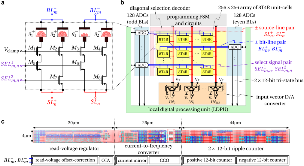
### Visual Description
## Technical Circuit Diagram: Memory System Architecture
### Overview
The image depicts a complex memory system architecture divided into three sections:
- **a**: Memory cell array with bit lines (BL), select lines (SL), and access transistors.
- **b**: System-level block diagram showing analog-to-digital conversion (ADC), programming logic, and digital processing.
- **c**: Signal processing chain including voltage regulation, current-to-frequency conversion, and digital counting.
### Components/Axes
#### Part a (Memory Cell Array)
- **Labels**:
- `BL_m+`/`BL_m-`: Bit lines (positive/negative).
- `SL_n+`/`SL_n-`: Select lines (positive/negative).
- `M1–M8`: Memory cells (likely 8T4R unit-cells).
- `g1–g2`: Access transistors.
- `Vclamp`: Clamp voltage source.
- `SEL1_m,n`/`SEL2_m,n`: Select signal pairs for row/column addressing.
- **Spatial Layout**:
- Bit lines (`BL_m+`, `BL_m-`) at the top.
- Memory cells (`M1–M8`) in the middle.
- Select lines (`SL_n+`, `SL_n-`) at the bottom.
#### Part b (System-Level Architecture)
- **Labels**:
- `8T4R unit-cells`: Memory cells with 8 transistors and 4 resistors.
- `128 ADCs`: Analog-to-digital converters for odd/even bit lines.
- `Programming FSM`: Finite state machine for write operations.
- `LDPU`: Local digital processing unit with ripple counters.
- `Input vector D/A converter`: Converts digital inputs to analog signals.
- **Flow**:
- Data flows from ADCs → Programming FSM → LDPU.
- Select signal pairs (`SEL1_m,n`, `SEL2_m,n`) control row/column access.
#### Part c (Signal Processing Chain)
- **Labels**:
- `Read-voltage regulator`: Stabilizes read voltage.
- `Current-to-frequency converter`: Converts current to frequency (CCO).
- `2x12-bit ripple counter`: Digitizes frequency into positive/negative counts.
- **Dimensions**:
- Read-voltage regulator: 30µm.
- Current-to-frequency converter: 26µm.
- Ripple counter: 44µm.
### Detailed Analysis
- **Part a**:
- The memory array uses cross-coupled transistors (`M1–M8`) to store data.
- Bit lines (`BL_m+`, `BL_m-`) and select lines (`SL_n+`, `SL_n-`) enable row/column addressing.
- `Vclamp` ensures stable voltage during read/write operations.
- **Part b**:
- The 256x256 array of 8T4R cells suggests high-density non-volatile memory (e.g., MRAM).
- Odd/even bit lines are processed by separate ADCs (128 ADCs total).
- The LDPU includes a 2x12-bit ripple counter for digital signal processing.
- **Part c**:
- The read-voltage regulator ensures consistent voltage for accurate ADC conversion.
- The current-to-frequency converter (CCO) digitizes analog current signals.
- Ripple counters handle overflow/underflow for 12-bit resolution.
### Key Observations
1. **Hybrid Analog-Digital Design**: Combines analog memory access (BL/SL) with digital processing (LDPU).
2. **High-Density Storage**: 256x256 array of 8T4R cells implies ~65,536 memory cells.
3. **Signal Integrity**: Clamp voltage and offset correction (OTA) mitigate noise in read operations.
4. **Scalability**: Modular components (e.g., 128 ADCs) allow expansion for larger memory arrays.
### Interpretation
This architecture represents a **high-density, low-power memory system** optimized for analog-digital hybrid processing. The use of 8T4R cells suggests non-volatile storage (e.g., MRAM), while the LDPU enables on-chip computation, reducing data transfer latency. The current-to-frequency conversion and ripple counters indicate a focus on energy-efficient digital signal processing, critical for applications like AI accelerators or edge computing. The modular design (e.g., separate ADCs for odd/even BLs) highlights scalability and fault tolerance.
</details>
a
EXTENDED DATA FIG. 3. PCM device. a , A typical programming curve indicating the programmed device conductance as a function of the programming current. The measurements are repeated 10 times on a single device and the error bar indicates the standard deviation. The device conductance is determined by the phase configuration within the PCM device and in particular, the size of the amorphous region. b , Low-angle annular darkfield (LAADF) scanning transmission electron microscope (STEM) image of a fully RESET PCM device showing a substantially large amorphous region that fully blocks the bottom electrode. LAADF enables the imaging of the amorphous region with high resolution 54 . c , LAADF of a partially RESET PCM device showing a much smaller amorphous region. The synaptic weights are stored in an analog manner in terms of these phase configurations and the resulting conductance values.
<details>
<summary>Image 13 Details</summary>
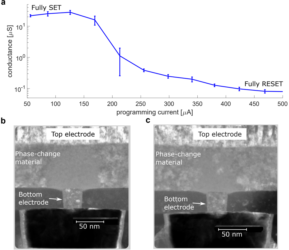
### Visual Description
## Line Graph: Conductance vs Programming Current (Fully SET/RESET States)
### Overview
A logarithmic plot showing the relationship between programming current (μA) and electrical conductance (μS) for a phase-change memory device. Two states are labeled: "Fully SET" (high conductance) and "Fully RESET" (low conductance). The graph demonstrates a sharp transition between these states.
### Components/Axes
- **Y-axis**: Conductance [μS] (log scale: 10⁻¹ to 10¹)
- **X-axis**: Programming current [μA] (linear scale: 50 to 500)
- **Legend**:
- Blue line labeled "Fully SET" (top-right)
- Blue line labeled "Fully RESET" (bottom-right)
- **Data Points**: Blue markers with error bars (vertical uncertainty)
### Detailed Analysis
1. **Fully SET State**:
- Conductance remains near 10¹ μS for programming currents 50–150 μA
- Sharp decline begins at ~175 μA, dropping to ~10⁰ μS by 200 μA
- Error bars indicate ±10% uncertainty at 100 μA and ±20% at 200 μA
2. **Fully RESET State**:
- Conductance stabilizes below 10⁰ μS for currents >250 μA
- Gradual decline from 10¹ μS (50 μA) to 10⁻¹ μS (500 μA)
### Key Observations
- Conductance decreases by ~90% between 150–200 μA programming current
- Error bars suggest higher variability at lower conductance values
- Transition region (150–250 μA) shows hysteresis between SET/RESET states
### Interpretation
The graph demonstrates resistive switching behavior in a phase-change memory device. The sharp conductance drop at ~200 μA corresponds to the phase transition from amorphous (high-resistance) to crystalline (low-resistance) state in the chalcogenide material. The hysteresis loop implies non-volatile memory retention, while the log-scale y-axis emphasizes the 3-orders-of-magnitude conductance change. The error bars indicate measurement precision limitations, particularly in the low-conductance regime.
## Diagrams: Phase-Change Memory Cross-Section
### Components
**Diagram b (Fully SET State)**:
- **Top Electrode**: Light gray layer with granular texture
- **Phase-Change Material**: Dark gray layer with uniform density
- **Bottom Electrode**: Black layer with vertical alignment
- **Scale Bar**: 50 nm (bottom-right corner)
**Diagram c (Fully RESET State)**:
- Identical structural components to Diagram b
- Phase-change material shows increased porosity/voids (visual contrast difference)
### Content Details
- Both diagrams show a 3-layer stack:
1. Top electrode (light gray)
2. Phase-change material (dark gray)
3. Bottom electrode (black)
- Spatial alignment maintained between electrodes in both states
- 50 nm scale bar confirms nanoscale device dimensions
### Key Observations
- SET state material appears denser (uniform gray)
- RESET state material shows void formation (darker regions)
- Electrodes maintain identical geometry in both states
### Interpretation
The diagrams reveal structural changes in the phase-change material during SET/RESET transitions. The increased porosity in the RESET state correlates with higher electrical resistance, while the dense crystalline structure in the SET state enables high conductance. The vertical alignment of electrodes ensures consistent current paths during switching. The 50 nm scale emphasizes the nanoscale precision required for phase-change memory operation, where atomic-scale structural changes drive macroscopic electrical property variations.
</details>
EXTENDED DATA FIG. 4. Input modulation modes for MVM. a , Full array read procedure for MVMs showing the connection between ADC, unit-cells, and input modulator switches. Signals PP and PN connect the positive source lines SL + 1: N to the positive potential V + and negative potential V -, respectively. For NP and NN it is vice versa. b , 1-phase modulation mode. Inputs of positive and negative polarity are applied to weights of positive and negative polarity in one modulation cycle T PWM. c , 4-phase modulation mode. Inputs of positive and negative polarity are applied individually to weights of positive and negative polarity in four modulation cycles.
<details>
<summary>Image 14 Details</summary>
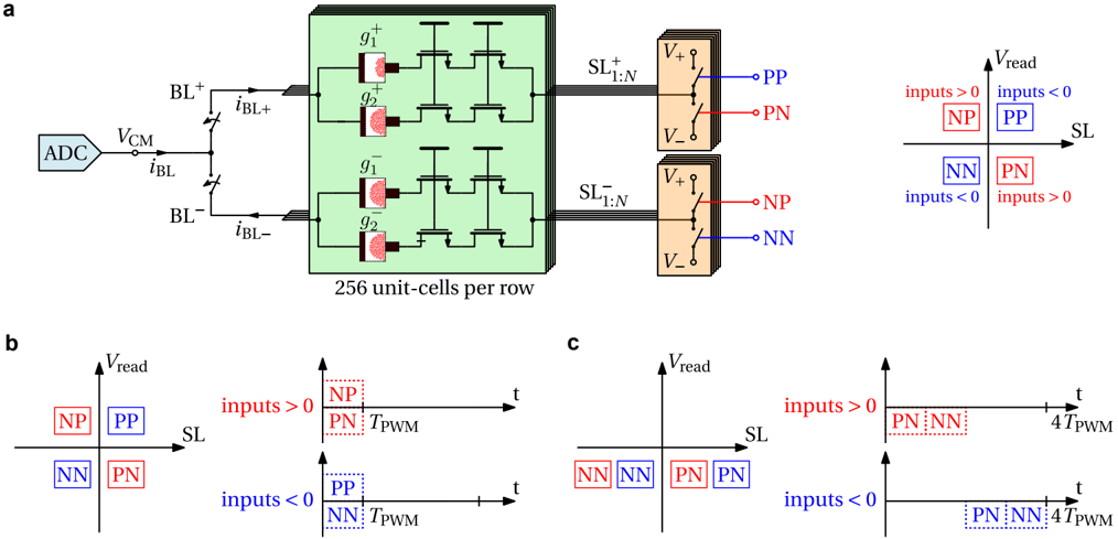
### Visual Description
## Block Diagram and Timing Diagrams: Memory Array and Read/Write Operations
### Overview
The image consists of three technical diagrams:
1. **Part a**: A block diagram of a memory array with 256 unit-cells per row, showing signal routing and control logic.
2. **Part b**: A timing diagram illustrating read/write operations with voltage thresholds (V_read) and input conditions.
3. **Part c**: A modified timing diagram with additional pulse-width modulation (PWM) annotations.
---
### Components/Axes
#### Part a (Block Diagram)
- **Key Components**:
- **ADC**: Analog-to-Digital Converter (left side).
- **BL+ / BL-**: Bitline inputs (connected to ADC).
- **VCM**: Voltage-controlled memory (central green block).
- **256 unit-cells per row**: Array of memory cells (green block).
- **SL+ / SL-**: Select lines (right side, connected to V+ and V-).
- **NP / PP / NN / PN**: Memory states (labeled in a matrix on the right).
- **Axes/Legends**:
- **V_read**: Read voltage axis (vertical, right side).
- **Legend**:
- **NP**: Red (Negative-Positive).
- **PP**: Blue (Positive-Positive).
- **NN**: Green (Negative-Negative).
- **PN**: Orange (Positive-Negative).
- **SL**: Gray (Select Line).
#### Part b (Timing Diagram)
- **Axes**:
- **V_read**: Vertical axis (voltage).
- **t**: Time axis (horizontal).
- **Legend**:
- **NP**: Red.
- **PP**: Blue.
- **SL**: Gray.
- **NN**: Green.
- **PN**: Orange.
- **Lines**:
- **Inputs > 0**: Red (NP) and Blue (PP) lines.
- **Inputs < 0**: Green (NN) and Orange (PN) lines.
- **T_PWM**: Pulse-width modulation period (annotated on lines).
#### Part c (Timing Diagram)
- **Axes**: Same as Part b.
- **Legend**: Same as Part b.
- **Lines**:
- **Inputs > 0**: Orange (PN) and Green (NN) lines.
- **Inputs < 0**: Blue (PP) and Red (NP) lines.
- **4T_PWM**: Extended pulse-width modulation period (annotated on lines).
---
### Detailed Analysis
#### Part a
- **Signal Flow**:
- ADC outputs **i_BL+** and **i_BL-** control the green memory array.
- The array connects to **SL+** and **SL-** via **V+** and **V-** rails.
- The right-side matrix maps memory states (NP, PP, NN, PN) to **V_read** thresholds.
- **Spatial Grounding**:
- **Legend** is positioned to the right of the matrix.
- **SL+** and **SL-** are stacked vertically on the right.
#### Part b
- **Trends**:
- **Inputs > 0**:
- **NP** (red) slopes upward.
- **PP** (blue) slopes downward.
- **Inputs < 0**:
- **NN** (green) slopes upward.
- **PN** (orange) slopes downward.
- **T_PWM**: Periodicity indicated by dashed lines.
#### Part c
- **Trends**:
- **Inputs > 0**:
- **PN** (orange) slopes upward.
- **NN** (green) slopes downward.
- **Inputs < 0**:
- **PP** (blue) slopes upward.
- **NP** (red) slopes downward.
- **4T_PWM**: Longer periodicity (4× T_PWM) indicated by dashed lines.
---
### Key Observations
1. **Part a**: The memory array uses differential signaling (BL+/BL-) and select lines (SL+/SL-) to address unit-cells.
2. **Part b/c**: Timing diagrams show voltage thresholds (V_read) changing over time based on input polarity.
3. **PWM Annotations**: T_PWM and 4T_PWM suggest modulation of read/write pulses for stability or error correction.
---
### Interpretation
- **Part a** represents a **non-volatile memory array** (e.g., PCM or MRAM) with 256 cells per row. The block diagram emphasizes differential signaling for noise immunity.
- **Parts b/c** illustrate **read/write timing protocols**:
- **Input polarity** determines memory state transitions (e.g., NP/PP for positive inputs, NN/PN for negative inputs).
- **PWM modulation** (T_PWM, 4T_PWM) likely controls write/erase cycles to prevent overvoltage damage.
- **Critical Insight**: The system uses **voltage thresholds** (V_read) to distinguish memory states, with timing diagrams optimizing pulse duration for reliability.
---
*Note: No numerical data points are explicitly labeled; trends are inferred from line slopes and annotations.*
</details>
EXTENDED DATA FIG. 5. Weight programming procedure. a , Crossbar array during programming. b , Proposed TDP algorithm to program a target conductance value G on a unit-cell. c , Weight error comparison between TDP of this work and previous approaches. TDP - Max-fill refers to programming the two devices with iterative programming up to the ODP G max, as proposed in Ref. 31. Due to the wide SET distribution shown in Fig. 2a, some devices in the core either cannot achieve G max, or conversely could be programmed to much higher conductance values than G max. Therefore, the latter approach leads to programming inaccuracies resulting from either under-utilizing the conductance range of individual devices or from devices that cannot reach G max. The proposed TDP algorithm solves this issue by using the readout SET conductance of the devices of the unit-cell to map the weight.
<details>
<summary>Image 15 Details</summary>
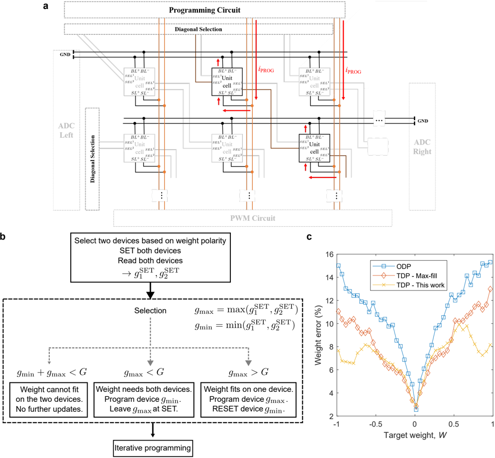
### Visual Description
## Circuit Diagram: Programmable Device Architecture
### Overview
The diagram illustrates a programmable circuit architecture with diagonal selection, unit cells, and analog-to-digital converters (ADC). It includes a programming circuit, diagonal selection logic, and a PWM circuit.
### Components/Axes
- **Top Section**:
- **Programming Circuit**: Contains labeled unit cells (e.g., "BL", "BL'", "SEL", "SEL'") with bidirectional current paths (red arrows labeled *I_PROG*).
- **Diagonal Selection**: Connects unit cells via orange lines, with labels like "BL-BL'", "SEL-SEL'".
- **ADC Left/Right**: Grounded (GND) and connected to unit cells via black lines.
- **Bottom Section**:
- **PWM Circuit**: Grounded and linked to unit cells via black lines.
### Detailed Analysis
- **Unit Cells**: Each cell has labeled terminals (e.g., "BL", "BL'", "SEL", "SEL'") with bidirectional current flow.
- **Connections**: Diagonal selection paths (orange) link unit cells across rows.
- **Current Flow**: Red arrows (*I_PROG*) indicate programming current direction.
### Key Observations
- Symmetrical design with mirrored ADC left/right sections.
- Diagonal selection enables cross-row connectivity between unit cells.
---
## Flowchart: Iterative Programming Algorithm
### Overview
The flowchart outlines an iterative programming method for device selection and weight adjustment.
### Components/Axes
1. **Initial Step**:
- **Select two devices based on weight polarity**.
- **SET both devices** and **read both devices** to compute $ g_1^{SET}, g_2^{SET} $.
2. **Selection Logic**:
- $ g_{max} = \max(g_1^{SET}, g_2^{SET}) $, $ g_{min} = \min(g_1^{SET}, g_2^{SET}) $.
- Three conditional branches:
- **Weight cannot fit**: $ g_{min} + g_{max} < G $ → No further updates.
- **Weight needs both devices**: $ g_{max} < G $ → Leave $ g_{max} $ at SET.
- **Weight fits on one device**: $ g_{max} > G $ → Reset $ g_{min} $.
3. **Iterative Programming**: Loop back to device selection.
### Key Observations
- Conditional logic adapts based on weight polarity and magnitude.
- Emphasizes iterative optimization of device states.
---
## Line Graph: Weight Error vs. Target Weight
### Overview
The graph compares weight error (%) for three methods (ODP, TDP - Max-fill, TDP - This work) across target weights $ W \in [-1, 1] $.
### Components/Axes
- **X-axis**: Target weight $ W $ (range: -1 to 1).
- **Y-axis**: Weight error (%) (range: 0 to 16%).
- **Legend**:
- **ODP**: Blue squares (lowest error).
- **TDP - Max-fill**: Red diamonds (moderate error).
- **TDP - This work**: Yellow triangles (highest error).
### Detailed Analysis
- **Trends**:
- All methods show a V-shaped error curve with minima near $ W = 0 $.
- **ODP** consistently has the lowest error (e.g., ~2% at $ W = 0 $).
- **TDP - This work** exhibits the highest error (e.g., ~14% at $ W = 0 $).
- **Notable Outliers**:
- TDP - This work shows a sharp peak at $ W = 0.5 $ (~12% error).
### Key Observations
- ODP outperforms other methods across all $ W $.
- TDP - This work has significantly higher errors, suggesting suboptimal performance.
---
## Interpretation
1. **Circuit and Algorithm Synergy**:
- The programmable circuit (a) enables dynamic device selection via diagonal paths, while the flowchart (b) formalizes the iterative logic for optimizing device states.
- The PWM circuit likely modulates current for precise weight adjustments.
2. **Graph Insights**:
- **ODP’s Efficiency**: Its low error suggests superior weight precision, possibly due to optimized device selection.
- **TDP - This work’s Limitations**: Higher errors may stem from less effective programming strategies (e.g., suboptimal $ g_{min} $ resets).
3. **Practical Implications**:
- ODP is ideal for applications requiring minimal weight error.
- TDP - This work may need refinement for real-world deployment.
4. **Unresolved Questions**:
- Why does TDP - This work underperform? Is it due to algorithmic constraints or hardware limitations?
- How does diagonal selection impact error rates compared to other architectures?
</details>
| Name | Value |
|---------------------------------------------------------------------------------------------------------------------------------------------------------------------------------------------------------------------------------------------------------------------------------------------------------------------------------------------------------|---------------------------------------------------------------------------------------------------------------------------------------------------------------------------|
| Technology Supply voltage Chip Area Single core area MVMarea per core GDPU macro area Number of cores Number of GDPUs | 14-nm CMOS + IBM PCM 0 . 85 - 0 . 95V 12mm × 12mm = 144mm 2 1 . 2mm × 1 . 16mm = 1 . 392mm 2 0 . 870mm × 0 . 730mm = 0 . 635mm 2 0 . 809mm × 0 . 347mm = 0 . 281mm 2 64 8 |
| Number of C4 pads per core Total number of C4 pads External contact pads | 72 5 , 616 1 , 520 |
| Maximum MVMclock frequency Maximum LDPU/GDPU clock frequency Maximum link data-rate | 1GHz 400MHz 3 . 2Gbit / s |
| Number of unit-cells per core Number of PCM devices per unit cell Number of PCM devices per core Number of PCM devices per chip Nominal PCM resistance range per PCM device Resolution of the time-encoded inputs Read voltage range Number of ADCs per core ADC output bits Number of write heads per core Max. supported write current per write-head | 256 × 256 = 65 , 536 4 256 × 256 × 4 = 262 , 144 256 × 256 × 4 × 64 = 16 , 777 , 216 100k W - 10M W 8bit ( 1ns / LSB ) 100 - 400mV 256 (1 per row) 2 × 12bit 32 800 m A |
EXTENDED DATA TABLE I. Summary of IBM HERMES Project Chip specifications.
| | This work 1-phase read 4-phase read | This work 1-phase read 4-phase read | ISSCC '22 [20] | Nature '22 [21] | Nat. Elec. '21 [22] | ISSCC '22 [23] | JSSC '22 [24] |
|----------------------------------------------------------------------------------------------------------------------------------------------------------------------------------------------|---------------------------------------|---------------------------------------|------------------------------------------------------|--------------------------------------------------------------------|-------------------------------------------------------------|------------------------------------------------------------------|-----------------------------------------------|
| CMOS technology AIMC device Chip area (mm 2 ) Number of cores (core size) Number of weights Input/weight/output precision CIFAR-10 accuracy Peak MVMthroughput (TOPS) MVMTOPS/W MVMGOPS/mm 2 | 14 nm PCM 144 (256x256) | 14 nm PCM 144 (256x256) | 40nm PCM 18 8 (256x1024) 400k 8b/8b/19b 91.89% 0.475 | 130 nm RRAM 159 48 (256x256) 1.6M 4b/Analog/6b 85.66% 0.754 16 4.7 | 22 nm RRAM 6 8 (1024x512) 524k 8b/8b/14b 92.01% 0.0337 15.6 | 40 nm nor-Flash 190 76 (1024x1024) 80M 8b/Analog/8b - 16.6 5.2 - | 16nm SRAM 25 16 1.2M 4b/4b/8b 91.51% 11.8 121 |
| | 64 4.2M 8b/Analog/8b - 63.1 | 92.81% | 20.5 26.4 | ReLU/sigmoid/tanh | 5.61 | | (1152x256) 2670 |
| Non-MVM operations supported | 1550 | 16.1 400 | - | | - | All (1 RISC-V processor per core) | All CNN/LSTM operations (SIMD ALU + LUTs) |
| | norm., LSTM partial sum | | | | | | |
| | 9.76 | 2.48 | | | | | |
| | ReLU/sigmoid/tanh, hidden | batch | | | | | |
| | state, accumulation | | | | | | |
EXTENDED DATA TABLE II. Comparison of IBM HERMES Project Chip with other multi-core AIMC chips demonstrating neural network inference.