# Valley-dependent transport through graphene quantum dots due to proximity-induced, staggered spin-orbit couplings
**Authors**: A. Belayadi, P. Vasilopoulos, N. Sandler
> abelayadi@usthb.dzDept. of Theoretical Physics, University of Science and Technology Houari Boumediene, Bab-Ezzouar 16111, Algeria.École Supérieure des Sciences de l’Aliment et Industries Alimentaires, ESSAIA, El Harrach 16200, Algeria.
> p.vasilopoulos@concordia.caDept. of Physics, Concordia University, 7141 Sherbrooke Ouest, Montréal, Québec H4B 1R6, Canada
> sandler@ohio.eduDept. of Physics and Astronomy, Ohio University and Nanoscale Quantum Phenomena Institute, Athens, Ohio, USA.
Abstract
We study a system composed of graphene decorated with an array of islands with $C_{3v}$ symmetry that induce quantum dot (IQD) regions via proximity effects and gives rise to several spin-orbit couplings (SOCs). We evaluate transport properties for an array of IQDs and analyze the conditions for realizing isolated valley conductances and valley-state localization. The resulting transmission shows a square-type behavior with wide gaps that can be tuned by adjusting the strength of the staggered intrinsic SOCs. Realistic proximity effects are characterized by weak SOC strengths, and the analysis of our results in this regime shows that the Rashba coupling is the important interaction controlling valley properties. As a consequence, a top gate voltage can be used to tune the valley polarization and switch the valley scattering for positive or negative incident energies. A proper choice of SOC strengths leads to higher localization of valley states around the linear array of IQDs. These systems can be implemented in heterostructures composed of graphene and semiconducting transition-metal dichalcogenides (TMDs) such as MoSe 2, WSe 2, MoS 2, or WS 2. In these setups, the magnitudes of induced SOCs depend on the twist angle, and due to broken valley degeneracy, valley polarized currents at the edges can be generated in a controllable manner as well as localized valley states. Our findings suggest an alternative approach for producing valley-polarized currents and propose a corresponding mechanism for valley-dependent electron optics and optoelectronic devices.
I introduction
The study of valleytronic materials is of significant importance in the area of information processing and encoding [1, 2, 3] due to the alternative degree of freedom furnished by the carrier’s valley momentum in addition to the conventionally used charge and/or spin properties.
The benchmark material is a two-dimensional (2D) graphene-based structure with Dirac cones at ${\bf K_{1}=-K}$ and ${\bf K_{2}=+K}$ valleys, proposed as a strong candidate for future valley-driven computing devices through the manipulation of valley currents [4, 5, 6], i.e., by applying external voltages. However, the lack of external probes or contacts that can select individual valley currents as ferromagnetic contacts separate spins polarized currents in spintronic devices [7, 8, 9], remains a primal obstacle to encoding and information processing through the valley index.
In addition to transport, the material’s optoelectronic properties are also used to access the valley degree of freedom [10, 11, 12, 13]. Several strategies have used the optical response to control, detect, and monitor valley polarization [14, 15, 16, 17]. Generally, a combination of gates voltages -implemented via scanning tunneling microscopy- and suitable substrate magnetic materials bring out the mechanism that tunes the desired electronic, spintronic, and valleytronic properties [18, 19, 20, 21] as proposed and later demonstrated by polarization-resolved photoluminescence experiments [10, 22, 13, 23, 24].
An alternative approach to induce valley separation involves exploiting confined geometries. Quantum dots (QDs) can produce valley-filtered currents and are important ingredients in modern nanotechnology devices. Typically, confined geometries that induce valley separation are obtained via a wide variety of methods that include electrostatic confinement produced by a scanning tunneling microscopy tip [20], strain fields [25], bilayer graphene structures with spatially varying broken sublattice symmetry [26] and isolated regions defined by local broken sublattice symmetry [23]. In all these setups, valley separation is achieved because of the effects of external fields or due to substrate properties that are extremely difficult to design and control with sufficient precision. As a consequence, the potential of these geometries to induce selective valley filtering and confinement in a controllable manner and without external fields remains untapped. To address this issue, we investigate the properties of a proposed heterostructure that exploits proximity effects and periodic spin-orbit interactions.
Ideally, the most efficient way to induce uniform and large staggered spin-orbit couplings (SOC)s on graphene is via proximity to appropriate substrates that break the sublattice symmetry, thus allowing for a clear distinction of the two pseudospins. Recently, the role of SOCs in valley separation has been addressed in several works, such as graphene deposited on top of hexagonal boron nitride [27] and graphene/TMD heterostructures [28, 29]. These setups possess staggered onsite potentials that give rise to various SOCs via different mechanisms [23]. Interestingly, not all types of SOCs will render valley separation as shown by the sublattice independent intrinsic spin-orbit coupling (ISOC) in the Kane and Mele model [30], or the Rashba SOC (RSOC) that appears in the presence of external fields. However, other appropriately engineered interactions can break the sublattice symmetry, rendering two main effects that we refer to as (1) the rise of a staggered potential with a concomitant gap opening and (2) the emergence of an ISOC in a staggered form that is sublattice dependent (i.e., sublattice-resolved SOC). In this last case, the spin-valley transport is due to the emergence of a valley-Zeeman type of coupling, defined by the ISOC sign change between sublattices [31, 28, 32]. This valley Zeeman effect is of great interest because it induces a giant spin lifetime anisotropy in proximitized graphene [33]. Furthermore, Frank et ${\it al}$ [34] showed that in narrow-width cells of zigzag-terminated graphene with a staggered ISOC, pseudo-helical and valley-centered states (without topological protection) are localized along the edges. These results are consistent with the bulk system’s topological invariant $Z_{2}=0$ .
In this work, we propose a heterostructure composed of graphene and TMD islands that combines the effects of confinement and SOCs in a controllable manner. The model is inspired by recent experiments reported in Ref. 51, with graphene deposited on top of a TMD island that induces a local region with various SOCs, i.e., an induced quantum dot (IDQ). Our proposal generalizes the experimental setup to a periodic array of islands placed below or deposited on the graphene membrane. The TMD islands preserve the underlying $C_{3v}$ symmetry of graphene and introduce SOCs in the electron dynamics via the proximity effect. We analyze the conditions for selective valley state confinement and the generation of valley currents under applied voltages for a generic model that is later applied to specific material combinations.
The paper is organized as follows. In Sec. II, we briefly present the model for a system composed of a linear array of induced quantum dots in graphene created by proximity effects and including different emerging SOC terms. In Sec. III, we present numerical results revealing effective mechanisms for valley filtering and confinement. We apply these results to a series of heterostructures composed of different materials with realistic parameters and analyze the effect of relative twisting between the two materials. A summary and conclusions follow in Sec. IV.
II Model and methods
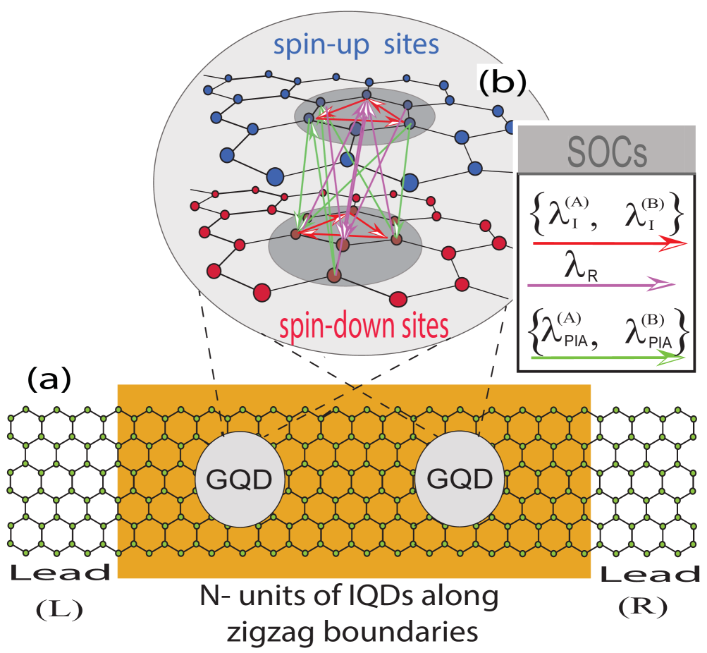
As mentioned above, we propose to study a chain of quantum dots with $C_{3v}$ symmetry in graphene created by proximity effects due to TMD islands. The choice of TMDs that conserve $C_{3v}$ symmetry is made to ensure the largest values of induced spin-dependent couplings in the graphene membrane [28, 35]. Such engineered IQDs will exhibit pseudohelical and valley-centered edge states with potential for device applications [34, 36]. The salient advantages of such structures are: 1) longer localization lengths for valley states in narrow ribbons, 2) valley Chern numbers and localization lengths independent of RSOCs, and 3) gapless band structures. A schematic picture of the system is shown in Fig. 1.
<details>
<summary>x1.png Details</summary>
### Visual Description
# Technical Document Extraction: Graphene Quantum Dot (GQD) System Diagram
This document provides a detailed technical extraction of the provided image, which illustrates a physical model of Graphene Quantum Dots (GQDs) embedded in a nanoribbon, focusing on Spin-Orbit Coupling (SOC) interactions.
## 1. Component Isolation
The image is divided into two primary sections:
* **Region (a) - Bottom:** A macroscopic/schematic view of the device geometry.
* **Region (b) - Top:** A microscopic/atomic-scale zoom-in of the electronic interactions within a GQD.
---
## 2. Region (a): Device Geometry and Setup
### Visual Description
This region shows a hexagonal lattice (graphene) nanoribbon. The central portion is highlighted with an orange rectangular background, containing two circular regions labeled "GQD". The ends of the ribbon extend into white backgrounds.
### Extracted Text and Labels
* **(a)**: Identifier for the bottom panel.
* **Lead (L)**: Located at the far left of the nanoribbon.
* **Lead (R)**: Located at the far right of the nanoribbon.
* **GQD**: Two circular grey regions within the orange central zone, representing Graphene Quantum Dots.
* **N- units of IQDs along zigzag boundaries**: Text located at the bottom center, describing the arrangement of the internal quantum dots along the zigzag edges of the nanoribbon.
### Structural Components
* **Lattice Structure**: A honeycomb (hexagonal) lattice representing graphene.
* **Central Region**: An orange-shaded area containing the active GQD components.
* **Boundary Type**: The text specifies "zigzag boundaries," which refers to the specific geometric termination of the graphene lattice edges.
---
## 3. Region (b): Microscopic Interaction Model
### Visual Description
A circular "zoom-in" (indicated by dashed lines from the GQDs in panel a) showing two parallel layers of hexagonal lattices. The top layer is blue, and the bottom layer is red. Various colored arrows represent different types of Spin-Orbit Coupling (SOC) interactions between the atoms.
### Extracted Text and Labels
* **(b)**: Identifier for the top panel.
* **spin-up sites**: Blue text labeling the top blue hexagonal lattice layer.
* **spin-down sites**: Red text labeling the bottom red hexagonal lattice layer.
### Legend: SOCs (Spin-Orbit Couplings)
Located at the middle-right of the image, this table defines the interaction types represented by colored arrows:
| Symbol | Arrow Color | Interaction Type / Description |
| :--- | :--- | :--- |
| $\{\lambda_{\text{I}}^{(A)}, \lambda_{\text{I}}^{(B)}\}$ | **Red** | Intrinsic SOC (Intra-layer, horizontal arrows within the same lattice). |
| $\lambda_{\text{R}}$ | **Purple** | Rashba SOC (Inter-layer, vertical/diagonal arrows connecting blue and red sites). |
| $\{\lambda_{\text{PIA}}^{(A)}, \lambda_{\text{PIA}}^{(B)}\}$ | **Green** | Pseudospin-Inversion Asymmetry (PIA) SOC (Inter-layer, diagonal arrows connecting different sublattices). |
### Interaction Flow and Trends
* **Intra-layer (Red Arrows):** These arrows form triangles within the same spin layer (e.g., connecting three blue sites or three red sites). This represents the intrinsic SOC acting within the A and B sublattices of a single spin species.
* **Inter-layer (Purple and Green Arrows):** These arrows bridge the gap between the "spin-up" (blue) and "spin-down" (red) layers.
* **Purple arrows ($\lambda_{\text{R}}$)**: Show direct vertical or near-vertical coupling between the layers, representing Rashba spin-orbit interaction.
* **Green arrows ($\lambda_{\text{PIA}}$)**: Show cross-coupling between the layers, representing the PIA term.
---
## 4. Summary of Technical Data
* **Material**: Graphene (indicated by the honeycomb lattice).
* **System**: Two Graphene Quantum Dots (GQDs) connected to Left (L) and Right (R) leads.
* **Physics Focus**: Spin-Orbit Couplings (SOCs) including Intrinsic ($\lambda_{\text{I}}$), Rashba ($\lambda_{\text{R}}$), and PIA ($\lambda_{\text{PIA}}$) terms.
* **Spin Modeling**: The system is modeled using two effective layers representing "spin-up" and "spin-down" degrees of freedom to visualize the SOC-induced transitions between them.
</details>
Figure 1: Panel (a) displays the overall device, which consists of a 2D graphene ribbon with zigzag boundaries decorated with semiconducting transition-metal dichalcogenide (TMD) islands. (b) Zoom-in of a quantum dot made of graphene and TMD. To visualize the emergence of different SOC terms, we duplicate the graphene membrane to emphasize the lift of the spin degeneracy. Each layer corresponds to a different spin component, with the blue (red) membrane representing the spin-up (spin-down) population. The induced SOCs combined with the underlying $C_{3v}$ symmetry give rise to sublattice-resolved intrinsic couplings $\lambda_{I}^{(A)},\ \lambda_{I}^{(B)}$ , denoted by red arrows, and pseudospin inversion-asymmetric couplings $\lambda_{PIA}^{(A)},\ \lambda_{PIA}^{(B)}$ denoted by green arrows. The Rashba $\lambda_{R}$ coupling is represented by purple arrows.
The deposition of adsorbates on graphene, or of graphene membranes on islands, results in profound changes in the electronic structure that depend on the locally conserved symmetries as described in Ref. [28]. The most important effects are the emergence of i) an effective staggered potential due to the broken reflection symmetry imposed by different orbital interactions experienced by the carbon atoms in proximity to the different atomic species of the TMD material and ii) several sublattice dependent next-nearest neighbor hopping terms originated from the proximity-induced spin-orbit interactions. In this case, the system can be described by an extension of the models by Kane and Mele [30] and Haldane [37]. The Hamiltonian for the QD regions is given by: [27, 28, 29, 38]
$$
\displaystyle H_{QD} \displaystyle=-t\sum_{\langle i,j\rangle}a_{is}^{\dagger}b_{js} \displaystyle+\sum_{\left\langle i\right\rangle} \displaystyle\Delta\left(\xi^{(A)}{\bf a}_{is}^{\dagger}{\bf a}_{is}+\xi^{(B)}%
{\bf b}_{is}^{\dagger}{\bf b}_{is}\right) \displaystyle+\Big{(}\frac{2i}{3}\Big{)} \displaystyle\sum_{\left\langle i,j\right\rangle\sigma,\sigma^{\prime}}\left(%
\lambda_{R}\ {\bf a}_{i\sigma}^{\dagger}{\bf b}_{j\sigma}\right)\left[{\bf\hat%
{s}}\otimes{\bf d}_{ij}\right]_{\sigma,\sigma^{\prime}} \displaystyle+\Big{(}\frac{i}{3\sqrt{3}}\Big{)} \displaystyle\sum_{\left\langle\left\langle i,j\right\rangle\right\rangle%
\sigma}\nu_{ij}\left(\lambda_{I}^{(A)}{\bf a}_{i\sigma}^{\dagger}{\bf a}_{j%
\sigma}+\lambda_{I}^{(B)}{\bf b}_{i\sigma}^{\dagger}{\bf b}_{j\sigma}\right)%
\left[{\bf\hat{s}}_{z}\right]_{\sigma,\sigma} \tag{1}
$$
where $t$ is the nearest neighbor hopping between sites $i$ and $j$ (note that these are spin-preserving processes). $\Delta$ is the staggered potential induced by the TMD islands in the dot region. This potential is sublattice-dependent with $\xi^{(A)}=1$ ( $\xi^{(B)}=-1$ ), rendering opposite signs for the induced gaps, i.e., $\Delta^{(A)}=-\Delta^{(B)}=\Delta$ for sublattice A (B). The Rashba interaction (RSOC) is expressed in terms of the coupling $\lambda_{R}$ . This coupling breaks the $z$ inversion symmetry while exchanging the spin of different sublattices. Here, the $\textbf{d}_{ij}$ vector connects site $j$ to $i$ . The terms $\lambda_{I}^{(A)}$ and $\lambda_{I}^{(B)}$ represent the intrinsic SOCs (ISOC) between next-nearest neighbors. These terms connect the same sublattices and spins in the clockwise ( $\nu_{ij}=-1$ ) or anticlockwise ( $\nu_{ij}=-1$ ) direction from site $j$ to site $i$ . Finally, the spin is denoted by the vector $\widehat{\textbf{s}}$ with components written in terms of Pauli matrices. It is worth restating that the SOCs exist only within the QD regions; outside the system is described by the Hamiltonian of pristine graphene.
Working with a Hamiltonian in reciprocal space is more convenient for studying valley properties. The resulting effective Hamiltonian is obtained by linearizing Eq. (1) around the ${\bf K_{1}}$ and ${\bf K_{2}}$ valleys labeled below by the valley index $\kappa=-1$ and $\kappa=+1$ , respectively. The final expression is given in the form $H_{QD}=H_{k}+H_{\Delta}+H_{R}+H_{I}$ [34], where:
$$
\displaystyle H_{k} \displaystyle= \displaystyle\hbar v_{F}\left(\kappa k_{x}\sigma_{x}+k_{y}\sigma_{y}\right)s_{%
0}, \displaystyle H_{\Delta} \displaystyle= \displaystyle\Delta\sigma_{z}s_{0}, \displaystyle H_{R} \displaystyle= \displaystyle\lambda_{R}\left(-\kappa\sigma_{x}s_{y}+\sigma_{y}s_{x}\right)s_{%
0}, \displaystyle H_{I} \displaystyle= \displaystyle(\kappa/2)\big{[}\lambda_{I}^{(A)}\left(\sigma_{z}+\sigma_{0}%
\right)+\lambda_{I}^{(B)}\left(\sigma_{z}-\sigma_{0}\right)\big{]}s_{z}. \tag{2}
$$
The Fermi velocity $v_{F}$ is expressed in terms of the hopping $t$ as $v_{F}=\sqrt{3}a_{0}t/2\hbar$ where $a_{0}$ is the lattice constant. The pseudospin is denoted by the Pauli matrices $\sigma$ , and $s_{0}$ denotes the spin identity matrix.
While Eqs.(2 - 5) provide an intuitive picture of the effect of each SOC term on the valleys, the results presented in the following sections are obtained by combining the S-matrix formalism with the tight-binding model for a zigzag terminated ribbon. This boundary condition preserves the valley quantum number and the valley topological properties of graphene. We compute the valley-polarized conductance with the Landauer-Büttiker approach:
$$
G_{\kappa}^{n,m}=(e^{2}/h)\left|S_{\kappa}^{n,m}\right|^{2},\qquad(n,\ m\equiv
L%
,R). \tag{6}
$$
Here $S_{\kappa}^{n,m}$ is the scattering matrix element between left (L) and right (R) leads for a given valley index ${\kappa}=± 1$ [39]. Thus, our calculations exploit the formalism with valley-dependent local currents as defined in Ref. [40]. Details regarding the computation of the valley conductance and currents are presented in Appendices A and B.
III Results
In this section, we present numerical results for the valley-polarized conductance for a range of structures that contain from a single IQD ( $n=1$ ) to a chain ( $n>1$ ) of IQDs. To emphasize the qualitative features resulting from the competition among the different interactions in the model, we adjust the parameters’ values accordingly to present the main findings. This procedure is usually applied to identify the role played by the various interactions [41, 34, 42]. We note, however, that for accurate setups, one expects weaker values for SOCs from proximity effects, and we address this situation in Sec. III.2.
III.1 Qualitative analysis of results
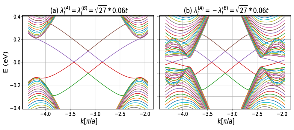
Following Refs. [30] and [34], we solve the model using the following ranges for the various SOC parameters: $\lambda_{R}≤ 0.075t$ and $\lambda_{I}^{(A)}=-\lambda_{I}^{(B)}≤\sqrt{27}0.06t$ in units of $t=1$ [34].
We consider $n$ symmetric quantum dots ( $n=1,2,3,4$ ), with the same spin-orbit parameters, arranged in a chain with the same radius $r_{0}=7$ nm and the space in-between them set to $d=5r_{0}$ . The circular geometry of the dots is chosen to preserve the symmetries of the original model and provide maximum localization of valley states, as discussed below. We set the incident energy at $E_{F}=0.035t$ and consider a ribbon width $w=30$ nm, with zigzag boundaries. For this range of ISOC values, the valley Zeeman effect is the most important term as the topological invariant $Z_{2}$ remains trivial, i.e., $Z_{2}=0$ and the bulk system is in the same topological phase as long as the ISOC is staggered, i.e., $\lambda_{I}^{(A)}=-\lambda_{I}^{(B)}$ [34, 36].
The reduced number of group symmetries of pristine graphene due to the proximity of the TMD island is reflected by the large number of lower-symmetry allowed SOC parameters. The effects of these couplings are observed in Fig, 2 (a, b), where the band structure near the two Dirac cones appears clearly modified. Fig. 2 (a) shows results in the absence (a) and presence (b) of a staggered potential. The changes include a newly open gap and additional edge bands resulting from the ISOC. These linear bands represent edge states that are unique to the staggered case $\lambda_{I}^{(A)}=-\lambda_{I}^{(B)}$ while they disappear in the uniform regime $\lambda_{I}^{(A)}=\lambda_{I}^{(B)}$ . Similar results have been found in Ref. [34] where more details about the valley selection and its related sublattice occupation are discussed. Based on these findings, a proximity effect that induces a staggered ISOC might lead to the emergence of valley currents and the localization of valley-centered sublattice polarized edge states. Indeed, these results manifest themselves in transport, providing valley states as conducting channels, as shown in Fig. 2 (b), an issue discussed in the coming subsections.
<details>
<summary>x2.png Details</summary>
### Visual Description
# Technical Data Extraction: Electronic Band Structure Plots
This document provides a detailed technical extraction of the data and visual information contained in the provided image, which consists of two side-by-side electronic band structure plots.
## 1. General Metadata and Global Axis
* **Image Type:** Scientific line plots (Band structure diagrams).
* **Y-Axis (Common):** Energy, labeled as **$E \text{ (eV)}$**.
* **Range:** $-0.4$ to $0.4$.
* **Major Tick Marks:** $-0.4, -0.2, 0.0, 0.2, 0.4$.
* **X-Axis (Common):** Wave vector, labeled as **$k [\pi/a]$**.
* **Range:** Approximately $-4.4$ to $-1.9$.
* **Major Tick Marks:** $-4.0, -3.5, -3.0, -2.5, -2.0$.
* **Grid:** Both plots feature a light gray rectangular grid aligned with the major tick marks.
---
## 2. Subplot (a) Analysis
**Header Label:** (a) $\lambda_I^{(A)} = \lambda_I^{(B)} = \sqrt{27} * 0.06t$
### Component Isolation & Trends
This plot shows a band structure with a clear energy gap and crossing states within that gap.
* **Bulk Bands (Top and Bottom):**
* **Conduction Bands (Top):** A dense manifold of parabolic-like curves starting around $E = 0.2 \text{ eV}$. They curve upward away from the center.
* **Valence Bands (Bottom):** A dense manifold of parabolic-like curves starting around $E = -0.2 \text{ eV}$. They curve downward away from the center.
* **Edge/Surface States (Crossing Lines):**
* There are four distinct linear bands that cross the band gap between $k = -4.0$ and $k = -2.0$.
* **Trend 1 (Positive Slope):** Two lines (one purple, one brown) slope upward from left to right. They cross $E = 0$ at approximately $k = -3.4$ and $k = -2.4$.
* **Trend 2 (Negative Slope):** Two lines (one red, one green) slope downward from left to right. They cross $E = 0$ at approximately $k = -3.4$ and $k = -2.4$.
* **Symmetry:** The plot is symmetric around the vertical line $k = -2.9$ (approximate center of the Brillouin zone shown).
---
## 3. Subplot (b) Analysis
**Header Label:** (b) $\lambda_I^{(A)} = -\lambda_I^{(B)} = \sqrt{27} * 0.06t$
### Component Isolation & Trends
This plot shows a significantly different topology compared to (a), characterized by a "pinched" or narrower gap and more complex oscillations in the bulk bands.
* **Bulk Bands (Top and Bottom):**
* The manifolds are much more spread out vertically compared to plot (a).
* **Oscillatory Behavior:** Near the gap edges (around $k = -4.0$ and $k = -2.3$), the bands exhibit "wavy" or oscillatory behavior rather than smooth parabolas.
* **Edge/Surface States (Crossing Lines):**
* Similar to (a), there are crossing linear bands in the center.
* **Trend 1 (Positive Slope):** A purple line and a brown line slope upward.
* **Trend 2 (Negative Slope):** A red line and a green line slope downward.
* **Key Difference:** The crossing points at $E = 0$ appear more compressed toward the center compared to plot (a). The "gap" between the bulk manifolds is narrower at the $k$ values where the edge states emerge.
* **Gap Structure:** The energy gap between the dense conduction and valence manifolds is significantly smaller in the regions between $k = -3.5$ and $k = -2.5$ compared to plot (a).
---
## 4. Comparative Summary
| Feature | Plot (a) | Plot (b) |
| :--- | :--- | :--- |
| **Parameter Relation** | $\lambda_I^{(A)} = \lambda_I^{(B)}$ | $\lambda_I^{(A)} = -\lambda_I^{(B)}$ |
| **Bulk Band Shape** | Smooth, parabolic manifolds. | Oscillatory/wavy manifolds near the gap. |
| **Energy Gap** | Wide and well-defined. | Narrower, with bulk states extending closer to $E=0$. |
| **Crossing States** | Clear linear crossings through a large vacuum. | Crossings exist but are surrounded by more complex bulk structures. |
**Technical Note:** These plots likely represent the band structure of a topological insulator or a similar 2D material (like a transition metal dichalcogenide or functionalized graphene) where $\lambda_I$ represents an intrinsic spin-orbit coupling parameter. The transition from (a) to (b) demonstrates how the relative sign of the coupling on different sublattices (A and B) alters the topological protection and the dispersion of the edge states.
</details>
<details>
<summary>x3.png Details</summary>
### Visual Description
# Technical Data Extraction: Conductance (G) vs. Spin-Orbit Coupling ($\lambda_I/t$)
This document provides a comprehensive extraction of the data and trends presented in the provided scientific plot, which illustrates the conductance properties of a physical system (likely a topological insulator or graphene-based nanostructure) under varying parameters.
## 1. Metadata and Global Parameters
The image contains a header with specific physical constants used for the simulation:
* **Figure Label:** (c)
* **Rashba Spin-Orbit Coupling ($\lambda_R$):** $0.015t$
* **Exchange Field/Gap ($\Delta$):** $0.005t$
* **Fermi Energy ($E_F$):** $+0.035t$
* **Units:** Conductance is measured in units of $e^2/\hbar$. The x-axis is a dimensionless ratio $\lambda_I/t$.
---
## 2. Main Plot Analysis (Left Panel)
The left panel shows the conductance $G$ as a function of $\lambda_I/t$ ranging from $0.00$ to approximately $0.13$. It is divided into two vertically stacked regions labeled $K_1$ and $K_2$.
### Component Isolation
* **Region $K_1$ (Top):** Conductance values range from $2.0$ to $4.0$.
* **Region $K_2$ (Bottom):** Conductance values range from $0.0$ to $2.0$.
* **Legend (Top Right):** Located at approximately $[x=0.4, y=0.1]$ relative to the left panel's top-right corner.
* **Black line:** $n=1$
* **Blue line:** $n=2$
* **Red line:** $n=3$
* **Green line:** $n=4$
### Data Trends and Observations
1. **Initial State ($\lambda_I/t = 0$):** All lines start at quantized values. In $K_1$, $G \approx 4.0$. In $K_2$, $G \approx 2.0$.
2. **Oscillatory Behavior:** The conductance exhibits periodic "dips" and "peaks." Major peaks occur near $\lambda_I/t \approx 0.05, 0.10,$ and $0.13$.
3. **Effect of $n$:**
* **$n=1$ (Black):** Shows the smoothest transitions and highest baseline conductance between peaks. It acts as an upper envelope for the other series.
* **$n=2, 3, 4$ (Blue, Red, Green):** As $n$ increases, the conductance drops more sharply toward zero (in $K_2$) or toward $2.0$ (in $K_1$) in the regions between peaks.
* **Trend:** Higher $n$ values result in more pronounced oscillations and sharper features.
---
## 3. Zoomed Analysis (Right Panels)
Two sub-plots provide high-resolution views of the transition region near $\lambda_I/t \approx 0.06$.
### Sub-plot: "a zoom in $K_2$" (Middle)
* **X-axis range:** $\approx 0.052$ to $0.068$
* **Y-axis range:** $0.0$ to $1.3$
* **Trend Verification:**
* **Black ($n=1$):** Slopes downward monotonically from $\approx 1.05$ to $\approx 0.45$.
* **Blue ($n=2$):** Slopes downward with a slight shoulder near $0.060$, dropping sharply after $0.062$.
* **Red ($n=3$):** Exhibits a distinct local peak at $\approx 0.063$ before dropping.
* **Green ($n=4$):** Exhibits the most complex behavior with two distinct oscillations/peaks between $0.055$ and $0.065$ before a sharp vertical-like drop at $0.065$.
### Sub-plot: "a zoom in $K_1$" (Right)
* **X-axis range:** $\approx 0.052$ to $0.068$
* **Y-axis range:** $2.0$ to $3.2$
* **Trend Verification:**
* This plot mirrors the behavior of the $K_2$ zoom but shifted upward by exactly $2.0$ units of $e^2/\hbar$.
* **Black ($n=1$):** Starts at $\approx 3.05$, ends at $\approx 2.45$.
* **Green ($n=4$):** Shows a sharp resonance peak reaching $G=3.0$ at $\lambda_I/t \approx 0.065$.
---
## 4. Summary Table of Key Data Points (Approximate)
| $\lambda_I/t$ Value | Feature | $K_2$ Conductance ($n=4$, Green) | $K_1$ Conductance ($n=4$, Green) |
| :--- | :--- | :--- | :--- |
| 0.00 | Origin | 2.0 | 4.0 |
| 0.02 - 0.04 | First Trough | $\approx 0.0$ | $\approx 2.0$ |
| 0.05 | First Major Peak | $\approx 1.0$ | $\approx 3.0$ |
| 0.065 | Resonance (Zoom) | Sharp Peak to $\approx 1.0$ | Sharp Peak to $\approx 3.0$ |
| 0.08 | Second Trough | $\approx 0.0$ | $\approx 2.0$ |
| 0.10 | Second Major Peak | $\approx 1.0$ | $\approx 3.0$ |
---
## 5. Conclusion
The data indicates a perfectly synchronized conductance behavior between the $K_1$ and $K_2$ valleys, differing only by a constant offset of $2 e^2/\hbar$. The parameter $n$ controls the sharpness of the conductance quantization, with higher $n$ leading to more rapid switching between conducting and non-conducting states as the intrinsic spin-orbit coupling ($\lambda_I$) is tuned.
</details>
<details>
<summary>x4.png Details</summary>
### Visual Description
# Technical Data Extraction: Conductance (G) vs. $\lambda_I/t$
This document provides a comprehensive extraction of data and trends from the provided scientific plot, which illustrates the conductance ($G$) in units of $e^2/\hbar$ as a function of the dimensionless parameter $\lambda_I/t$.
## 1. Metadata and Global Parameters
The image contains a header indicating the physical parameters held constant for these simulations:
* **Figure Label:** (d)
* **Rashba Coupling ($\lambda_R$):** $0.015t$
* **Exchange/Gap Parameter ($\Delta$):** $0.005t$
* **Fermi Energy ($E_F$):** $-0.035t$
## 2. Main Plot Analysis (Left Panel)
The left panel displays two vertically stacked regions labeled $K_1$ and $K_2$, sharing a common x-axis.
### Axis Definitions
* **X-axis:** $\lambda_I/t$, ranging from $0.00$ to approximately $0.13$.
* **Y-axis:** Conductance $G$ ($e^2/\hbar$).
* **$K_1$ Region (Bottom):** Values range from $0.0$ to $2.0$.
* **$K_2$ Region (Top):** Values range from $2.0$ to $4.0$.
### Legend and Data Series (Spatial Grounding: Top Right of Main Plot)
Four data series are plotted, distinguished by color and the integer parameter $n$:
1. **Black Line ($n=1$):** Shows the smoothest oscillations with the highest minimum conductance values.
2. **Blue Line ($n=2$):** Shows deeper oscillations than $n=1$.
3. **Red Line ($n=3$):** Shows even deeper oscillations and begins to exhibit sharp "dips" or resonances.
4. **Green Line ($n=4$):** Shows the most extreme oscillations, reaching near-zero conductance in the $K_1$ region and near $2.0$ in the $K_2$ region.
### Visual Trends and Observations
* **Periodicity:** The conductance exhibits a periodic "wavy" pattern. Major peaks occur near $\lambda_I/t \approx 0.00, 0.055, 0.105$.
* **Symmetry:** The $K_2$ plot appears to be a vertical translation of the $K_1$ plot (shifted up by $2.0$ units).
* **Resonance Features:** Between $\lambda_I/t = 0.06$ and $0.07$, and again between $0.11$ and $0.12$, the $n=3$ (red) and $n=4$ (green) lines show rapid, sharp fluctuations (Fano-like resonances).
---
## 3. Zoomed-In Analysis (Right Panels)
Two sub-plots provide high-resolution views of the resonance regions for $K_1$ and $K_2$.
### Sub-plot: "a zoom in $K_1$"
* **X-axis:** $\lambda_I/t$ from $0.052$ to $0.068$.
* **Y-axis:** $G$ ($e^2/\hbar$) from $0.0$ to $1.5$.
* **Trend Verification:**
* **Black ($n=1$):** Slopes downward monotonically from $\approx 1.05$ to $\approx 0.45$.
* **Blue ($n=2$):** Slopes downward with a slight inflection, ending near $0.15$.
* **Red ($n=3$):** Oscillates; peaks at $\approx 1.0$ near $0.063$, then drops sharply.
* **Green ($n=4$):** Highly oscillatory; shows a sharp peak reaching $\approx 1.0$ at $\lambda_I/t \approx 0.065$ before a vertical-like drop toward zero.
### Sub-plot: "a zoom in $K_2$"
* **X-axis:** $\lambda_I/t$ from $0.052$ to $0.068$.
* **Y-axis:** $G$ ($e^2/\hbar$) from $2.0$ to $3.2$.
* **Trend Verification:**
* **Black ($n=1$):** Slopes downward from $\approx 3.05$ to $\approx 2.45$.
* **Blue ($n=2$):** Peaks at $\approx 3.0$ near $0.058$, then drops to $\approx 2.15$.
* **Red ($n=3$):** Peaks at $\approx 3.0$ near $0.063$, then drops.
* **Green ($n=4$):** Shows two distinct peaks; the second is very sharp, reaching $\approx 3.0$ at $\lambda_I/t \approx 0.065$.
---
## 4. Data Summary Table (Approximate Values)
| $\lambda_I/t$ (approx) | $G$ ($K_1, n=4$) | $G$ ($K_2, n=4$) | Feature Description |
| :--- | :--- | :--- | :--- |
| 0.00 | 2.0 | 4.0 | Global Maximum |
| 0.03 | 0.0 | 2.0 | Local Minimum (Broad) |
| 0.055 | 1.0 | 3.0 | Local Maximum |
| 0.065 | 1.0 (sharp) | 3.0 (sharp) | Resonance Peak |
| 0.08 | 0.0 | 2.0 | Local Minimum (Broad) |
| 0.105 | 1.0 | 3.0 | Local Maximum |
| 0.115 | 1.0 (sharp) | 3.0 (sharp) | Resonance Peak |
**Note on Language:** All text in the image is in English using standard mathematical notation. No other languages are present.
</details>
<details>
<summary>x5.png Details</summary>
### Visual Description
# Technical Data Extraction: Conductance Plots (e) and (f)
This document provides a detailed technical extraction of the data and trends presented in the two provided line charts, which appear to be from a physics research paper regarding electronic transport properties.
## 1. Global Parameters
Both charts share the following physical parameters, as indicated in their respective headers:
* **$\lambda_R = \lambda_I = 0.015t$**: Spin-orbit coupling parameters.
* **$\Delta = 0.005t$**: Superconducting gap or exchange field parameter.
* **$E_F = 0.035t$**: Fermi energy level.
* **Y-Axis (Common):** Conductance $G$ in units of $(e^2/h)$. The scale ranges from $0.0$ to $3.0$ with major ticks every $0.5$.
---
## 2. Chart (e) Analysis
### Metadata and Labels
* **Header:** (e) $\lambda_R = \lambda_I = 0.015t, \Delta = 0.005t, E_F = 0.035t$
* **X-Axis Title:** $d/r_0$ (Dimensionless ratio of distance to a reference radius).
* **X-Axis Range:** $0$ to $10$.
* **Legend Location:** Top right $[x \approx 0.9, y \approx 0.9]$.
* **Red Square ($\square$):** $K_1$
* **Blue Circle ($\bullet$):** $K_2$
### Data Trends and Values
The data is represented by dashed black lines connecting the markers.
#### Series $K_1$ (Red Squares)
* **Trend:** Initially decreases from $d/r_0 = 1$ to $3$, reaching a minimum near zero. It then sharply increases between $d/r_0 = 3$ and $5$, plateauing at a constant value for $d/r_0 \ge 5$.
* **Key Data Points:**
* $d/r_0 = 1$: $G \approx 0.75$
* $d/r_0 = 2$: $G \approx 0.6$
* $d/r_0 = 3$: $G \approx 0.1$ (Minimum)
* $d/r_0 = 4$: $G \approx 1.5$
* $d/r_0 = 5$ to $10$: $G = 2.0$ (Stable Plateau)
#### Series $K_2$ (Blue Circles)
* **Trend:** Remains very low (near zero) throughout the range, with a small localized peak at $d/r_0 = 4$.
* **Key Data Points:**
* $d/r_0 = 1$ to $3$: $G \approx 0.1$
* $d/r_0 = 4$: $G \approx 0.5$ (Localized Peak)
* $d/r_0 = 5$ to $10$: $G \approx 0.05$ (Near-zero baseline)
---
## 3. Chart (f) Analysis
### Metadata and Labels
* **Header:** (f) $\lambda_R = \lambda_I = 0.015t, \Delta = 0.005t, E_F = 0.035t$
* **Inset Text:** $d = 5r_0$ (Indicates this plot is a cross-section or specific case where the ratio from chart (e) is fixed at 5).
* **X-Axis Title:** $n$ (Likely an index or number of units).
* **X-Axis Range:** $0$ to $10$.
* **Legend Location:** Top right $[x \approx 0.9, y \approx 0.9]$.
* **Red Square ($\square$):** $K_1$
* **Blue Circle ($\bullet$):** $K_2$
### Data Trends and Values
The data is represented by dashed black lines connecting the markers.
#### Series $K_1$ (Red Squares)
* **Trend:** Perfectly horizontal line. The conductance is invariant with respect to $n$.
* **Data Points:**
* $n = 0$ to $10$: $G = 2.0$ (Constant)
#### Series $K_2$ (Blue Circles)
* **Trend:** Perfectly horizontal line at the baseline.
* **Data Points:**
* $n = 0$ to $10$: $G = 0.0$ (Constant)
---
## 4. Summary Comparison
* **Chart (e)** shows the transition of conductance as the spatial parameter $d/r_0$ increases. It reveals a critical transition point at $d/r_0 = 5$, where $K_1$ reaches a quantized conductance of $2.0$ and $K_2$ drops to zero.
* **Chart (f)** confirms that once the system is at the state $d = 5r_0$, the conductance values for $K_1$ and $K_2$ are stable and quantized ($2$ and $0$ respectively) regardless of the parameter $n$.
</details>
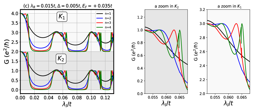
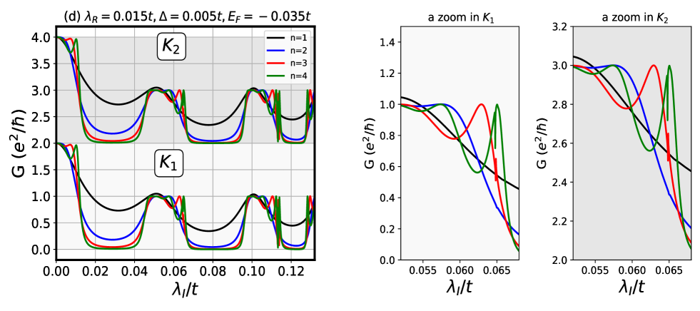
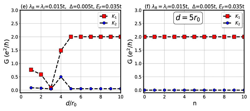
Figure 2: Energy bands for uniform $\lambda_{I}^{(A)}=\lambda_{I}^{(B)}$ (a), and staggered $\lambda_{I}^{(A)}=-\lambda_{I}^{(B)}$ ) (b) for a 30 nm wide zigzag ribbon, $\Delta=0.1t$ and $\lambda_{R}=0.075t$ . Panels (c) and (d) show valley conductances vs intrinsic spin-orbit length $\lambda_{I}$ for several IQDs with staggered ISOC. Narrow panels on the right correspond to zoom-ins for each valley as a function of $\lambda_{I}$ . Panels (e) and (f) correspond to conductance vs inter-dot spacing $d$ and number $n$ of IQDs.
III.1.1 Valley-dependent conductance through proximity IQDs
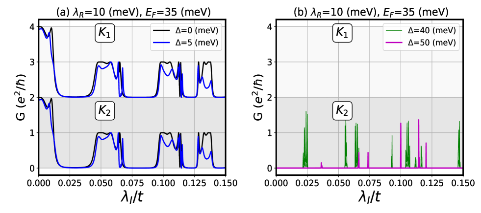
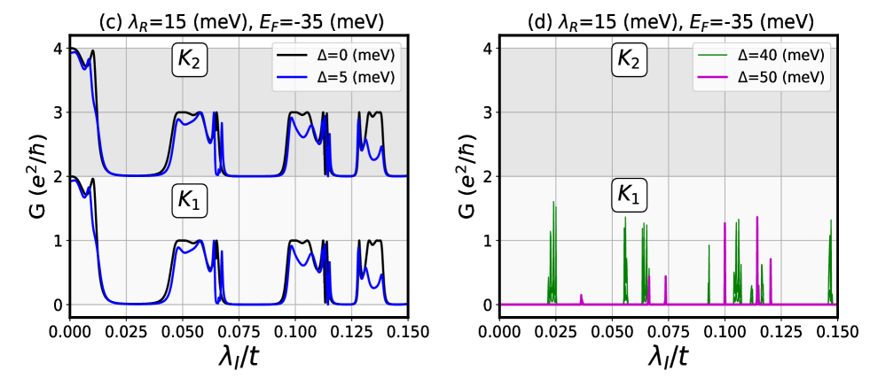
Figure 2 (c) and (d) display the conductance through a group of $n$ symmetric quantum dots with staggered ISOC. One interesting observation is the approximately square-type dependence revealing wide gaps that can be made more pronounced by changing the strength of ISOC for $n≥ 3$ QDs. We observe that $100\%$ ( $0\%$ ) of the detected conductance results from the flow of electrons through the $\kappa=-1$ ( $\kappa=+1$ ) valley for positive incident energy ( $E_{F}=0.035t$ ), while $0\%$ ( $100\%$ ) occurs for negative incident energy ( $E_{F}=-0.035t$ ). The opposite behavior is obtained for the complementary valley. Interestingly, the gaps occur at different ranges of ISOC values, with the emerging valley-polarized current being switched from one valley to the other within the gap region by an appropriate change of $E_{F}$ . Furthermore, we observe a decrease in the widths of the gaps with increasing SOC strength, which suggests they might vanish for high enough values of ISOC.
An analysis of Figs. 2 (c) and (d) reveal resonances in the transmittance at around the value $\lambda_{I}=0.065t$ , with the spectrum in the zoom-in panels showing that the IQDs confine electrons with index $\kappa=+1$ ( $\kappa=-1$ ) at positive (negative) energy. Hence, the scattering through the IQD region tends to zero accordingly. We observe that the number and sharpness of the resonance weakly depend on the number of IQDs along the chain, as seen for $n=1,2,3$ curves that present at least one resonant state each at similar values of ISOCs. More details about the observed confinement are addressed below in Sec. III.2.3, and we discuss these results, including realistic parameters, in III.3.
Additionally, the conductance response shows several interesting characteristics: (1) It exhibits an oscillating behavior that becomes more pronounced with increasing $n$ . In this case, the conductance oscillations arise from mode mixing, and their number depends on the number $n$ of the IQDs, as shown in the zoom-in of Fig. 2 (c) and (d). (2) The conductance plateaux become better defined as $n$ increases ( $n≥ 3$ ), with values $G(\kappa=+1)=0$ and $G(\kappa=-1)=2G_{0}$ for panel (c) and $G(\kappa=+1)=2G_{0}$ and $G(\kappa=-1)=0$ for panel (d).
These results suggest that the conductance plateaux are due to states that become valley polarized at specific strengths of the staggered ISOC, e.g., in the range $0.015t$ $≤\lambda_{I}^{(A)}=-\lambda_{I}^{(B)}≤ 0.04t$ as shown in Fig. 2 (c). Interestingly, when $E_{F}$ is negative, the valley polarization is reversed, as shown in panel (d) within the same range of values for $\lambda_{I}$ . Consequently, the transmitted current can be made to be valley polarized from either one of the two Dirac points ${\bf K_{1}}$ or ${\bf K_{2}}$ depending on the incident energy.
III.1.2 Dependence on coherent inter-dot electron transfer
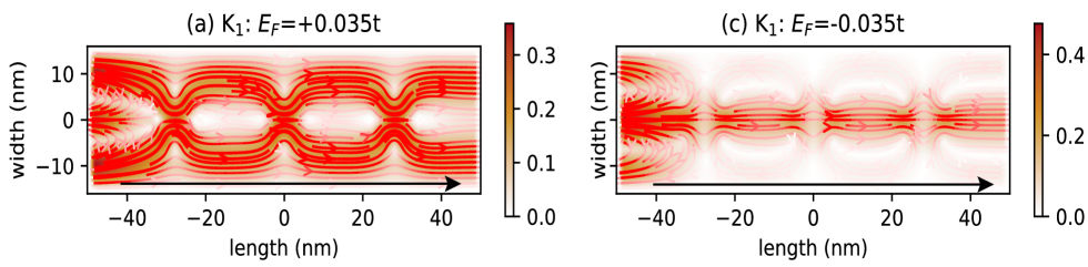
Within the conductance gap regions in Fig. 2 (c) and (d), and depending on the bias defined by the sign of the Fermi energy, the valley that appears in the output with $T=1$ seems to be barely scattered by the IQDs irrespective of the number of dots in the chain. Inversely, the states from the valley that appear in the output with $T=0$ are strongly reflected by the IQDs even for the shortest chain furnished by only one dot. To better understand these current profiles, we plot in Fig. 3 the local valley current through a chain of three IQDs. As the figures show, the transferred valley current is due to electron scattering processes that involve inter-dot hoppings between neighboring dots, as illustrated in the figure, that display uniform local densities everywhere between the dots for both valleys (Fig. 3 (a) and (d)). Notice also that in this case, the conductance is practically the same as for the zigzag terminated graphene ribbon with one or more quantum dots, as depicted in Fig. 2 (f).
<details>
<summary>x6.png Details</summary>
### Visual Description
# Technical Data Extraction: Current Density Streamline Plots
This document provides a detailed technical extraction of the data and visual components from the provided image, which consists of two side-by-side streamline plots representing physical simulations (likely electron transport in a nanostructure).
## 1. General Layout and Metadata
The image contains two subplots, labeled **(a)** and **(c)**. Both plots share the same spatial dimensions and coordinate system.
* **Language:** English
* **Horizontal Axis (x):** `length (nm)`
* **Range:** -50 to 50 nm
* **Markers:** -40, -20, 0, 20, 40
* **Vertical Axis (y):** `width (nm)`
* **Range:** -15 to 15 nm (approximate)
* **Markers:** -10, 0, 10
* **Color Scale (Legend):** Located to the right of each plot. It represents a normalized intensity or magnitude.
* **Color Gradient:** White (0.0) $\rightarrow$ Light Orange $\rightarrow$ Dark Red/Brown (0.6+)
* **Scale Markers:** 0.0, 0.2, 0.4, 0.6
---
## 2. Subplot (a) Analysis
**Header Label:** (a) $K_1: E_F = +0.035t$
### Component Isolation
* **Physical Context:** This plot represents a state with positive Fermi energy ($E_F$).
* **Visual Trend:** The streamlines originate from the left boundary ($x \approx -50$) and propagate toward the right. The intensity (indicated by the red/orange background) is sustained across the entire length of the channel.
* **Flow Pattern:**
* **Injection Point:** High intensity (dark red) at the left boundary, concentrated around $y = \pm 10$ and $y = 0$.
* **Central Region:** The flow exhibits a "braided" or undulating pattern. There are clear nodes of lower intensity (white spots) centered at approximately $x = -35$, $x = -15$, and $x = 25$.
* **Transmission:** The streamlines continue through the right boundary ($x = 50$), indicating high transmission/conductivity.
* **Color/Magnitude Data:**
* Peak values ($\approx 0.5$) are found at the injection site ($x = -50$).
* The intensity remains relatively high (orange hue, $\approx 0.2 - 0.3$) even at the far right of the plot.
---
## 3. Subplot (c) Analysis
**Header Label:** (c) $K_1: E_F = -0.035t$
### Component Isolation
* **Physical Context:** This plot represents a state with negative Fermi energy ($E_F$).
* **Visual Trend:** Unlike subplot (a), the flow in this plot is heavily attenuated. While it starts with high intensity on the left, it fades to near-zero (white) before reaching the center of the channel.
* **Flow Pattern:**
* **Injection Point:** High intensity (dark red) at the left boundary, similar to plot (a).
* **Decay:** The streamlines and the background color intensity drop sharply as $x$ increases.
* **Cut-off:** By $x = 0$, the intensity is nearly 0.0 (white). The streamlines become faint and disappear.
* **Transmission:** There is virtually no flow reaching the right boundary ($x = 50$), indicating a "blocked" or non-conducting state.
* **Color/Magnitude Data:**
* Peak values ($\approx 0.6$) are concentrated at the very edge of the left boundary ($x = -50$).
* The intensity drops below $0.1$ by $x = -20$.
---
## 4. Comparative Summary
| Feature | Subplot (a) | Subplot (c) |
| :--- | :--- | :--- |
| **Fermi Energy ($E_F$)** | $+0.035t$ (Positive) | $-0.035t$ (Negative) |
| **Propagation** | Long-range (Full length) | Short-range (Decays rapidly) |
| **Right Boundary State** | Conducting / Active | Non-conducting / Evanescent |
| **Max Intensity** | $\approx 0.5$ | $\approx 0.6$ (at source only) |
| **Visual Indicators** | Sustained orange/red background | Rapid transition to white background |
**Directional Indicator:** Both plots contain a black arrow at the bottom pointing from left to right, confirming the intended direction of transport or the orientation of the nanostructure.
</details>
<details>
<summary>x7.png Details</summary>
### Visual Description
# Technical Data Extraction: Current Density and Streamline Plots
This document provides a detailed technical extraction of the data and visual components from the provided image, which consists of two side-by-side heatmaps with overlaid streamlines, likely representing electronic transport properties in a nanostructure.
## 1. General Metadata
* **Language:** English
* **Image Type:** Scientific Heatmaps / Streamline Plots
* **Coordinate System:** Cartesian (Length vs. Width)
* **Units:** Nanometers (nm) for spatial dimensions; $t$ (hopping parameter) for energy.
---
## 2. Component Isolation: Plot (b)
### Header Information
* **Label:** (b)
* **Title:** $K_2: E_F = +0.035t$
* **Interpretation:** This plot represents the $K_2$ valley/state at a positive Fermi energy of $0.035t$.
### Axis Configuration
* **Y-axis (Left):** "width (nm)"
* **Range:** -10 to 10 (with visible ticks at -10, 0, 10).
* **X-axis (Bottom):** "length (nm)"
* **Range:** -40 to 40 (with visible ticks at -40, -20, 0, 20, 40).
* **Directional Indicator:** A black arrow at the bottom of the plot area points from left to right (negative to positive length).
### Colorbar (Legend)
* **Location:** Right side of plot (b).
* **Scale:** Linear, from 0.0 to 0.6.
* **Color Gradient:** White (0.0) $\rightarrow$ Light Orange $\rightarrow$ Dark Brown/Rust (0.6).
* **Function:** Represents the magnitude of a physical quantity (likely current density).
### Data Visualization & Trends
* **Heatmap Trend:** The highest intensity (dark orange/brown, $\approx 0.4 - 0.5$) is concentrated on the far left side (length $\approx -50$ to $-40$ nm) near the center and edges of the width. The intensity decays rapidly as length increases. By length $= 0$ nm, the intensity is nearly zero (white).
* **Streamlines:** Blue lines with arrows indicate flow direction.
* **Pattern:** On the left, there are circular/vortex-like patterns.
* **Flow:** The flow appears to enter from the left, circulate in the region between -50 and -20 nm, and then dissipate.
---
## 3. Component Isolation: Plot (d)
### Header Information
* **Label:** (d)
* **Title:** $K_2: E_F = -0.035t$
* **Interpretation:** This plot represents the $K_2$ valley/state at a negative Fermi energy of $-0.035t$.
### Axis Configuration
* **Y-axis (Left):** "width (nm)"
* **Range:** -10 to 10 (ticks at -10, 0, 10).
* **X-axis (Bottom):** "length (nm)"
* **Range:** -40 to 40 (ticks at -40, -20, 0, 20, 40).
* **Directional Indicator:** A black arrow at the bottom points from left to right.
### Colorbar (Legend)
* **Location:** Right side of plot (d).
* **Scale:** Linear, from 0.0 to 0.4 (Note: The peak scale is lower than in plot b).
* **Color Gradient:** White (0.0) $\rightarrow$ Light Orange $\rightarrow$ Dark Brown/Rust (0.4).
### Data Visualization & Trends
* **Heatmap Trend:** Unlike plot (b), the intensity in plot (d) is sustained across the entire length of the channel.
* **Left Region (-50 to -30 nm):** High intensity (dark orange, $\approx 0.3 - 0.4$) near the top and bottom edges.
* **Central/Right Region (-20 to 50 nm):** The intensity fluctuates but remains significant ($\approx 0.1 - 0.2$), showing a "beating" or oscillatory pattern along the length.
* **Streamlines:** Blue lines with arrows.
* **Pattern:** Shows a more laminar, forward-moving flow compared to plot (b).
* **Flow:** The streamlines originate at the left and propagate through the entire length to the right boundary, following a wavy path that corresponds to the intensity fluctuations in the heatmap.
---
## 4. Comparative Summary
| Feature | Plot (b) $E_F = +0.035t$ | Plot (d) $E_F = -0.035t$ |
| :--- | :--- | :--- |
| **Max Intensity** | $\approx 0.6$ (Higher) | $\approx 0.4$ (Lower) |
| **Spatial Decay** | High; signal vanishes by $x=0$. | Low; signal persists to $x=50$. |
| **Flow Character** | Localized vortices/backflow. | Extended propagation/forward flow. |
| **Symmetry** | Concentrated at the injection point. | Distributed throughout the nanostructure. |
**Conclusion:** The data indicates a strong asymmetry in transport for the $K_2$ state depending on the sign of the Fermi energy. Positive $E_F$ results in localized, non-propagating states, while negative $E_F$ allows for extended propagation across the length of the device.
</details>
<details>
<summary>x8.png Details</summary>
### Visual Description
# Technical Data Extraction: Current Density Streamline Plots
This document provides a detailed technical extraction of the data and visual information contained in the provided image, which consists of two side-by-side heatmaps with overlaid streamlines, likely representing electron current flow in a nanostructure.
## 1. General Metadata
* **Language:** English
* **Image Type:** Scientific Heatmaps / Streamline Plots
* **Coordinate System:** Cartesian 2D (Length vs. Width)
* **Units:** Nanometers (nm) for spatial dimensions; dimensionless or normalized units for intensity.
---
## 2. Component Isolation
### Region A: Left Plot (e)
* **Header Label:** (e) $K_1: E_F = +0.035t$
* **X-Axis Title:** length (nm)
* **X-Axis Markers:** -40, -20, 0, 20, 40
* **Y-Axis Title:** width (nm)
* **Y-Axis Markers:** -10, 0, 10
* **Color Bar (Legend):** Located at the right of the plot.
* **Range:** 0.0 to 0.6+
* **Color Gradient:** White (0.0) $\rightarrow$ Light Orange $\rightarrow$ Dark Red/Brown (~0.6)
* **Visual Trend:**
* The intensity is concentrated heavily on the right side of the plot (length > 30 nm).
* The left side of the plot (length < 20 nm) shows near-zero intensity (white).
* Streamlines (red arrows) originate from the right boundary and flow toward the left.
* A long black arrow at the bottom (width $\approx$ -13 nm) points from right to left, indicating the global direction of flow.
### Region B: Right Plot (g)
* **Header Label:** (g) $K_1: E_F = -0.035t$
* **X-Axis Title:** length (nm)
* **X-Axis Markers:** -40, -20, 0, 20, 40
* **Y-Axis Title:** width (nm)
* **Y-Axis Markers:** -10, 0, 10
* **Color Bar (Legend):** Located at the right of the plot.
* **Range:** 0.0 to 0.4+
* **Color Gradient:** White (0.0) $\rightarrow$ Light Orange $\rightarrow$ Dark Red/Brown (~0.4)
* **Visual Trend:**
* Intensity is distributed across the entire length of the channel.
* There is a high-intensity "source" region on the far right (length $\approx$ 50 nm) reaching values $> 0.4$.
* The flow exhibits periodic or quasi-periodic fluctuations in intensity along the length, with "nodes" of lower intensity (white/light orange) around length = 25 nm and length = -10 nm.
* Streamlines (red arrows) flow from right to left across the entire domain.
* A long black arrow at the bottom (width $\approx$ -13 nm) points from right to left.
---
## 3. Comparative Analysis
| Feature | Plot (e) | Plot (g) |
| :--- | :--- | :--- |
| **Fermi Energy ($E_F$)** | $+0.035t$ (Positive) | $-0.035t$ (Negative) |
| **Max Intensity Scale** | $\approx 0.6$ | $\approx 0.4$ |
| **Spatial Distribution** | Highly localized to the right edge. | Distributed throughout the channel. |
| **Flow Direction** | Right to Left | Right to Left |
| **Decay Pattern** | Rapid decay moving left from the source. | Oscillatory/Slow decay moving left. |
---
## 4. Detailed Streamline and Flow Description
### Plot (e) - Positive Fermi Energy
* **Source Region:** The highest current density (dark red, ~0.6) is centered at length = 50 nm, width = 0 nm.
* **Flow Pattern:** Streamlines fan out from the right edge. They are most dense and turbulent-looking near the center (width = 0) and curve toward the top and bottom edges before quickly fading into the white background as they move left.
* **Effective Range:** The signal effectively vanishes (reaches 0.0 on the color scale) by length = 20 nm.
### Plot (g) - Negative Fermi Energy
* **Source Region:** Similar to (e), the highest density is at the right boundary (length = 50 nm).
* **Flow Pattern:** The streamlines are more laminar and persistent. They extend the full length of the displayed area (-50 nm to 50 nm).
* **Interference/Nodes:** There are distinct regions of lower density (white spots) centered at approximately:
* [Length: 25 nm, Width: 0 nm]
* [Length: -15 nm, Width: 0 nm]
* **Edge Effects:** The current density appears slightly higher near the top and bottom edges (width $\pm$ 10 nm) compared to the central axis in certain segments, suggesting edge-state transport or interference patterns.
---
## 5. Textual Transcription
**Plot (e) Labels:**
* Title: `(e) K₁: E_F=+0.035t`
* Y-axis: `width (nm)`
* X-axis: `length (nm)`
* Colorbar Ticks: `0.0, 0.2, 0.4, 0.6`
**Plot (g) Labels:**
* Title: `(g) K₁: E_F=-0.035t`
* Y-axis: `width (nm)`
* X-axis: `length (nm)`
* Colorbar Ticks: `0.0, 0.2, 0.4`
</details>
<details>
<summary>x9.png Details</summary>
### Visual Description
# Technical Data Extraction: Current Density and Streamline Plots
This document provides a detailed technical extraction of the data contained in the provided image, which consists of two side-by-side scientific plots (labeled 'f' and 'h') representing physical simulations of current flow in a nanostructure.
## 1. General Metadata
* **Language:** English
* **Subject Matter:** Condensed Matter Physics / Nanotechnology (likely related to Graphene or Topological Insulators given the $K_2$ and $E_F$ notation).
* **Components:** Two heatmaps with overlaid vector streamlines and associated color bars.
---
## 2. Plot (f) Analysis
### Header and Labels
* **Title:** (f) $K_2$: $E_F = +0.035t$
* **Y-Axis Title:** width (nm)
* **Y-Axis Markers:** -10, 0, 10
* **X-Axis Title:** length (nm)
* **X-Axis Markers:** -40, -20, 0, 20, 40
### Color Bar (Legend)
* **Location:** Right side of plot (f).
* **Scale:** Linear heatmap ranging from white (0.0) to dark orange/brown (approx. 0.5).
* **Markers:** 0.0, 0.2, 0.4.
### Data Trends and Components
* **Heatmap (Background):** Represents a scalar quantity (likely current density magnitude). The intensity is highest (dark orange) on the right side (length $\approx$ 40 to 50 nm) and shows periodic "hotspots" or nodes along the center line ($y=0$) at approximately $x = -30, 0, 30$ nm.
* **Streamlines (Blue Lines):** Represent the direction of flow.
* **Trend:** The flow enters from the right and moves toward the left.
* **Behavior:** On the right side ($x > 30$), there is significant turbulence or vortex-like behavior where lines curve sharply. As the flow moves toward the left ($x < 0$), the streamlines become more laminar and parallel to the x-axis.
* **Directional Indicator:** A long black arrow at the bottom of the plot points from right to left (from $x \approx 40$ to $x \approx -50$), confirming the net direction of transport.
---
## 3. Plot (h) Analysis
### Header and Labels
* **Title:** (h) $K_2$: $E_F = -0.035t$
* **Y-Axis Title:** width (nm)
* **Y-Axis Markers:** -10, 0, 10
* **X-Axis Title:** length (nm)
* **X-Axis Markers:** -40, -20, 0, 20, 40
### Color Bar (Legend)
* **Location:** Right side of plot (h).
* **Scale:** Linear heatmap ranging from white (0.0) to dark orange/brown (approx. 0.6).
* **Markers:** 0.0, 0.2, 0.4, 0.6.
### Data Trends and Components
* **Heatmap (Background):** Compared to plot (f), the intensity is significantly lower across the left half of the device. The signal is concentrated almost entirely on the right side ($x > 10$ nm).
* **Streamlines (Blue Lines):**
* **Trend:** Flow is concentrated on the right.
* **Behavior:** There are distinct circular vortices visible at $x \approx 25$ nm, centered at $y \approx \pm 5$ nm. The flow appears "trapped" or recirculating on the right side. The streamlines on the left side ($x < 0$) are extremely faint, indicating very low current density.
* **Directional Indicator:** A long black arrow at the bottom points from right to left, identical to plot (f), indicating the intended direction of transport despite the low intensity on the left.
---
## 4. Comparative Summary
| Feature | Plot (f) | Plot (h) |
| :--- | :--- | :--- |
| **Fermi Energy ($E_F$)** | $+0.035t$ (Positive/Electron-like) | $-0.035t$ (Negative/Hole-like) |
| **Transport Efficiency** | High; current spans the full length. | Low; current is localized to the right. |
| **Flow Pattern** | Laminar on the left, turbulent on right. | Strong vortices on the right; stagnant on left. |
| **Peak Intensity** | $\approx 0.5$ | $\approx 0.6$ (but more localized) |
**Conclusion:** The change in the sign of the Fermi Energy ($E_F$) from positive to negative causes a transition from a relatively smooth, through-flowing current (f) to a localized, vortex-heavy state with poor transmission to the left side of the nanostructure (h).
</details>
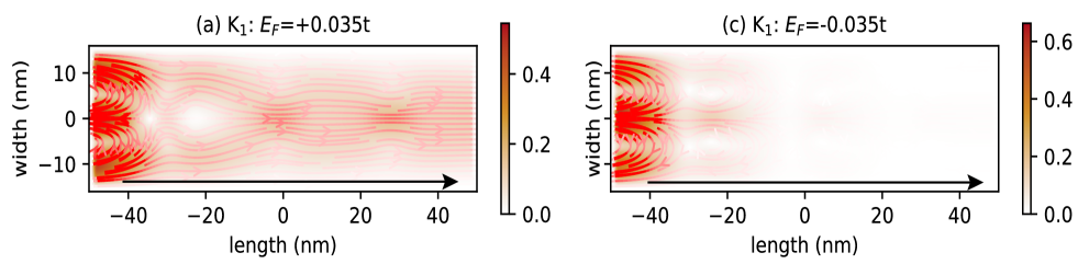
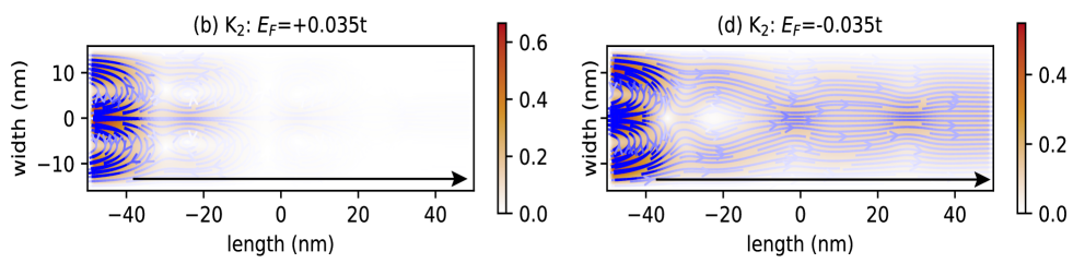
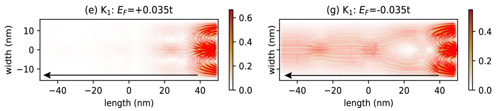
Figure 3: Local current mapping, within the gap regions ( $\lambda_{I}^{(A)}=-\lambda_{I}^{(B)}=0.025t$ ) shown in Fig. 2 (c) and (d), for both valleys for a given bias voltage while panels (e) to (h) show results for opposite biases. The left (right) panels are for positive (negative) values of $E_{F}$ . Black arrows indicate the direction of the bias-incident current. Red and blue solid lines indicate the direction of corresponding current flows.
The above observations raise the question of the inter-dot spacing $d$ ’s influence on the valley-transmission output. We have proposed that the valley-scattering processes for complete transmission occur in the presence of effective inter-dot hopping between neighboring IQDs. To test this hypothesis, we analyze the role of $d$ on the valley transmittance. As shown in Fig. 2 (e), the inter-dot hopping is present with an inter-dot space $d≥ 5r_{0}$ . We observe non-stable transmission signatures if $d≤ 5r_{0}$ . In this regime, the edges of the IQDs are closer to each other, and the transmittance peaks show values less (more) than unity (zero) for the ${\bf K_{1}}$ ( ${\bf K_{2}}$ ) valley. These might be related to mode mixing that impedes the propagation of specific transverse modes due to edge-dot coupling. Interestingly, when the $d$ value is large enough, the valley transmittance becomes stable, represented by steady curves with a uniform local density between the dots.
Finally, we analyze the role of the staggered potential $\Delta$ on the valley-transmission output, as shown in Fig. 4. The staggered potential opens a gap, playing the role of a potential barrier. Consequently, the valley imbalance is maintained for all values of $E_{F}<\Delta$ . However, the valley polarization is rapidly destroyed when $E_{F}≥\Delta$ . When the confining potential of the IQD is bigger than the incident energy, the current is completely blocked, and only resonant states from each valley ${\bf K_{1}}$ $({\bf K_{2}})$ are allowed to transmit current. In this context, the choice of incident energy must consider the strength of the IQD confinement potential.
Fig. 4 (b) and (d) show that the conductance is non-zero only for particular resonances where scatterings occur at specific values of the ISOCs and energies suited by edge-dot coupling [43, 44]. In this context, the heterostructures of graphene and hBN would exhibit this regime since, in this system, the confinement potential $\Delta$ is significant [45] and therefore, its influence on the valley filtering process would have a negative impact.
The results discussed in Fig. 4 are essential since they allow us to establish a criterion for defining the best materials for islands. Indeed, for a better response, it is necessary to use a material that provides a weak or zero confinement potential. If so, the IQDs will operate efficiently, and the overall system might be used to monitor valley-driven current by either tuning the ISOC or the RSOC. The question we might ask then is which materials are better suited for this response. Such a case would be materialized in heterostructures of twisted graphene and monolayers of transition-metal dichalcogenides (TMDCs). In such scenarios, the twisting angle substantially decreases the confinement potential, and the dominant parameters will be the valley-Zeeman and RSOCs [35]. A concrete example of a realistic proximity effect is discussed later on.
An alternative description of these effects is by considering the area around the IQDs with wider staggered potentials as an electron/hole bilayer system where the electrons are essentially required to overcome an offset barrier to be scattered through. This action is analogous to the massless-massive electron-hole system in a transverse electric field in graphene on a TMD substrate. In this context, the value of the Rashba coupling has a direct effect since it impacts the offset barrier. Due to its complexity, we postpone the study of these effects for future work. (For more details, see Refs. [29] and [28].)
<details>
<summary>x10.png Details</summary>
### Visual Description
# Technical Data Extraction: Conductance (G) vs. Spin-Orbit Coupling ($\lambda_I/t$)
This document provides a comprehensive extraction of data and trends from the provided scientific plots. The image consists of two side-by-side panels, (a) and (b), showing the conductance $G$ as a function of the dimensionless parameter $\lambda_I/t$ for different values of $\Delta$.
## 1. Global Metadata and Axis Definitions
* **Common Parameters (Both Panels):**
* $\lambda_R = 10 \text{ (meV)}$
* $E_F = 35 \text{ (meV)}$
* **Y-Axis:** Conductance $G$ in units of $(e^2/h)$.
* **Range:** 0 to 4.
* **Major Tick Marks:** 0, 1, 2, 3, 4.
* **X-Axis:** Dimensionless parameter $\lambda_I/t$.
* **Range:** 0.000 to 0.150.
* **Major Tick Marks:** 0.000, 0.025, 0.050, 0.075, 0.100, 0.125, 0.150.
* **Internal Labels:** Both panels contain two distinct regions labeled $K_1$ (upper half, $G > 2$) and $K_2$ (lower half, $G < 2$).
---
## 2. Panel (a) Analysis
**Header:** (a) $\lambda_R=10 \text{ (meV)}, E_F=35 \text{ (meV)}$
### Legend and Series Identification
* **Location:** Top right quadrant of panel (a).
* **Series 1 (Black Line):** $\Delta = 0 \text{ (meV)}$
* **Series 2 (Blue Line):** $\Delta = 5 \text{ (meV)}$
### Trend Description and Data Points
Panel (a) shows high conductance plateaus interspersed with deep gaps where conductance drops to zero.
* **Region $K_1$ (Top):**
* **Trend:** Starts at $G=4$ at $\lambda_I/t = 0$. Both lines show a plateau until $\sim 0.010$, followed by a sharp drop to $G=2$ (the floor of the $K_1$ region).
* **Plateau 1 ($\sim 0.050$ to $0.065$):** Black line reaches $G=3$. Blue line is slightly lower with oscillations.
* **Plateau 2 ($\sim 0.100$ to $0.115$):** Black line reaches $G=3$. Blue line shows a significant dip in the middle of this range.
* **Plateau 3 ($\sim 0.130$ to $0.140$):** Black line reaches $G=3$. Blue line reaches $\sim 2.5$.
* **Region $K_2$ (Bottom):**
* **Trend:** Mirrors the $K_1$ behavior but shifted down by 2 units. Starts at $G=2$.
* **Gaps:** Conductance drops to $G=0$ between $0.015-0.045$, $0.070-0.095$, and $0.115-0.125$.
* **Effect of $\Delta$:** Increasing $\Delta$ from 0 to 5 meV (Blue line) generally suppresses the conductance peaks and introduces more oscillatory behavior within the plateaus.
---
## 3. Panel (b) Analysis
**Header:** (b) $\lambda_R=10 \text{ (meV)}, E_F=35 \text{ (meV)}$
### Legend and Series Identification
* **Location:** Top right quadrant of panel (b).
* **Series 3 (Green Line):** $\Delta = 40 \text{ (meV)}$
* **Series 4 (Magenta Line):** $\Delta = 50 \text{ (meV)}$
### Trend Description and Data Points
Panel (b) shows a "suppressed" state. The $K_1$ region (top half) is entirely empty ($G=0$). All activity is confined to the $K_2$ region (bottom half) and consists of sharp, narrow spikes rather than broad plateaus.
* **Region $K_1$ (Top):**
* **Trend:** Constant $G=0$ for both series across the entire x-axis range.
* **Region $K_2$ (Bottom):**
* **Series 3 (Green):** Shows clusters of sharp spikes.
* Cluster 1: $\sim 0.020 - 0.025$, peak $G \approx 1.6$.
* Cluster 2: $\sim 0.055 - 0.065$, peak $G \approx 1.4$.
* Cluster 3: $\sim 0.105 - 0.110$, peak $G \approx 1.3$.
* Cluster 4: $\sim 0.145 - 0.150$, peak $G \approx 1.3$.
* **Series 4 (Magenta):** Shows even fewer and narrower spikes.
* Spike 1: $\sim 0.035$, very low $G$.
* Spike 2: $\sim 0.065$, $G \approx 0.5$.
* Spike 3: $\sim 0.075$, $G \approx 0.5$.
* Spike 4: $\sim 0.100$, $G \approx 1.3$.
* Spike 5: $\sim 0.115$, $G \approx 1.4$.
* Spike 6: $\sim 0.120$, $G \approx 0.7$.
---
## 4. Summary of Observations
1. **Phase Transition:** There is a clear transition between panel (a) and (b). Low $\Delta$ (0-5 meV) allows for broad conductance plateaus and transport in both $K_1$ and $K_2$ regimes. High $\Delta$ (40-50 meV) destroys the $K_1$ transport and reduces $K_2$ transport to isolated resonance spikes.
2. **Symmetry:** The $K_1$ and $K_2$ regions in panel (a) are mathematically related by a vertical shift of 2 units ($G_{K1} = G_{K2} + 2$).
3. **Impact of $\Delta$:** Increasing the $\Delta$ parameter acts as a gap-opening mechanism that suppresses the total conductance and eventually localizes the transport into narrow energy/coupling windows.
</details>
<details>
<summary>x11.png Details</summary>
### Visual Description
# Technical Data Extraction: Conductance Plots (c) and (d)
This document provides a detailed extraction of the data and components from two scientific line charts representing conductance ($G$) as a function of a dimensionless parameter ($\lambda_I/t$).
## 1. Global Metadata and Axis Definitions
The image consists of two side-by-side panels, labeled **(c)** and **(d)**. Both panels share the same physical dimensions and axis scales.
* **X-Axis (Horizontal):**
* **Label:** $\lambda_I/t$
* **Range:** $0.000$ to $0.150$
* **Major Tick Intervals:** $0.025$
* **Y-Axis (Vertical):**
* **Label:** $G$ ($e^2/h$)
* **Range:** $0$ to $4$
* **Major Tick Intervals:** $1$
* **Common Parameters (Header):**
* $\lambda_R = 15$ (meV)
* $E_F = -35$ (meV)
* **Internal Region Labels:** Both charts contain boxed labels $K_1$ and $K_2$.
* $K_1$ is positioned in the lower half of the plot (near $G \approx 1$ to $2$).
* $K_2$ is positioned in the upper half of the plot (near $G \approx 3$ to $4$).
---
## 2. Panel (c) Analysis
### Legend and Series Identification
* **Location:** Top right quadrant.
* **Series 1 (Black Line):** $\Delta = 0$ (meV).
* **Series 2 (Blue Line):** $\Delta = 5$ (meV).
### Trend Description
Panel (c) shows quantized conductance plateaus. The black line ($\Delta=0$) generally forms the upper envelope of the data, while the blue line ($\Delta=5$) shows suppressed conductance in specific regions. The data is split into two distinct bands: a lower band centered around $K_1$ and an upper band centered around $K_2$.
### Data Points and Features
* **Initial State ($\lambda_I/t = 0$):** Conductance starts at maximum values ($G=2$ for $K_1$, $G=4$ for $K_2$).
* **First Drop:** Both series drop sharply to $G=0$ at approximately $\lambda_I/t \approx 0.015$.
* **Plateau 1 ($\lambda_I/t \approx 0.050$ to $0.065$):**
* **Black Line:** Reaches a stable plateau at $G=1$ (for $K_1$) and $G=3$ (for $K_2$).
* **Blue Line:** Shows a slight dip/oscillation, staying slightly below the black line.
* **Plateau 2 ($\lambda_I/t \approx 0.100$ to $0.115$):**
* **Black Line:** Returns to $G=1$ and $G=3$ plateaus.
* **Blue Line:** Shows significant suppression compared to the black line, dipping toward $G \approx 0.6$ (for $K_1$) and $G \approx 2.6$ (for $K_2$).
* **Plateau 3 ($\lambda_I/t \approx 0.130$ to $0.145$):**
* **Black Line:** Returns to $G=1$ and $G=3$ plateaus.
* **Blue Line:** Again shows suppression and oscillations below the black line.
---
## 3. Panel (d) Analysis
### Legend and Series Identification
* **Location:** Top right quadrant.
* **Series 1 (Green Line):** $\Delta = 40$ (meV).
* **Series 2 (Magenta Line):** $\Delta = 50$ (meV).
### Trend Description
Unlike panel (c), panel (d) shows almost zero conductance across most of the range, with the exception of sharp, narrow "spikes" or resonance peaks. The $K_2$ region (upper half) is entirely empty (conductance is zero). All activity occurs in the $K_1$ region.
### Data Points and Features
* **Baseline:** Both series are at $G=0$ for the majority of the x-axis.
* **Green Series ($\Delta=40$):**
* **Cluster 1:** Sharp spikes between $\lambda_I/t \approx 0.020$ and $0.025$, reaching heights up to $G \approx 1.6$.
* **Cluster 2:** Spikes near $\lambda_I/t \approx 0.055$ and $0.065$, reaching $G \approx 1.3$.
* **Cluster 3:** Spikes near $\lambda_I/t \approx 0.105$, reaching $G \approx 1.3$.
* **Cluster 4:** Spikes near the end of the scale $\lambda_I/t \approx 0.145$.
* **Magenta Series ($\Delta=50$):**
* Shows much fewer and narrower peaks than the green series.
* Notable peaks at $\lambda_I/t \approx 0.035$ (very low), $0.068$, $0.075$, $0.100$, $0.115$ (highest magenta peak at $G \approx 1.4$), and $0.120$.
---
## 4. Comparative Summary
| Feature | Panel (c) | Panel (d) |
| :--- | :--- | :--- |
| **$\Delta$ Values** | Low (0, 5 meV) | High (40, 50 meV) |
| **Conductance Profile** | Broad plateaus and gaps | Sparse, sharp resonance peaks |
| **$K_2$ Activity** | High ($G$ up to 4) | Zero ($G = 0$) |
| **$K_1$ Activity** | High ($G$ up to 2) | Sparse spikes ($G$ up to ~1.6) |
**Conclusion:** Increasing the parameter $\Delta$ from the values in (c) to those in (d) causes a transition from a regime of quantized plateau conductance to a regime of suppressed conductance characterized by isolated resonance tunneling peaks, specifically quenching all transport in the $K_2$ channel.
</details>
Figure 4: Valley conductance vs intrinsic spin-orbit length $\lambda_{I}$ for different values of staggered potential $\Delta$ . The left (right) panels correspond to $\Delta<E_{F}$ ( $\Delta>E_{F}$ ).
III.1.3 Valley-Hall and bulk conductivities
We briefly discuss the emergence of Hall and bulk conductivities in these structures. We visualize the origin of these conductivities by mapping the local current flow and highlighting the valley polarization with solid blue (red) curves indicating the ${\bf K_{1}}$ ( ${\bf K_{2}}$ ) index in Fig. 5. Analysis of the figure reveals that the generated valley currents are composed of bulk-driven and Hall-driven currents. In this process, the local current where both valleys are scattered shows that each valley is conducting with either bulk or Hall currents depending on the sign of the Fermi energy. This analysis suggests that a periodic array of dots with the best choice of SOCs offers an alternative mechanism for generating valley-neutral Hall currents since both valleys contribute to the current in the same direction, although through different regions. A realistic example is discussed in Sec. III.3 where we find induced SOC terms that facilitate valley-Hall current for a given TMDs island and twist angle.
<details>
<summary>x12.png Details</summary>
### Visual Description
# Technical Data Extraction: Current Density Streamline Plots
This image contains two side-by-side scientific plots (labeled 'a' and 'c') representing current density streamlines in a nanostructure. The plots visualize the flow of current through a channel of varying width or potential.
## 1. Global Metadata
* **Language:** English
* **X-Axis Label (both plots):** `length (nm)`
* **X-Axis Scale:** -40 to 40 (with ticks at -40, -20, 0, 20, 40)
* **Y-Axis Label (both plots):** `width (nm)`
* **Y-Axis Scale:** -10 to 10 (with ticks at -10, 0, 10)
* **Color Scale:** Sequential heatmap (White $\rightarrow$ Light Orange $\rightarrow$ Dark Red).
* **Visual Elements:** Red streamlines with directional arrows pointing generally from left to right. A black horizontal arrow at the bottom of each plot indicates the primary direction of flow.
---
## 2. Component Analysis
### Plot (a): $K_1: E_F = +0.035t$
* **Header Text:** `(a) K₁: E_F=+0.035t`
* **Color Bar Range:** 0.0 to ~0.35 (Ticks at 0.0, 0.1, 0.2, 0.3)
* **Spatial Grounding [x, y]:** The color bar is located to the right of the plot.
* **Trend Description:** The current density is high (dark red) and widely distributed across the width of the channel. The streamlines show a "pinched" behavior at regular intervals along the length (approximately at $x = -35, -5, 25$ nm).
* **Key Observations:**
* The flow is robust across the entire width (-10 to 10 nm).
* There are distinct "bubbles" or regions of lower density (white/light orange) centered at $y=0$ between the pinch points.
* The streamlines are densest (darkest red) near the edges of these central bubbles.
### Plot (c): $K_1: E_F = -0.035t$
* **Header Text:** `(c) K₁: E_F=-0.035t`
* **Color Bar Range:** 0.0 to ~0.45 (Ticks at 0.0, 0.2, 0.4)
* **Spatial Grounding [x, y]:** The color bar is located to the right of the plot.
* **Trend Description:** Compared to plot (a), the current density is significantly more concentrated along the horizontal center line ($y=0$). The intensity (darkness of red) is higher in the central core but drops off much faster toward the edges ($y = \pm 10$).
* **Key Observations:**
* The flow is "collimated" or focused toward the center.
* The pinch points are still visible but appear more as nodes in a narrow beam rather than the wide-channel oscillations seen in plot (a).
* The regions near the top and bottom boundaries ($y > 5$ and $y < -5$) show very low current density (white).
---
## 3. Comparative Summary
| Feature | Plot (a) | Plot (c) |
| :--- | :--- | :--- |
| **Fermi Energy ($E_F$)** | $+0.035t$ (Positive) | $-0.035t$ (Negative) |
| **Max Intensity** | ~0.35 | ~0.45 |
| **Flow Distribution** | Wide; fills the 20nm width. | Narrow; concentrated at the center. |
| **Pattern** | Oscillatory wide-channel flow. | Focused beam-like flow with nodes. |
**Technical Conclusion:** The sign of the Fermi energy ($E_F$) dictates the spatial distribution of the current. A positive $E_F$ results in a more spread-out current density across the nanostructure's width, while a negative $E_F$ of the same magnitude causes the current to focus into a narrow central beam.
</details>
<details>
<summary>x13.png Details</summary>
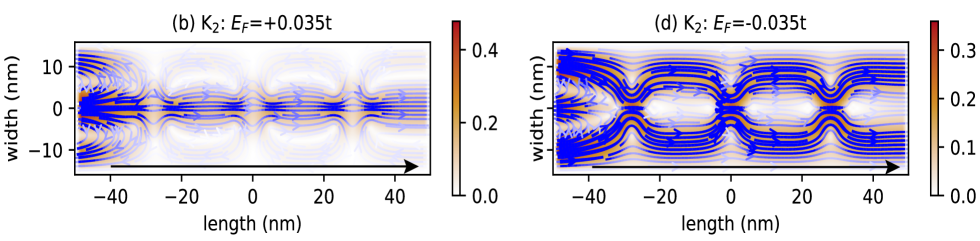
### Visual Description
# Technical Data Extraction: Current Density and Flow Streamlines
This image consists of two side-by-side scientific plots (labeled **b** and **d**) representing physical simulations of current flow in a nanostructure. The plots utilize heatmaps to show magnitude and blue streamlines with arrows to indicate the direction and density of flow.
---
## 1. Component Isolation: Plot (b)
### Header Information
* **Label:** (b)
* **Title:** $K_2: E_F = +0.035t$
* **Physical Context:** Represents a state with positive Fermi energy ($E_F$).
### Axis and Scale
* **Y-axis (Left):** labeled "width (nm)". Scale markers at -10, 0, 10.
* **X-axis (Bottom):** labeled "length (nm)". Scale markers at -40, -20, 0, 20, 40.
* **Color Bar (Right):** Vertical scale representing magnitude.
* **Range:** 0.0 to 0.4 (units unspecified, likely normalized current density).
* **Color Gradient:** White (0.0) $\rightarrow$ Light Orange $\rightarrow$ Dark Brown/Rust (0.4).
### Data Trends and Flow Analysis
* **Spatial Distribution:** The highest intensity (darkest orange) is concentrated along the central horizontal axis (width = 0) and at the far left entrance.
* **Flow Pattern:** Blue streamlines originate from the left ($x \approx -50$) and move toward the right.
* **Trend Verification:** The flow is highly collimated along the center. There are periodic "nodes" or narrowing points along the center line at approximately $x = -30, -5, 20,$ and $45$.
* **Peripheral Activity:** Outside the central channel, the streamlines form faint, recirculating vortices or "eddies" in the regions where the heatmap is white/light (low magnitude).
---
## 2. Component Isolation: Plot (d)
### Header Information
* **Label:** (d)
* **Title:** $K_2: E_F = -0.035t$
* **Physical Context:** Represents a state with negative Fermi energy ($E_F$).
### Axis and Scale
* **Y-axis (Left):** labeled "width (nm)". Scale markers at -10, 0, 10.
* **X-axis (Bottom):** labeled "length (nm)". Scale markers at -40, -20, 0, 20, 40.
* **Color Bar (Right):** Vertical scale representing magnitude.
* **Range:** 0.0 to 0.3 (Note: The peak scale is lower than plot b).
* **Color Gradient:** White (0.0) $\rightarrow$ Light Orange $\rightarrow$ Dark Brown/Rust (0.3).
### Data Trends and Flow Analysis
* **Spatial Distribution:** Unlike plot (b), the high-intensity regions (orange) are split into two parallel channels above and below the center line, roughly at width $\approx \pm 5$ nm. The center line (width = 0) shows low intensity (white).
* **Flow Pattern:** Blue streamlines are much denser and more widespread than in plot (b).
* **Trend Verification:** The streamlines exhibit a "braided" or "cellular" appearance. They diverge from the center at the entrance and follow the two outer paths, periodically pinching inward at $x \approx -25, 0, 25$.
* **Comparison:** This plot shows a clear "hollow" center in terms of current density magnitude compared to the "solid" center in plot (b).
---
## 3. Summary Table of Extracted Labels
| Feature | Plot (b) | Plot (d) |
| :--- | :--- | :--- |
| **Fermi Energy ($E_F$)** | $+0.035t$ | $-0.035t$ |
| **Max Scale Value** | 0.4 | 0.3 |
| **Primary Flow Path** | Central (width = 0) | Bifurcated (width $\approx \pm 5$) |
| **X-axis Range** | -50 to 50 nm | -50 to 50 nm |
| **Y-axis Range** | -15 to 15 nm | -15 to 15 nm |
## 4. Embedded Annotations
* **Directional Arrows:** Both plots contain a long black arrow at the bottom pointing from left to right, explicitly indicating the global direction of transport/length.
* **Streamline Arrows:** Small blue arrowheads are embedded within the blue lines to show local vector direction. In both plots, the net flow is from left to right, though local curvatures exist.
</details>
<details>
<summary>x14.png Details</summary>
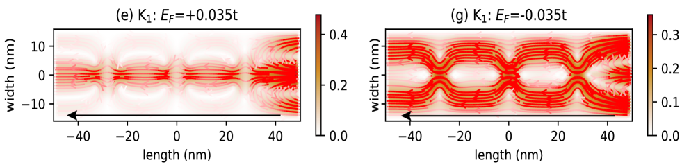
### Visual Description
# Technical Data Extraction: Current Density Streamline Plots
This document provides a detailed extraction of the data and components from the provided image, which consists of two side-by-side scientific plots (labeled 'e' and 'g') representing current density distributions in a nanostructure.
## 1. Global Image Metadata
* **Language:** English
* **Subject Matter:** Physics/Nanotechnology (likely Graphene or 2D materials research).
* **Visual Format:** Heatmaps with overlaid vector streamlines.
* **Coordinate System:** Cartesian coordinates representing physical dimensions in nanometers (nm).
---
## 2. Component Isolation: Plot (e)
### Header Information
* **Label:** (e)
* **Title String:** $K_1: E_F = +0.035t$
* **Interpretation:** This represents the $K_1$ valley with a positive Fermi energy ($E_F$) of $0.035t$.
### Axis and Scale
* **Y-axis Label:** width (nm)
* **Y-axis Markers:** -10, 0, 10
* **X-axis Label:** length (nm)
* **X-axis Markers:** -40, -20, 0, 20, 40
* **Color Bar (Legend):** Located at the right of the plot.
* **Scale:** 0.0 to 0.4 (units unspecified, likely normalized current density).
* **Color Gradient:** White (0.0) $\rightarrow$ Light Orange $\rightarrow$ Dark Red/Brown (0.4).
### Data Trends and Flow
* **Spatial Grounding:** The current is concentrated primarily along the central horizontal axis ($y = 0$).
* **Flow Direction:** Indicated by a black arrow at the bottom pointing from right to left (from $+50$ nm toward $-50$ nm).
* **Visual Trend:** The current density shows a "pinched" or "focused" behavior. There are four distinct high-intensity nodes (darker orange/red) located along the center line at approximately $x = -35, -10, +15,$ and $+40$ nm.
* **Streamline Behavior:** Red streamlines are tightly packed in the center, indicating a collimated flow of current through the middle of the channel.
---
## 3. Component Isolation: Plot (g)
### Header Information
* **Label:** (g)
* **Title String:** $K_1: E_F = -0.035t$
* **Interpretation:** This represents the $K_1$ valley with a negative Fermi energy ($E_F$) of $-0.035t$.
### Axis and Scale
* **Y-axis Label:** width (nm)
* **Y-axis Markers:** -10, 0, 10
* **X-axis Label:** length (nm)
* **X-axis Markers:** -40, -20, 0, 20, 40
* **Color Bar (Legend):** Located at the right of the plot.
* **Scale:** 0.0 to 0.3 (Note: The maximum scale is lower than plot 'e').
* **Color Gradient:** White (0.0) $\rightarrow$ Light Orange $\rightarrow$ Dark Red/Brown (0.3).
### Data Trends and Flow
* **Spatial Grounding:** Unlike plot (e), the current density is concentrated along the **edges** of the channel (near $y = 10$ and $y = -10$).
* **Flow Direction:** Indicated by a black arrow at the bottom pointing from right to left.
* **Visual Trend:** The center of the channel ($y = 0$) is largely white (low density), while the current flows in "wavy" or "snaking" patterns along the top and bottom boundaries.
* **Streamline Behavior:** The red streamlines are bifurcated. They move away from the center and hug the edges, showing periodic oscillations or "bumps" that correspond to the same $x$-positions as the nodes in plot (e).
---
## 4. Comparative Analysis Summary
| Feature | Plot (e) | Plot (g) |
| :--- | :--- | :--- |
| **Fermi Energy ($E_F$)** | $+0.035t$ (Positive) | $-0.035t$ (Negative) |
| **Max Intensity** | ~0.4 | ~0.3 |
| **Current Path** | Central/Axial flow | Edge/Boundary flow |
| **Flow Direction** | Right to Left | Right to Left |
| **Pattern Type** | Focused nodes in center | Oscillatory paths along edges |
**Conclusion:** The transition from positive to negative Fermi energy causes a spatial shift in current transport from the bulk/center of the nanostructure to the edges, a phenomenon often associated with topological insulators or specific edge states in 2D materials.
</details>
<details>
<summary>x15.png Details</summary>
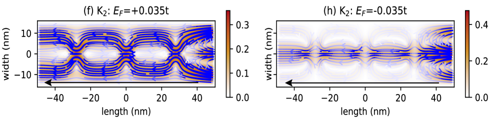
### Visual Description
# Technical Data Extraction: Streamline and Heatmap Analysis
This document provides a detailed technical extraction of the provided image, which consists of two side-by-side scientific plots (labeled 'f' and 'h') representing physical simulations, likely related to electron flow or current density in a nanostructure.
## 1. Global Metadata
* **Language:** English
* **Primary Components:** Two subplots with heatmaps, streamline overlays, and color bars.
* **X-Axis (Common):** `length (nm)` ranging from approximately -50 to 50.
* **Y-Axis (Common):** `width (nm)` ranging from -15 to 15.
* **Directional Indicator:** A black arrow at the bottom of both plots points from right to left (from +40 to -45 on the x-axis).
---
## 2. Subplot (f) Analysis
### Header Information
* **Label:** (f)
* **Title:** $K_2: E_F = +0.035t$
### Axis and Scale
* **X-axis Markers:** -40, -20, 0, 20, 40
* **Y-axis Markers:** -10, 0, 10
* **Color Bar Range:** 0.0 to 0.3 (linear scale).
* **Color Bar Gradient:** Light beige/white (0.0) to dark orange/brown (0.3).
### Data Visualization (Heatmap & Streamlines)
* **Heatmap Trend:** The highest intensity (dark orange, ~0.3) is concentrated in horizontal bands along the top and bottom edges (approx. $y = \pm 10$ nm) and in "bottleneck" regions between circular voids.
* **Streamline Behavior:**
* Blue lines with arrows indicate flow direction.
* The flow enters from the right and moves toward the left.
* The streamlines form four distinct "cells" or vortices centered along the $y=0$ axis at roughly $x = -30, -10, 10, 30$.
* The flow is most compressed and intense (darker blue) at the narrow passages between these cells.
* **Spatial Features:** There are four low-intensity (white) circular regions centered at $y=0$, suggesting areas of zero or near-zero magnitude.
---
## 3. Subplot (h) Analysis
### Header Information
* **Label:** (h)
* **Title:** $K_2: E_F = -0.035t$
### Axis and Scale
* **X-axis Markers:** -40, -20, 0, 20, 40
* **Y-axis Markers:** -10, 0, 10
* **Color Bar Range:** 0.0 to 0.4 (linear scale). Note: This scale is higher than subplot (f).
* **Color Bar Gradient:** Light beige/white (0.0) to dark orange/brown (0.4).
### Data Visualization (Heatmap & Streamlines)
* **Heatmap Trend:** Compared to (f), the intensity is much more concentrated along the central horizontal axis ($y=0$). The edges of the channel (top and bottom) show very low intensity (white).
* **Streamline Behavior:**
* Blue lines with arrows indicate flow from right to left.
* The flow is highly collimated along the center of the channel.
* While there are subtle "pinching" effects at the same x-coordinates as subplot (f) ($x \approx \pm 10, \pm 30$), the streamlines do not form the wide, expansive loops seen in the previous plot.
* The flow appears "squeezed" into a narrow central filament.
* **Spatial Features:** The high-intensity regions (dark orange) are located at the "nodes" or pinch points along the $y=0$ line.
---
## 4. Comparative Summary
| Feature | Subplot (f) | Subplot (h) |
| :--- | :--- | :--- |
| **Fermi Energy ($E_F$)** | $+0.035t$ (Positive) | $-0.035t$ (Negative) |
| **Max Intensity Value** | ~0.3 | ~0.4 |
| **Flow Distribution** | Broad, filling the width of the channel. | Narrow, concentrated along the center. |
| **Vortex/Cell Formation** | Strong, expansive cells around $y=0$. | Weak, highly compressed flow along $y=0$. |
| **Edge Intensity** | High at $y = \pm 10$ nm. | Low at $y = \pm 10$ nm. |
**Conclusion:** The change in the sign of the Fermi energy ($E_F$) from positive to negative causes a dramatic shift in the spatial distribution of the flow, moving it from the edges and wide cells (f) to a highly concentrated central stream (h).
</details>
Figure 5: Local valley polarized currents at ${\bf K_{1}}$ and ${\bf K_{2}}$ valleys, in the presence of only staggered intrinsic SOC, $\lambda_{I}^{(A)}=-\lambda_{I}^{(B)}=0.075t$ . The left (right) panels are for $E_{F}>0$ ( $E_{F}<0$ ).
III.2 Description of the model with weak couplings
A quantitative description of the model with realistic parameters requires discussing the above results for the weaker strengths of the various SOCs. An important question is how the valley-conductance is affected by changes in the RSOC values.
III.2.1 Valley-dependent conductance by tuning the Rashba coupling
In this context, we consider weaker ISOCs as expected in realistic settings and an increased and controllable strength of RSOC. We notice that IQDs refer, in reality, to any heterostructure that exhibits $C_{3v}$ -symmetry. This section considers only ISO and RSO couplings, while the pseudospin inversion asymmetry (PIA) coupling in systems with broken inversion symmetry is discussed in the following section. A typical example of such a setup would be twisted graphene/transition-metal-dichalcogenides heterostructures since the relative rotation leads to a negligible value of PIA coupling. To this end, the IQDs with $C_{3v}$ -symmetry might lead to potential applications since the Rashba coupling can be tuned using a transverse electric field. As realized, we consider weak staggered couplings $\lambda_{I}^{(A)}=-\lambda_{I}^{(B)}=0.015t$ , we inject electrons with $E_{F}=± 0.035t$ into several-identical QDs, and by shifting the Rashba coupling with the aid of top gates, we compute the valley conductance through the system.
In Fig. 6 (a) and (b), we show results for valley transmittance when the top gate is used to obtain a valley polarized conductance for coupling within the ranges $0.07t≤\lambda_{R}≤ 0.12t$ and $0.1t≤\lambda_{R}≤ 0.2t$ , for the two values of the staggered potential $\Delta=0$ anc $\Delta=0.02t$ correspondingly. The valley transmission for ${\bf K_{1}}$ , $({\bf K_{2}})$ jumps almost from 2 to 0 for positive (negative) incident energy, indicating that only electrons with either valley ${\bf K_{1}}$ or valley ${\bf K_{2}}$ go through the system.
The most important conclusion from the results is that reasonable and better control of the valley transmission can be obtained by tuning a gate bias using IQDs with weak couplings. In this context, a quantitative understanding might easily be reached. By controlling the Rashba strength, the wave function may interfere destructively or constructively depending on the valley and the sign of the incident energy. It is seen that at $E_{F}>0$ and $\lambda_{R}≥ 0.05t$ , the wave function around ${\bf K_{1}}$ is transmitted through the IQDs region, where the wave function around ${\bf K_{2}}$ vanishes (is reflected), resulting on a polarized valley transmission, invertible by changes in the sign of the incident energy.
These results can be understood from the analysis of the band structure in Fig. 6 (c) and (d). By analyzing the RSOC’s contributions to the edge state, we observe that for weak Rashba couplings, such as $\lambda_{R}=0.025t$ , the edge state is mixed with the bulk conduction bands. However, for $\lambda_{R}=0.075t$ , the system might sustain isolated and steady helical edge states, depending on the spin nature, as discussed in earlier works [29].
<details>
<summary>x16.png Details</summary>
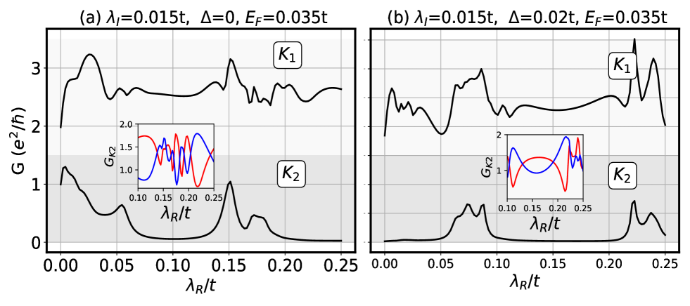
### Visual Description
# Technical Data Extraction: Conductance Plots (a) and (b)
This document provides a comprehensive extraction of the data and components from the provided image, which consists of two side-by-side line charts representing conductance ($G$) as a function of Rashba coupling ($\lambda_R/t$).
## 1. Global Metadata and Axis Definitions
* **Y-Axis (Primary):** Conductance $G$ measured in units of $(e^2/\hbar)$.
* **Scale:** 0 to 3.5.
* **Major Tick Marks:** 0, 1, 2, 3.
* **X-Axis (Primary):** Dimensionless Rashba coupling parameter $\lambda_R/t$.
* **Scale:** 0.00 to 0.25.
* **Major Tick Marks:** 0.00, 0.05, 0.10, 0.15, 0.20, 0.25.
* **Visual Features:** Both plots contain a light gray shaded horizontal band between $G \approx 0$ and $G \approx 1.5$.
---
## 2. Panel (a) Analysis
**Header Label:** (a) $\lambda_I = 0.015t, \Delta = 0, E_F = 0.035t$
### Main Plot Components
Panel (a) contains two distinct black data series labeled with boxed text.
* **Series $K_1$ (Upper Line):**
* **Trend:** Starts at $G \approx 2.0$. It shows a significant peak at $\lambda_R/t \approx 0.025$ reaching $G \approx 3.2$. It then oscillates with a general downward trend toward $G \approx 2.5$ before a sharp spike at $\lambda_R/t \approx 0.15$ (reaching $G \approx 3.1$). It ends at $G \approx 2.6$.
* **Spatial Grounding:** Label $K_1$ is located at the top right [x=0.85, y=0.90] relative to the panel.
* **Series $K_2$ (Lower Line):**
* **Trend:** Starts at $G \approx 1.0$, peaks quickly at $\lambda_R/t \approx 0.01$, then decays toward zero. It remains near zero between $0.07 < \lambda_R/t < 0.13$. It exhibits a sharp, narrow peak at $\lambda_R/t \approx 0.15$ (reaching $G \approx 1.0$) and then returns to near zero.
* **Spatial Grounding:** Label $K_2$ is located at the middle right [x=0.85, y=0.40] relative to the panel.
### Inset Plot (a)
* **Axes:** Y-axis is $G_{K2}$ (range 0.5 to 2.0); X-axis is $\lambda_R/t$ (range 0.10 to 0.25).
* **Data Series:**
* **Blue Line:** Starts low ($\approx 0.8$), rises to a peak at $\approx 0.22$, then drops.
* **Red Line:** Starts high ($\approx 1.7$), drops to a minimum at $\approx 0.22$, then rises.
* **Observation:** The blue and red lines show an anti-correlated oscillatory behavior.
---
## 3. Panel (b) Analysis
**Header Label:** (b) $\lambda_I = 0.015t, \Delta = 0.02t, E_F = 0.035t$
*Note: The introduction of $\Delta = 0.02t$ is the primary variable change from panel (a).*
### Main Plot Components
* **Series $K_1$ (Upper Line):**
* **Trend:** Starts at $G \approx 1.8$. It shows a series of small oscillations between $0.00 < \lambda_R/t < 0.05$, a dip at $0.05$, and a broad plateau around $G \approx 2.3$. A very sharp, high-amplitude double peak occurs between $0.20 < \lambda_R/t < 0.25$, with the highest point reaching $G \approx 3.5$.
* **Spatial Grounding:** Label $K_1$ is located at [x=0.85, y=0.85].
* **Series $K_2$ (Lower Line):**
* **Trend:** Remains at $G \approx 0$ for the majority of the range. It shows a small double-hump feature between $0.06 < \lambda_R/t < 0.10$ (max $G \approx 0.7$). It returns to zero and then shows a final sharp peak at $\lambda_R/t \approx 0.22$ (max $G \approx 0.8$).
* **Spatial Grounding:** Label $K_2$ is located at [x=0.85, y=0.40].
### Inset Plot (b)
* **Axes:** Y-axis is $G_{K2}$ (range 0 to 2); X-axis is $\lambda_R/t$ (range 0.10 to 0.25).
* **Data Series:**
* **Blue Line:** Shows a "W" shape; peaks at $0.11$ and $0.22$, with a local minimum in the center.
* **Red Line:** Shows an "M" shape; peaks in the center ($\lambda_R/t \approx 0.17$) and has deep minima at $0.11$ and $0.22$.
* **Observation:** These lines are perfectly out of phase (anti-correlated).
---
## 4. Summary of Key Trends
1. **Effect of $\Delta$:** Comparing (a) to (b), the introduction of a non-zero $\Delta$ suppresses the conductance of $K_2$ across most of the $\lambda_R/t$ range, except for specific resonance peaks.
2. **Resonance:** Both plots show sharp conductance spikes at high $\lambda_R/t$ values (around 0.15 for $\Delta=0$ and around 0.22 for $\Delta=0.02t$).
3. **Symmetry in Insets:** The insets reveal that while the total conductance might fluctuate, the sub-components (Red and Blue lines) maintain a reciprocal relationship, where the increase in one corresponds to the decrease in the other.
</details>
<details>
<summary>x17.png Details</summary>

### Visual Description
# Technical Data Extraction: Electronic Band Structure Plots
This document provides a detailed technical extraction of the information contained in the provided image, which consists of two side-by-side electronic band structure plots (labeled 'c' and 'd').
## 1. General Metadata and Axis Information
The image displays two subplots representing energy ($E$) versus wavevector ($k$).
* **Vertical Axis (Y-axis):**
* **Label:** $E \text{ (eV)}$
* **Range:** $-0.4$ to $0.4$
* **Major Tick Marks:** $-0.4, -0.2, 0.0, 0.2, 0.4$
* **Horizontal Axis (X-axis):**
* **Label:** $k [\pi/a]$
* **Range:** Approximately $-4.4$ to $-1.8$
* **Major Tick Marks:** $-4.0, -3.5, -3.0, -2.5, -2.0$
* **Grid:** Both plots feature a light gray rectangular grid aligned with the major tick marks.
---
## 2. Subplot (c) Analysis
### Header Information
* **Label:** (c)
* **Parameters:** $\lambda_I^{(A)} = -\lambda_I^{(B)}, \lambda_R = 0.025t$
### Component Isolation and Trends
Subplot (c) shows a band structure with a distinct bulk gap and topological edge states.
* **Bulk Bands (Dense regions):**
* Located primarily around $k \approx -3.9$ and $k \approx -2.4$.
* **Trend:** These bands form "V" shapes (conduction bands) and inverted "V" shapes (valence bands) that converge toward $E = 0$ but remain separated by a small energy gap.
* The bands are multi-colored, indicating a manifold of states.
* **Edge States (Crossing lines):**
* Four distinct linear bands cross the gap between the bulk manifolds.
* **Purple Line:** Slopes upward from left to right, crossing $E=0$ at $k \approx -3.2$.
* **Brown Line:** Slopes downward from left to right, crossing $E=0$ at $k \approx -3.2$.
* **Red Line:** Slopes downward from left to right, crossing $E=0$ at $k \approx -2.8$.
* **Green Line:** Slopes upward from left to right, crossing $E=0$ at $k \approx -2.8$.
* **Gap Characteristics:**
* The bulk gap is centered at $E = 0$.
* The crossing points of the edge states (Dirac points) are located exactly at $E = 0$ for $k \approx -3.2$ and $k \approx -2.8$.
---
## 3. Subplot (d) Analysis
### Header Information
* **Label:** (d)
* **Parameters:** $\lambda_I^{(A)} = -\lambda_I^{(B)}, \lambda_R = 0.075t$
### Component Isolation and Trends
Subplot (d) shows the effect of increasing the $\lambda_R$ parameter compared to plot (c).
* **Bulk Bands:**
* The bulk bands around $k \approx -3.9$ and $k \approx -2.4$ appear more "squashed" or flattened compared to plot (c).
* **Trend:** There is a noticeable oscillation or "wavy" pattern introduced in the bands near the gap edges, particularly visible between $k = -4.4$ and $-4.0$.
* **Edge States (Crossing lines):**
* The same four colored lines (Purple, Brown, Red, Green) are present.
* **Trend:** While they still cross the gap, their slopes are modified.
* **Purple/Brown crossing:** Shifted slightly. The crossing point remains near $E=0$ but the lines show slight curvature as they approach the bulk bands.
* **Red/Green crossing:** Similar to the other pair, they maintain a crossing near $E=0$ at $k \approx -2.8$.
* **Gap Characteristics:**
* The global energy gap between the bulk valence and conduction bands appears smaller than in plot (c) due to the increased $\lambda_R$ value causing the bands to push closer to the Fermi level ($E=0$).
---
## 4. Comparative Summary
| Feature | Subplot (c) [$\lambda_R = 0.025t$] | Subplot (d) [$\lambda_R = 0.075t$] |
| :--- | :--- | :--- |
| **Bulk Band Shape** | Sharp "V" and inverted "V" | Flattened and oscillatory/wavy |
| **Bulk Gap Size** | Larger | Smaller |
| **Edge States** | Linear crossings at $E=0$ | Crossings at $E=0$ with increased curvature |
| **Symmetry** | Highly symmetric around $E=0$ | Maintains particle-hole symmetry |
**Conclusion:** The increase in the $\lambda_R$ parameter from $0.025t$ to $0.075t$ results in a narrowing of the bulk bandgap and the introduction of more complex dispersion (oscillations) in the bulk energy bands, while preserving the topological edge state crossings at the Fermi level.
</details>
<details>
<summary>x18.png Details</summary>
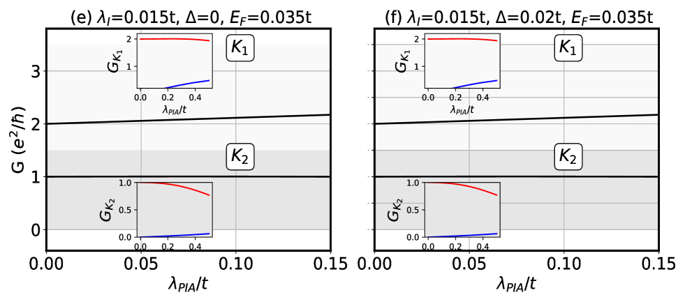
### Visual Description
# Technical Data Extraction: Conductance Plots (e) and (f)
This document provides a detailed technical extraction of the data and components from the provided image, which contains two side-by-side scientific plots labeled **(e)** and **(f)**. These plots illustrate the relationship between conductance ($G$) and the parameter $\lambda_{PIA}/t$.
---
## 1. Global Metadata and Axis Definitions
* **Primary Y-Axis (Main Plots):** Conductance $G$ in units of $(e^2/\hbar)$.
* **Scale:** Linear, ranging from $0$ to approximately $3.5$.
* **Major Ticks:** $0, 1, 2, 3$.
* **Primary X-Axis (Main Plots):** Dimensionless parameter $\lambda_{PIA}/t$.
* **Scale:** Linear, ranging from $0.00$ to $0.15$.
* **Major Ticks:** $0.00, 0.05, 0.10, 0.15$.
* **Spatial Regions:** Each plot is divided into horizontal shaded regions.
* **Region $K_1$:** Upper region (white/light background), centered around $G \approx 2$.
* **Region $K_2$:** Lower region (grey shaded background), centered around $G \approx 1$.
---
## 2. Plot (e) Analysis
**Header Parameters:** $\lambda_I = 0.015t, \Delta = 0, E_F = 0.035t$
### Main Chart Trends
* **Upper Line (Region $K_1$):** Starts at $G = 2.0$ when $\lambda_{PIA}/t = 0$. It exhibits a slight positive linear slope, reaching approximately $G \approx 2.2$ at $\lambda_{PIA}/t = 0.15$.
* **Lower Line (Region $K_2$):** Remains perfectly flat (constant) at $G = 1.0$ across the entire x-axis range.
### Inset Plots (Sub-components)
* **Top Inset ($G_{K_1}$ vs $\lambda_{PIA}/t$):**
* **X-axis range:** $0.0$ to $0.5$.
* **Red Line:** Starts at $2.0$, remains nearly flat with a very slight downward curve toward the end of the range.
* **Blue Line:** Starts at $0.0$, shows a positive upward slope, reaching approximately $0.5$ at the end of the range.
* **Bottom Inset ($G_{K_2}$ vs $\lambda_{PIA}/t$):**
* **X-axis range:** $0.0$ to $0.5$.
* **Red Line:** Starts at $1.0$, shows a significant downward curve (decay) toward $0.75$.
* **Blue Line:** Starts at $0.0$, shows a very slight upward slope, remaining near $0.1$.
---
## 3. Plot (f) Analysis
**Header Parameters:** $\lambda_I = 0.015t, \Delta = 0.02t, E_F = 0.035t$
*(Note: The primary difference from plot (e) is the non-zero value of $\Delta$.)*
### Main Chart Trends
* **Upper Line (Region $K_1$):** Identical trend to plot (e). Starts at $G = 2.0$ and slopes upward slightly to $\approx 2.2$.
* **Lower Line (Region $K_2$):** Identical trend to plot (e). Remains constant at $G = 1.0$.
### Inset Plots (Sub-components)
* **Top Inset ($G_{K_1}$ vs $\lambda_{PIA}/t$):**
* **Red Line:** Starts at $2.0$, slight downward trend.
* **Blue Line:** Starts at $0.0$, upward trend to $\approx 0.5$.
* **Bottom Inset ($G_{K_2}$ vs $\lambda_{PIA}/t$):**
* **Red Line:** Starts at $1.0$, curves downward more aggressively than the $K_1$ red line.
* **Blue Line:** Starts at $0.0$, very slight upward trend.
---
## 4. Component Isolation and Data Summary
| Component | Label | Initial Value ($\lambda_{PIA}/t = 0$) | Trend (Main Plot) |
| :--- | :--- | :--- | :--- |
| **Plot (e) Upper** | $K_1$ | $2.0$ | Slight linear increase |
| **Plot (e) Lower** | $K_2$ | $1.0$ | Constant / Flat |
| **Plot (f) Upper** | $K_1$ | $2.0$ | Slight linear increase |
| **Plot (f) Lower** | $K_2$ | $1.0$ | Constant / Flat |
### Legend/Label Spatial Grounding
* **Labels $K_1$ and $K_2$:** Located in rounded rectangular boxes on the right side of the main plots. $K_1$ is positioned at $[y \approx 3.2]$, $K_2$ is positioned at $[y \approx 1.2]$.
* **Inset Labels:** $G_{K_1}$ and $G_{K_2}$ are placed on the y-axis of the small internal graphs to identify the specific conductance component being plotted over a wider range of $\lambda_{PIA}/t$.
## 5. Language Declaration
The text in this image is entirely in **English** and mathematical notation. No other languages were detected.
</details>
<details>
<summary>x19.png Details</summary>
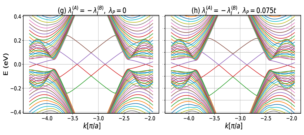
### Visual Description
# Technical Data Extraction: Electronic Band Structure Plots
This document provides a detailed technical extraction of the data and visual information contained in the provided image, which consists of two side-by-side electronic band structure plots, labeled (g) and (h).
## 1. General Metadata and Layout
* **Image Type:** Scientific line plots (Band structure diagrams).
* **Language:** English / Mathematical notation.
* **Layout:** Two panels arranged horizontally.
* **Left Panel:** Sub-figure (g).
* **Right Panel:** Sub-figure (h).
* **Common Y-Axis:** Energy $E$ measured in electronvolts (eV).
* **Common X-Axis:** Wavevector $k$ measured in units of $[\pi/a]$.
---
## 2. Axis and Scale Information
### Y-Axis (Energy)
* **Label:** $E \text{ (eV)}$
* **Range:** $-0.4$ to $0.4$
* **Major Tick Marks:** $-0.4, -0.2, 0.0, 0.2, 0.4$
* **Gridlines:** Horizontal grey lines at every major tick mark.
### X-Axis (Wavevector)
* **Label:** $k [\pi/a]$
* **Range:** Approximately $-4.4$ to $-1.8$
* **Major Tick Marks:** $-4.0, -3.5, -3.0, -2.5, -2.0$
* **Gridlines:** Vertical grey lines at every major tick mark.
---
## 3. Panel-Specific Data
### Panel (g)
* **Header Title:** $(g) \lambda_I^{(A)} = -\lambda_I^{(B)}, \lambda_P = 0$
* **Description:** This plot shows a band structure with a clear energy gap between the bulk bands, but with crossing "edge states" within the gap.
* **Key Features:**
* **Bulk Bands:** Multiple colored lines (blue, orange, green, red, purple, brown, pink, etc.) form dense manifolds above $E \approx 0.05$ eV and below $E \approx -0.05$ eV.
* **Gap States (Crossing):** Four distinct linear bands cross the Fermi level ($E = 0$).
* Two bands slope upward (positive group velocity) from $k \approx -3.8$ and $k \approx -2.2$.
* Two bands slope downward (negative group velocity) from $k \approx -3.8$ and $k \approx -2.2$.
* **Symmetry:** The plot is symmetric around $k = -3.0$. At $k = -3.0$, there is a crossing point at $E = 0$.
* **Topological Feature:** The crossing of bands at $E=0$ suggests a topological insulator phase or a similar state with protected edge modes.
### Panel (h)
* **Header Title:** $(h) \lambda_I^{(A)} = -\lambda_I^{(B)}, \lambda_P = 0.075t$
* **Description:** This plot shows the effect of introducing a non-zero $\lambda_P$ parameter.
* **Key Features:**
* **Bulk Bands:** The general structure of the bulk manifolds remains similar to panel (g), occupying the regions $|E| > 0.05$ eV.
* **Gap States (Modified):** The linear bands that crossed at $E=0$ in panel (g) are now modified.
* **Band Splitting:** There is a visible splitting or shifting in the energy levels of the edge states compared to panel (g). Specifically, the crossing points at $k \approx -3.8$ and $k \approx -2.2$ appear slightly more complex, with the "inner" crossing at $k = -3.0$ remaining, but the dispersion of the bands connecting the bulk to the crossing point is altered.
* **Local Extrema:** In the region $k \in [-4.0, -3.5]$ and $k \in [-2.5, -2.0]$, the bands within the gap show more pronounced "wiggles" or local maxima/minima compared to the smoother transitions in panel (g).
---
## 4. Component Isolation and Trend Analysis
### Bulk Manifolds (Header/Footer Regions)
* **Trend:** The bulk bands are parabolic-like near the gap edges ($k \approx -3.7$ and $k \approx -2.3$).
* **Density:** The bands are highly degenerate or closely spaced, indicated by the rainbow of colors (at least 15-20 distinct lines visible in both the valence and conduction regions).
### Gap Region (Main Chart Center)
* **Trend (g):** Linear crossings. The bands form an "X" shape centered at $k = -3.0, E = 0$.
* **Trend (h):** The "X" shape is preserved at the center, but the bands connecting to the bulk (around $E \approx \pm 0.2$) show increased curvature and energy shifts due to the $\lambda_P$ term.
## 5. Summary of Mathematical Parameters
* **$\lambda_I^{(A)} = -\lambda_I^{(B)}$**: Indicates staggered intrinsic spin-orbit coupling between sublattices A and B.
* **$\lambda_P$**: Represents a proximity-induced or potential-related term.
* In (g), $\lambda_P = 0$ (Symmetric case).
* In (h), $\lambda_P = 0.075t$ (Broken symmetry/Perturbed case).
</details>
Figure 6: Panels (a) and (b): Valley conductance vs. Rashba spin-orbit coupling $\lambda_{R}$ for $\Delta=0$ and $\Delta=0.02t$ , respectively. Panel (c) and (d) show the energy bands in the staggered case ( $\lambda_{I}^{(A)}=-\lambda_{I}^{(B)}$ ) for $\lambda_{R}=0.025t$ and $\lambda_{R}=0.075t$ , accordingly. Panels (e) and (f) show the conductance vs the strength of the PIA coupling. Panel (g) and (h) show the energy bands for $\lambda_{P}=0$ and $\lambda_{P}=0.075t$ , accordingly. Insets in (a, b, e, f) show spin-resolved valley conductance per valley.
In addition to the valley filtering, the interplay between the valley and spin degrees of freedom might realize new transport regimes. As shown in the inset of Fig. 6 (a) and (b), the wave functions around ${\bf K_{1}}$ or ${\bf K_{2}}$ (depending on the incident energy) are spin-dependent. Indeed, the Rashba coupling allows off-diagonal spin-flipping terms. Therefore, the spin conductance is also directly controlled by the Rashba strength, leading to valley-spin interplay dynamics. For a given incident energy, the spin-conductance $G_{\uparrow}({\bf K_{1}})$ oscillations have several phase shifts that correspond to the wavelengths of the oscillations determined by the Rashba coupling strength. Notice that the overall conductance of spin-polarized carriers, $G_{\uparrow}({\bf K_{1}})=G_{\uparrow\uparrow}({\bf K_{1}})+G_{\uparrow%
\downarrow}({\bf K_{1}})$ remains constant. Our calculations suggest valley processes dominate the conductance as spin-flips between neighboring sites require wider IQDs. Details on spin-dependent conductance in these proximity effect structures have been fully addressed in Ref. [29].
III.2.2 IQDs with lower- or higher-order symmetries
$C_{3v}$ symmetry is a property of hexagonal systems described by point group symmetry methods. To generalize the applicability of the model presented, it might be useful to lower (or raise) the symmetry of the IQDs. This strategy provides more options to describe novel regimes as it allows for removing (or adding) different spin-orbit terms. (i) In the case $\lambda_{R}=0$ , the point group is increased to $D_{3h}$ where the sublattice inversion asymmetry defines a point group of a planar system sustaining a triangular lattice with two staggered (non-equivalent) sublattices [27]. For such a case, the presence of the ISOC leads to the transmittance spectrum similar to Fig 2 (c) and (d). (ii) To lower the symmetry of the IQDs, one might include an additional staggered SOC term called PIA coupling (pseudospin inversion asymmetry for short). The spin-orbit Hamiltonian, in this case, will have an extra term:
$$
\displaystyle H_{PIA} \displaystyle= \displaystyle(\sqrt{3}a_{0}/2)\big{[}\lambda_{PIA}^{(A)}(\sigma_{z}+\sigma_{0}) \displaystyle+ \displaystyle\lambda_{PIA}^{(B)}(\sigma_{z}-\sigma_{0})\big{]}(k_{x}\sigma_{y}%
+k_{y}\sigma_{x}). \tag{7}
$$
where $\lambda_{PIA}^{(A)}$ and $\lambda_{PIA}^{(B)}$ are the staggered PIA coupling and $a_{0}$ is the lattice constant.
As shown in Fig. 6 (e) and (f), the PIA coupling does not affect the valley-conductance (even when it is a staggered spin-orbit term), neither for lower nor higher strength values. Therefore, we can confirm that only ISOC and RSOC control the valley process, as discussed in Fig. 2 and 6 (a, b). Hence, a QD with $\lambda_{PIA}≠ 0$ brings forth the same behavior as $\lambda_{PIA}=0$ , and a similar valley response will be observed. Indeed, the spectrum of the energy bands in Fig. 6 (g) and (h) supports these results, where we observe that for either neglected ( $\lambda_{PIA}=0$ ) or strong PIA terms ( $\lambda_{PIA}=0.075t$ ) the lower bulk and edge states are insensitive to the coupling strength.
This result is exciting as it implies that one might use TMDs to create IQDs with $C_{3v}$ -symmetry but with a $\lambda_{PIA}≠ 0$ without affecting their valley transport properties. Indeed, we might easily tune the intrinsic and Rashba parameters in such a system using TMD quantum dots. For instance, based on density functional theory fittings, both parameters are strongly sensitive to the electric field, twisting, and/or vertical strain effects [28, 46, 47]. The possibility of controlling the decrease or increase in the coupling strengths is highly desirable to monitor the valley polarization. Additionally, the spin-conductance is weakly affected (see inset of Fig. 6 (c, d)) by the presence of PIA as compared to Rashba terms. For more details about spin dependence and the effect of PIA coupling on spin polarization, see [48].
III.2.3 Valley confinement with IQDs
This subsection addresses the possibility of attaining confinement of valley-polarized electrons. Adopting the same sample parameters as in subsection III.1, we see that by zooming in on the transmission spectra from Fig. 2 (c, d), one can additionally recognize a resonance in the transmittance emerging in the IQDS, at $E_{F}=0.035t$ for higher values of ISOC ( $\lambda_{I}^{(A)}=-\lambda_{I}^{(B)}=0.065t$ ). The scattering through the induced region creates electron confinement for small-size IQDs ( $r_{0}=7$ nm). The resonance might be advantageously produced for weak ISOC at specific incident energy values. This case defines a real proximity effect where we tune $E_{F}$ to confine the valley states as shown in Sec. III.3.
<details>
<summary>x20.png Details</summary>
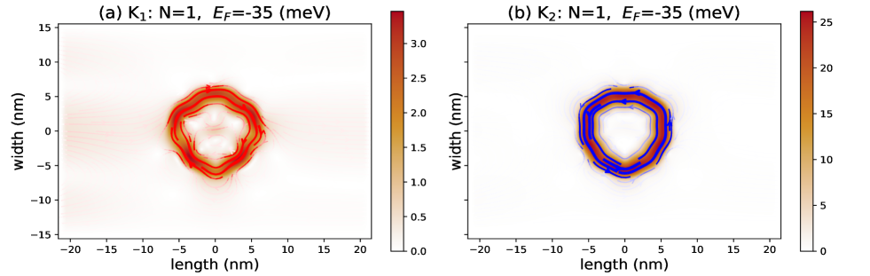
### Visual Description
# Technical Data Extraction: Spatial Current Distribution Plots
This document provides a comprehensive extraction of the data and visual information contained in the provided image, which consists of two side-by-side heatmaps representing physical simulations.
## 1. General Metadata
* **Image Type:** Scientific Heatmap / Contour Plot with Vector Overlays.
* **Language:** English.
* **Primary Units:** Nanometers (nm) for spatial dimensions; millielectronvolts (meV) for energy.
* **Common Axis Parameters:**
* **X-axis (Length):** Range from -20 to 20 nm. Markers at intervals of 5 units (-20, -15, -10, -5, 0, 5, 10, 15, 20).
* **Y-axis (Width):** Range from -15 to 15 nm. Markers at intervals of 5 units (-15, -10, -5, 0, 5, 10, 15).
---
## 2. Component Isolation: Panel (a)
### Header Information
* **Title:** (a) $K_1$: N=1, $E_F$=-35 (meV)
* **Interpretation:** This panel represents the $K_1$ valley/state for a single particle (N=1) at a Fermi energy of -35 meV.
### Main Chart Data
* **Spatial Distribution:** A central ring-like structure is located between -7 nm and +7 nm on the x-axis and -7 nm and +7 nm on the y-axis.
* **Visual Trend:** The intensity is concentrated in a hexagonal/circular ring. Inside the ring, there are three distinct "lobes" or sub-peaks of higher intensity arranged in a triangular pattern around the center (0,0).
* **Vector Overlay:** Red streamlines with arrows indicate the flow of current. The flow is **clockwise** around the central structure.
* **Intensity Scale (Colorbar):**
* **Location:** Right side of panel (a).
* **Range:** 0.0 to 3.0+ (top marker is 3.0, but the gradient extends slightly higher).
* **Color Gradient:** White (0.0) $\rightarrow$ Light Orange $\rightarrow$ Dark Red/Brown (~3.0).
---
## 3. Component Isolation: Panel (b)
### Header Information
* **Title:** (b) $K_2$: N=1, $E_F$=-35 (meV)
* **Interpretation:** This panel represents the $K_2$ valley/state for a single particle (N=1) at a Fermi energy of -35 meV.
### Main Chart Data
* **Spatial Distribution:** Similar to panel (a), a central ring-like structure is centered at (0,0), spanning roughly -7 nm to +7 nm in both dimensions.
* **Visual Trend:** The intensity distribution is more uniform along the ring compared to panel (a), forming a clearer hexagonal shape with a hollow center.
* **Vector Overlay:** Blue streamlines with arrows indicate the flow of current. The flow is **counter-clockwise** around the central structure.
* **Intensity Scale (Colorbar):**
* **Location:** Right side of panel (b).
* **Range:** 0 to 25.
* **Color Gradient:** White (0) $\rightarrow$ Orange $\rightarrow$ Dark Red (25).
* **Note:** The magnitude of the values in panel (b) is significantly higher (up to 25) compared to panel (a) (up to 3).
---
## 4. Comparative Analysis & Summary
| Feature | Panel (a) $K_1$ | Panel (b) $K_2$ |
| :--- | :--- | :--- |
| **Peak Magnitude** | ~3.0 - 3.5 | ~25.0 |
| **Current Direction** | Clockwise (Red arrows) | Counter-clockwise (Blue arrows) |
| **Internal Structure** | Three-lobed internal peaks | Uniform hexagonal ring |
| **Spatial Extent** | ~14 nm diameter | ~14 nm diameter |
**Technical Conclusion:**
The images depict the current density and flow for two different states ($K_1$ and $K_2$). While the spatial footprint of the current is similar in size and location for both, the $K_2$ state exhibits a current magnitude approximately 8 times stronger than the $K_1$ state. Crucially, the states exhibit opposite chirality (direction of flow), a characteristic often associated with valley-polarized transport in 2D materials like graphene or TMDs.
</details>
<details>
<summary>x21.png Details</summary>
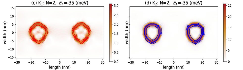
### Visual Description
# Technical Data Extraction: Spatial Distribution and Current Flow in Nanostructures
This document provides a detailed technical extraction of the data presented in the provided image, which consists of two side-by-side heatmaps with overlaid vector flow lines, likely representing physical properties (such as local density of states or current density) in a nanostructure.
## 1. Global Metadata and Parameters
The image contains two panels, labeled (c) and (d). Both panels share common physical parameters:
* **N (Number of units/particles):** 2
* **$E_F$ (Fermi Energy):** -35 (meV)
* **X-Axis (Length):** Measured in nanometers (nm), ranging from -30 to 30.
* **Y-Axis (Width):** Measured in nanometers (nm), ranging from -15 to 15.
---
## 2. Panel (c) Analysis: $K_1$ Distribution
### Header Information
* **Label:** (c) $K_1$: N=2, $E_F$=-35 (meV)
### Spatial Grounding and Components
* **Main Chart:** Displays two distinct circular/annular regions of intensity centered at approximately $x = -15$ nm and $x = +15$ nm along the $y = 0$ axis.
* **Color Scale (Right Side):** A vertical gradient bar ranging from **0.0 to 3.0**. The color transitions from white (0.0) to light orange, then to deep red/brown (3.0).
* **Flow Lines:** Overlaid on the intensity regions are bright red streamlines with arrowheads indicating direction.
### Data Trends and Observations
* **Intensity Distribution:** The intensity is concentrated in two ring-like structures. The peak intensity (darkest red, ~3.0 on the scale) forms a jagged, hexagonal-like perimeter around a lower-intensity center.
* **Current/Flow Direction:** The red streamlines indicate a **clockwise** circulation pattern around the center of each of the two structures.
* **Interaction:** There is very little "bleeding" or interaction between the two structures; the region at $x = 0$ shows near-zero intensity (white).
---
## 3. Panel (d) Analysis: $K_2$ Distribution
### Header Information
* **Label:** (d) $K_2$: N=2, $E_F$=-35 (meV)
### Spatial Grounding and Components
* **Main Chart:** Similar to panel (c), it displays two distinct annular regions centered at $x = -15$ nm and $x = +15$ nm.
* **Color Scale (Right Side):** A vertical gradient bar ranging from **0 to 25**. Note that the magnitude is significantly higher (nearly 8x) than in panel (c). The color transitions from white (0) to orange-brown (25).
* **Flow Lines:** Overlaid on the intensity regions are dark blue streamlines with arrowheads.
### Data Trends and Observations
* **Intensity Distribution:** The spatial footprint is nearly identical to panel (c), but the numerical values are much higher. The highest intensity (darkest brown, ~25) is concentrated in the outer ring of the structures.
* **Current/Flow Direction:** The blue streamlines indicate a **counter-clockwise** circulation pattern. This is the inverse of the flow direction observed in panel (c).
* **Symmetry:** The two structures (left and right) appear to be mirror images or identical copies of each other in terms of flow and intensity.
---
## 4. Comparative Summary Table
| Feature | Panel (c) - $K_1$ | Panel (d) - $K_2$ |
| :--- | :--- | :--- |
| **Max Scale Value** | 3.0 | 25 |
| **Flow Line Color** | Red | Blue |
| **Flow Direction** | Clockwise | Counter-clockwise |
| **Center Positions** | $x \approx \pm 15$ nm, $y \approx 0$ nm | $x \approx \pm 15$ nm, $y \approx 0$ nm |
| **Structure Shape** | Annular / Hexagonal Ring | Annular / Hexagonal Ring |
## 5. Conclusion
The data represents two distinct states or components ($K_1$ and $K_2$) of a system with two localized centers. While the spatial geometry of the intensity is consistent across both panels, $K_2$ exhibits a much higher magnitude and an opposite rotational flow compared to $K_1$. This likely represents valley-polarized or spin-polarized currents where $K_1$ and $K_2$ refer to different momentum space valleys.
</details>
Figure 7: Local density of valley-localized states near ${\bf K_{1}}$ (left) and ${\bf K_{2}}$ (right) at $E_{F}=0.035t$ , obtained for values of $\lambda_{I}^{(A)}=-\lambda_{I}^{(B)}=0.065t$ . The red and blue arrows show each valley state’s circulation direction. Panels (a, b) and (c, d) are for single and 2-chain-IQDs.
A detailed analysis of the local current profiles of valley states, as depicted in Fig. 7, shows a better representation of such a kind of valley-dependent electron confinement. Indeed, we observe that valley state confinement can be achieved by using either a single or a chain of IQDs. Importantly, the incident valley-states are trapped around the IQD region for appropriate SOC choices. This results in the confinement of the states, a process that can be regarded as the product of multiple internal reflections that trap the Dirac fermions by interference processes.
The system with symmetric IQDs appears to provide confinement for states at both valleys simultaneously in the same spatial region (we do not observe splittings of the valley confinement states). However, to achieve control over the valleys and multiple valleytronic and optoelectronic functionalities, using these IQDs, it will be necessary to create splittings and confining with unique quasi-bound states (belonging to either ${\bf K_{1}}$ or ${\bf K_{2}}$ ) in the local regions. The valley-bound states might be split by considering asymmetric quantum dots with different shapes and point group symmetries. This topic will be addressed in future work.
III.3 Realistic IQDs in heterostructures of twisted graphene and TMD monolayers
As discussed in Sec. III.2.2 and III.2.3, a quantitative study of the model has been addressed in the case of weak SOCs. To provide a comprehensive picture of concrete setups, we perform a real case study and show how an IQD might be realized in realistic experimental conditions.
To start, we consider IQDs produced with four different semiconducting TMDs islands: MoSe 2, WSe 2, MoS 2, and WS 2 deposited on graphene monolayer, as shown in Fig. 1 (b). Furthermore, we analyze the proximity-induced spin-orbit couplings in the case of twisted TMDs on graphene. Based on the work of T. Naimer et et al. [35], twisting leads to tuning the magnitudes of the valley-Zeeman and Rashba spin-orbit couplings. Interestingly, the amplitude of the staggered potential $\Delta$ in twisted G-TMDs is significantly weak and tends to zero at some specific twisting angles, thus favoring valley filtering, as discussed in Fig. 4. Based on the tight-binding parameters derived from first principles calculations [35], we compute the valley conductance through four $(n=4)$ IQDs at $E_{F}=0.035t\simeq 0.095$ meV and show results in Fig. 8.
<details>
<summary>x22.png Details</summary>
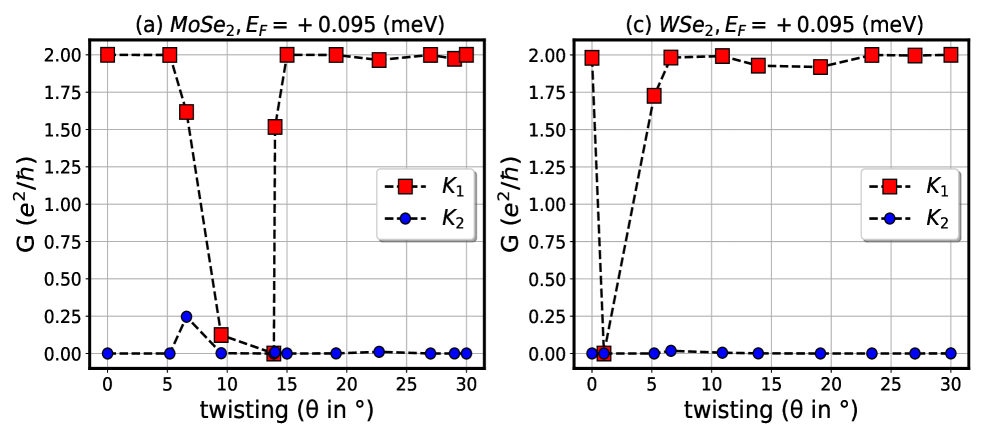
### Visual Description
# Technical Data Extraction: Conductance vs. Twisting Angle in $MoSe_2$ and $WSe_2$
This document provides a comprehensive extraction of data from two side-by-side line charts illustrating the relationship between twisting angle ($\theta$) and conductance ($G$) for two different materials.
## 1. General Metadata
* **Language:** English
* **Image Type:** Scientific Data Plots (Line charts with markers)
* **Common Y-Axis:** Conductance $G$ in units of $(e^2/h)$
* **Common X-Axis:** twisting ($\theta$ in $^\circ$)
* **Common Legend:**
* **Red Squares with dashed black line:** $K_1$
* **Blue Circles with dashed black line:** $K_2$
* **Legend Location:** Center-right of each plot.
---
## 2. Plot (a): $MoSe_2, E_F = +0.095$ (meV)
### Component Isolation: Header & Axes
* **Title:** (a) $MoSe_2, E_F = +0.095$ (meV)
* **Y-Axis Range:** 0.00 to 2.00 (increments of 0.25)
* **X-Axis Range:** 0 to 30 (increments of 5)
### Data Series Analysis
#### Series $K_1$ (Red Squares)
* **Trend:** Starts at a maximum value of 2.00. Remains stable until $\sim 5^\circ$, then drops sharply toward zero at $\sim 14^\circ$. It then recovers instantly back to 2.00 and remains stable through $30^\circ$.
* **Key Data Points (Approximate):**
| $\theta$ ($^\circ$) | $G$ ($e^2/h$) |
| :--- | :--- |
| 0 | 2.00 |
| 5 | 2.00 |
| 6.5 | 1.60 |
| 9.5 | 0.15 |
| 13.8 | 0.00 |
| 14 | 1.50 |
| 15 | 2.00 |
| 19 | 2.00 |
| 22.5 | 1.95 |
| 27 | 2.00 |
| 29 | 1.95 |
| 30 | 2.00 |
#### Series $K_2$ (Blue Circles)
* **Trend:** Remains consistently at or near 0.00 for the entire range, with a single small peak occurring between $5^\circ$ and $10^\circ$.
* **Key Data Points (Approximate):**
| $\theta$ ($^\circ$) | $G$ ($e^2/h$) |
| :--- | :--- |
| 0 | 0.00 |
| 5 | 0.00 |
| 6.5 | 0.25 |
| 9.5 | 0.00 |
| 14 | 0.00 |
| 30 | 0.00 |
---
## 3. Plot (c): $WSe_2, E_F = +0.095$ (meV)
### Component Isolation: Header & Axes
* **Title:** (c) $WSe_2, E_F = +0.095$ (meV)
* **Y-Axis Range:** 0.00 to 2.00 (increments of 0.25)
* **X-Axis Range:** 0 to 30 (increments of 5)
### Data Series Analysis
#### Series $K_1$ (Red Squares)
* **Trend:** Starts at 2.00, immediately drops to 0.00 at a very low angle ($\sim 1^\circ$), then recovers steadily back to 2.00 by $\sim 11^\circ$, remaining mostly stable at the maximum thereafter.
* **Key Data Points (Approximate):**
| $\theta$ ($^\circ$) | $G$ ($e^2/h$) |
| :--- | :--- |
| 0 | 2.00 |
| 1 | 0.00 |
| 5 | 1.75 |
| 6.5 | 1.98 |
| 11 | 2.00 |
| 14 | 1.95 |
| 19 | 1.95 |
| 23.5 | 2.00 |
| 27 | 2.00 |
| 30 | 2.00 |
#### Series $K_2$ (Blue Circles)
* **Trend:** Extremely stable. The value remains at 0.00 for the entire duration of the twisting angle from $0^\circ$ to $30^\circ$.
* **Key Data Points (Approximate):**
| $\theta$ ($^\circ$) | $G$ ($e^2/h$) |
| :--- | :--- |
| 0 | 0.00 |
| 1 | 0.00 |
| 30 | 0.00 |
---
## 4. Comparative Summary
* **Material Difference:** In $MoSe_2$, the $K_1$ conductance dip occurs at a much higher twisting angle ($\sim 14^\circ$) compared to $WSe_2$, where the dip occurs almost immediately ($\sim 1^\circ$).
* **$K_2$ Activity:** $MoSe_2$ shows a slight resonance/increase in $K_2$ conductance around $6.5^\circ$, whereas $WSe_2$ shows no $K_2$ activity across the measured spectrum.
* **Quantization:** Both materials exhibit quantized conductance behavior, primarily switching between $G=0$ and $G=2$ $(e^2/h)$ for the $K_1$ channel.
</details>
<details>
<summary>x23.png Details</summary>
### Visual Description
# Technical Data Extraction: Conductance vs. Twisting Angle in $MoSe_2$ and $WSe_2$
This document provides a comprehensive extraction of data from two side-by-side line charts illustrating the relationship between twisting angle ($\theta$) and conductance ($G$) for two different materials.
## 1. General Metadata
* **Language:** English
* **Image Type:** Scientific Data Plots (Line charts with markers)
* **Common Y-Axis:** $G$ ($e^2/h$) - Conductance in units of the conductance quantum.
* **Common X-Axis:** twisting ($\theta$ in $^\circ$) - Twisting angle in degrees.
* **Common Legend:**
* **Blue Circles ($K_1$):** Represent data series for $K_1$.
* **Red Squares ($K_2$):** Represent data series for $K_2$.
* **Line Style:** Dashed black lines connecting markers.
* **Fermi Energy ($E_F$):** Constant at $-0.095$ (meV) for both plots.
---
## 2. Plot (b): $MoSe_2, E_F = -0.095$ (meV)
### Component Isolation: Header & Axes
* **Title:** (b) $MoSe_2, E_F = -0.095$ (meV)
* **Y-Axis Range:** $0.00$ to $2.00$ (increments of $0.25$)
* **X-Axis Range:** $0$ to $30$ (increments of $5$)
* **Legend Location:** Right-center $[x \approx 0.8, y \approx 0.5]$
### Trend Analysis
* **Series $K_1$ (Blue Circles):** Starts at a maximum value of $2.0$. It remains stable until $\theta \approx 5^\circ$, then drops sharply to near $0$ at $\theta \approx 10^\circ-14^\circ$. It then exhibits a vertical-like recovery back to $2.0$ at $\theta \approx 15^\circ$ and remains stable at $2.0$ through $30^\circ$.
* **Series $K_2$ (Red Squares):** Remains consistently at $0.0$ for almost the entire range, with a single small peak (upward slope then downward) occurring between $\theta \approx 5^\circ$ and $10^\circ$.
### Data Point Extraction (Approximate)
| Twisting $\theta$ ($^\circ$) | $K_1$ Conductance ($e^2/h$) | $K_2$ Conductance ($e^2/h$) |
| :--- | :--- | :--- |
| 0 | 2.00 | 0.00 |
| 5 | 2.00 | 0.00 |
| 6.5 | 1.60 | 0.25 |
| 9.5 | 0.12 | 0.00 |
| 13.5 | 0.00 | 0.00 |
| 14 | 1.50 | 0.00 |
| 15 | 2.00 | 0.00 |
| 19 | 2.00 | 0.00 |
| 23 | 1.95 | 0.01 |
| 27 | 2.00 | 0.00 |
| 29 | 1.98 | 0.00 |
| 30 | 2.00 | 0.00 |
---
## 3. Plot (d): $WSe_2, E_F = -0.095$ (meV)
### Component Isolation: Header & Axes
* **Title:** (d) $WSe_2, E_F = -0.095$ (meV)
* **Y-Axis Range:** $0.00$ to $2.00$ (increments of $0.25$)
* **X-Axis Range:** $0$ to $30$ (increments of $5$)
* **Legend Location:** Right-center $[x \approx 0.8, y \approx 0.5]$
### Trend Analysis
* **Series $K_1$ (Blue Circles):** Starts at $2.0$. It experiences an extremely sharp drop to $0.0$ at a very low angle ($\theta \approx 1^\circ$). It then slopes upward rapidly, returning to $2.0$ by $\theta \approx 10^\circ$ and maintaining that value (with minor fluctuations) until $30^\circ$.
* **Series $K_2$ (Red Squares):** Shows a flat trend line. The conductance remains at $0.0$ across the entire twisting angle range from $0^\circ$ to $30^\circ$.
### Data Point Extraction (Approximate)
| Twisting $\theta$ ($^\circ$) | $K_1$ Conductance ($e^2/h$) | $K_2$ Conductance ($e^2/h$) |
| :--- | :--- | :--- |
| 0 | 2.00 | 0.00 |
| 1 | 0.00 | 0.00 |
| 5 | 1.72 | 0.00 |
| 6.5 | 1.98 | 0.01 |
| 11 | 2.00 | 0.00 |
| 14 | 1.92 | 0.00 |
| 19 | 1.92 | 0.00 |
| 23 | 2.00 | 0.00 |
| 27 | 2.00 | 0.00 |
| 30 | 2.00 | 0.00 |
---
## 4. Summary of Observations
* **Material Comparison:** $MoSe_2$ shows a "conductance gap" or dip in the $K_1$ channel at a much higher twisting angle ($\approx 10^\circ-14^\circ$) compared to $WSe_2$, where the dip occurs almost immediately ($\approx 1^\circ$).
* **Channel Dominance:** In both materials, the $K_1$ channel (blue) is the primary carrier of conductance, maintaining a value of $2.0$ for most angles, while the $K_2$ channel (red) remains largely suppressed at $0.0$.
</details>
<details>
<summary>x24.png Details</summary>
### Visual Description
# Technical Data Extraction: MoSe2 Current Density and Flow Maps
This document provides a detailed technical extraction of the data contained in the provided image, which consists of two side-by-side scientific plots (labeled 'e' and 'f') representing physical simulations of MoSe2.
## 1. General Metadata
* **Material:** MoSe2 (Molybdenum diselenide)
* **Fermi Energy ($E_F$):** 95 (meV)
* **Angle ($\theta$):** 15°
* **Language:** English
---
## 2. Component Isolation: Plot (e)
### Header Information
* **Label:** (e)
* **Title:** MoSe2: $E_F=95$ (meV), $\theta=15°$
### Axis and Scale
* **X-axis (Horizontal):** labeled "length (nm)". Range: -40 to 40. Major ticks at -40, -20, 0, 20, 40.
* **Y-axis (Vertical):** labeled "width (nm)". Range: -15 to 15. Major ticks at -10, 0, 10.
* **Color Bar (Right):** Vertical scale representing a magnitude (likely current density). Range: 0.0 to >0.3. Ticks at 0.0, 0.1, 0.2, 0.3. Color gradient: Light cream (0.0) to Dark Red (~0.4).
### Data Visualization & Trends
* **Type:** Streamline plot overlaid on a heatmap.
* **Heatmap Trend:** The intensity is highest (dark red) along the top and bottom edges of the channel (approx. $y = \pm 10$ nm) and at the left entrance ($x = -40$ nm). There are two distinct circular "voids" or low-intensity regions (white) centered at approximately $x = -15, y = 0$ and $x = 15, y = 0$.
* **Streamline Flow:**
* Flow enters from the left ($x = -40$).
* The streamlines exhibit turbulent or vortex-like behavior near the left boundary.
* As the flow moves right, it splits to go around the two central low-intensity circular regions.
* The flow is most laminar and concentrated (indicated by darker red streamlines) in the regions between the central voids and the outer boundaries ($y \approx \pm 10$).
---
## 3. Component Isolation: Plot (f)
### Header Information
* **Label:** (f)
* **Title:** MoSe2: $E_F=95$ (meV), $\theta=15°$
### Axis and Scale
* **X-axis (Horizontal):** labeled "length (nm)". Range: -40 to 40. Major ticks at -40, -20, 0, 20, 40.
* **Y-axis (Vertical):** labeled "width (nm)". Range: -15 to 15. Major ticks at -10, 0, 10.
* **Color Bar (Right):** Vertical scale. Range: 0.0 to >0.4. Ticks at 0.0, 0.1, 0.2, 0.3, 0.4. Color gradient: Light cream (0.0) to Dark Red (~0.45).
### Data Visualization & Trends
* **Type:** Vector/Streamline plot with localized heatmap.
* **Heatmap Trend:** Unlike plot (e), the data in plot (f) is heavily concentrated at the left boundary ($x = -40$ to $x \approx -20$). The rest of the plot ($x > -20$) is white, indicating zero or negligible values.
* **Streamline Flow:**
* The flow consists of two primary counter-rotating vortices located at the left edge.
* **Upper Vortex:** Centered around $y \approx 5$, rotating counter-clockwise.
* **Lower Vortex:** Centered around $y \approx -5$, rotating clockwise.
* The streamlines are colored blue, contrasting with the red/orange heatmap background at the very edge ($x = -40$).
* The flow appears to be "injected" at $y=0, x=-40$ and then curls back toward the corners at $x=-40, y=\pm 12$.
---
## 4. Comparative Summary
| Feature | Plot (e) | Plot (f) |
| :--- | :--- | :--- |
| **Spatial Coverage** | Full channel (-40 to 40 nm) | Left-loaded (-40 to -20 nm) |
| **Flow Pattern** | Channel flow bypassing two central obstacles | Two localized vortices at the injection point |
| **Max Intensity** | ~0.35 (distributed) | >0.4 (highly localized at $x=-40$) |
| **Symmetry** | Roughly symmetric across $y=0$ | Highly symmetric across $y=0$ |
**Note on Spatial Grounding:** The color bars for both plots are located at the far right of each respective sub-figure. In plot (e), the dark red streamlines at $y=10$ match the $\approx 0.3$ value on the legend. In plot (f), the dark orange/red patch at $x=-40, y=0$ matches the $\approx 0.4$ value on its respective legend.
</details>
<details>
<summary>x25.png Details</summary>
### Visual Description
# Technical Data Extraction: MoSe2 Current Density and Streamline Analysis
This document provides a detailed technical extraction of the data presented in the provided image, which consists of two side-by-side heatmaps with overlaid streamlines, labeled (g) and (h).
## 1. General Metadata
* **Subject Matter:** Physics/Materials Science simulation of Molybdenum Diselenide (MoSe2).
* **Parameters (Common to both):**
* **Fermi Energy ($E_F$):** -95 (meV)
* **Twist Angle ($\theta$):** 15°
* **Coordinate System:**
* **X-axis:** length (nm), ranging from -40 to 40.
* **Y-axis:** width (nm), ranging from approximately -15 to 15 (ticks at -10, 0, 10).
---
## 2. Component Analysis: Plot (g)
### Header Information
* **Label:** (g)
* **Title:** MoSe2: $E_F$=-95 (meV), $\theta$=15°
### Spatial Data & Trends
* **Region Isolation:** The data is heavily concentrated on the left side of the plot (length -40 nm to -20 nm). The rest of the plot (length -20 nm to 40 nm) is white/null, indicating zero or negligible magnitude.
* **Heatmap (Magnitude):**
* **Color Scale:** Located at the right of the plot. A gradient from white (0.0) to dark red (~0.45).
* **Peak Intensity:** Reaches values > 0.4 near the left boundary (length = -40 nm) at widths of approximately ±10 nm.
* **Streamlines (Flow):**
* **Visual Trend:** Red streamlines originate from the left boundary. They curve inward toward the center (width = 0) and then dissipate as they move toward length = -20 nm.
* **Directionality:** The arrows indicate flow moving from the left edge toward the center-right of the localized active zone.
---
## 3. Component Analysis: Plot (h)
### Header Information
* **Label:** (h)
* **Title:** MoSe2: $E_F$=-95 (meV), $\theta$=15°
### Spatial Data & Trends
* **Region Isolation:** Unlike plot (g), data is distributed across the entire length (-40 nm to 40 nm).
* **Heatmap (Magnitude):**
* **Color Scale:** Located at the right of the plot. A gradient from white (0.0) to dark red (~0.35). Note the maximum scale is lower than in plot (g).
* **Pattern:** Shows a periodic or "wavy" distribution of intensity. Higher magnitudes (light orange/brown) are seen in horizontal bands near width ±10 nm.
* **Streamlines (Flow):**
* **Visual Trend:** Blue streamlines dominate this plot. They exhibit a complex, oscillatory flow pattern across the entire length.
* **Vortices/Features:** There are two distinct "eye" or depletion regions (white areas) centered at approximately:
1. Length ≈ -15 nm, Width ≈ 0 nm
2. Length ≈ 15 nm, Width ≈ 0 nm
* **Flow Path:** The streamlines flow around these central white regions, creating a wave-like motion that propagates from left to right across the channel.
---
## 4. Comparative Data Summary
| Feature | Plot (g) | Plot (h) |
| :--- | :--- | :--- |
| **Max Magnitude Scale** | ~0.45 | ~0.35 |
| **Spatial Distribution** | Localized (Left side) | Distributed (Full length) |
| **Streamline Color** | Red | Blue |
| **Flow Characteristic** | Convergent/Dissipative | Periodic/Oscillatory |
| **Key Feature** | High intensity at injection point | Periodic "voids" at ±15nm length |
---
## 5. Axis and Legend Details
### X-Axis (Length)
* **Label:** length (nm)
* **Markers:** -40, -20, 0, 20, 40
### Y-Axis (Width)
* **Label:** width (nm)
* **Markers:** -10, 0, 10
### Colorbar (Z-Axis / Magnitude)
* **Plot (g) Ticks:** 0.0, 0.1, 0.2, 0.3, 0.4
* **Plot (h) Ticks:** 0.0, 0.1, 0.2, 0.3
</details>
Figure 8: Panels (a) and (b) show valley conductance vs twist angle $\theta$ for IQDs made of MoSe 2 on graphene at $E_{F}=0.095$ meV and $-0.095$ meV, respectively. Panels (c) and (d) correspond to IQDs of WSe 2 on graphene for the same values of $E_{F}$ . In panels (e)-(f) and (g)-(h) we show valley-polarized currents for MoSe 2 for positive and negative bias ( $E_{F}$ ), respectively
.
Valley transmittance with first propagating modes in twisted TMDs: It is important to state that in all previous sections, we considered the transmittance spectrum at $E_{F}=± 0.035t$ ; a value that ensures that the valley-dependent conductance is addressed independently with the simultaneous excitation of the first propagating modes in ${\bf K_{1}}$ and ${\bf K_{2}}$ since the Fermi energy $E_{F}$ is larger than the valley-mode spacing gap. For more details, refer to our previous work [49].
In Fig. 8, we inject electrons with $E_{F}=± 0.095$ meV into four identical IQDs produced with MoSe 2 and WSe 2 islands. The induced SOCs are tuned by twisting the TMDs and allow for monitoring of the valley response in the system. At positive incident energy, the valley conductance from valley ${\bf K_{1}},({\bf K_{2}})$ is 2 (0) in the units of $e^{2}/\hbar$ . Only electrons from either valley ${\bf K_{1}}$ or ${\bf K_{2}}$ go through the system (see panels (a) and (c)). As previously discussed, we also confirm that changing the Fermi energy sign reverses the valley polarity, as shown in Fig. 8 (b) and (d). Additionally, as shown in 8 (a) and (b), twisting in the case of MoSe 2 (that induces a weak staggered potential [35]) leads to control of valley transmittances similar to what we found when discussing the model with weak couplings in Fig. 6.
The obtained results with MoSe 2 can be applied to obtain pure valley polarized conductances with the twist angle outside the limits of $9^{\circ}-14^{\circ}$ . Hence, the valley transmission from ${\bf K_{1}}$ ( ${\bf K_{2}}$ ) jumps almost from 2 to 0 for positive (negative) incident energy, depending on twisting angles and full valley polarized currents. To emphasize these findings, we plot the local current for $\theta=15^{\circ}$ at $E_{F}=0.095$ meV ( $-0.095$ meV) for MoSe 2 (WSe 2). Indeed, one observes that only one valley is scattered, which leads to conducting Hall currents depending on the sign of the incident Fermi-energy. These results are important compared to those shown in Fig. 5, where both valleys conduct through bulk and Hall currents. Hence, the IQDs based on semiconducting TMDs MoSe 2 and WSe 2 might be used as promising islands for generating valley Hall signals.
<details>
<summary>x26.png Details</summary>
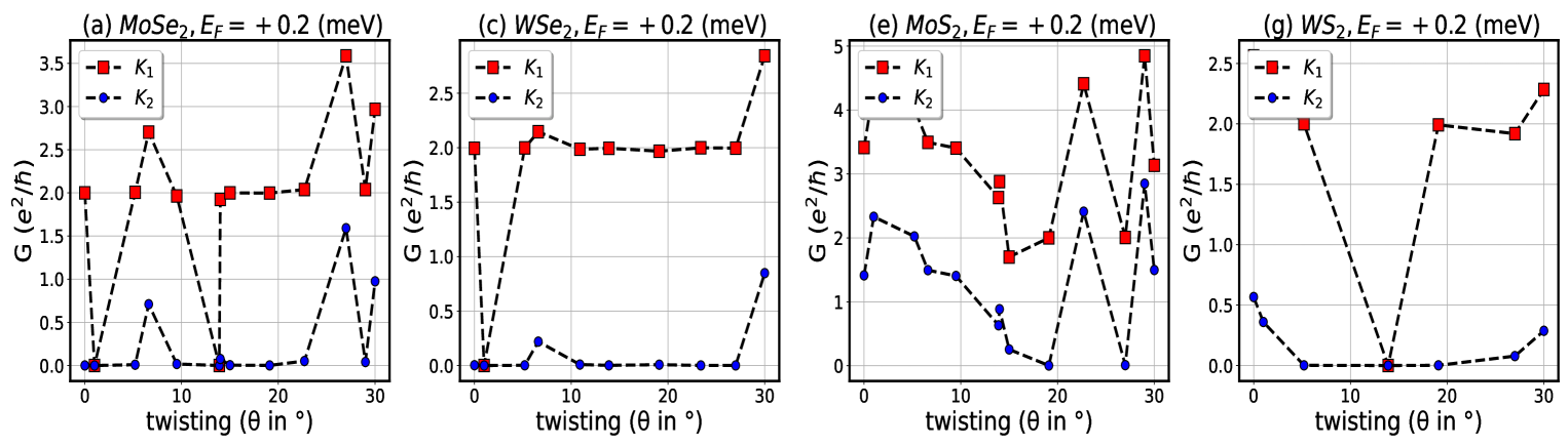
### Visual Description
# Technical Data Extraction: Conductance vs. Twisting Angle in Transition Metal Dichalcogenides
This document provides a comprehensive extraction of data from a series of four scientific plots showing the relationship between conductance ($G$) and twisting angle ($\theta$) for different materials at a specific Fermi energy ($E_F = +0.2$ meV).
## 1. General Metadata and Global Parameters
* **Image Type:** Multi-panel line graph (4 panels).
* **Common X-axis:** twisting ($\theta$ in $^\circ$). Range: 0 to 30.
* **Common Y-axis:** $G$ ($e^2/h$). Range varies by panel.
* **Common Legend:**
* **Red Squares (dashed line):** $K_1$ (Valley 1)
* **Blue Circles (dashed line):** $K_2$ (Valley 2)
* **Fermi Energy ($E_F$):** Constant at $+0.2$ meV for all panels.
* **Language:** English.
---
## 2. Panel Analysis
### Panel (a): $MoSe_2$
* **Header:** (a) $MoSe_2, E_F = +0.2$ (meV)
* **Y-axis Range:** 0.0 to 3.5+
* **Trend Analysis:**
* **$K_1$ (Red):** Starts at 2.0, fluctuates significantly with sharp peaks at $\sim 7^\circ$ and $\sim 27^\circ$. It drops to near zero at $\sim 14^\circ$.
* **$K_2$ (Blue):** Remains very low (near 0) for most angles, with small peaks at $\sim 7^\circ$ and a significant spike to $\sim 1.6$ at $\sim 27^\circ$.
* **Approximate Data Points:**
* $\theta \approx 0$: $K_1 \approx 2.0, K_2 \approx 0.0$
* $\theta \approx 7$: $K_1 \approx 2.7, K_2 \approx 0.7$
* $\theta \approx 14$: $K_1 \approx 0.0, K_2 \approx 0.0$
* $\theta \approx 27$: $K_1 \approx 3.6, K_2 \approx 1.6$
* $\theta \approx 30$: $K_1 \approx 3.0, K_2 \approx 1.0$
### Panel (c): $WSe_2$
* **Header:** (c) $WSe_2, E_F = +0.2$ (meV)
* **Y-axis Range:** 0.0 to 2.5+
* **Trend Analysis:**
* **$K_1$ (Red):** Shows a "plateau" behavior. After an initial drop at $1^\circ$, it stays remarkably stable near $G=2.0$ from $5^\circ$ to $27^\circ$, before spiking at $30^\circ$.
* **$K_2$ (Blue):** Almost entirely suppressed (near 0) across the whole range, except for a small rise at $30^\circ$.
* **Approximate Data Points:**
* $\theta \approx 0$: $K_1 \approx 2.0, K_2 \approx 0.0$
* $\theta \approx 1$: $K_1 \approx 0.0, K_2 \approx 0.0$
* $\theta \approx 10-25$: $K_1 \approx 2.0, K_2 \approx 0.0$
* $\theta \approx 30$: $K_1 \approx 2.8, K_2 \approx 0.8$
### Panel (e): $MoS_2$
* **Header:** (e) $MoS_2, E_F = +0.2$ (meV)
* **Y-axis Range:** 0 to 5
* **Trend Analysis:**
* **$K_1$ (Red):** Highly oscillatory. High values ($>3$) at low angles, a dip near $15^\circ$, a massive peak at $\sim 23^\circ$, another dip, and a final peak at $29^\circ$.
* **$K_2$ (Blue):** Follows a similar oscillatory pattern to $K_1$ but at a lower magnitude (generally between 0 and 2.5).
* **Approximate Data Points:**
* $\theta \approx 0$: $K_1 \approx 3.4, K_2 \approx 1.4$
* $\theta \approx 15$: $K_1 \approx 1.7, K_2 \approx 0.3$
* $\theta \approx 23$: $K_1 \approx 4.4, K_2 \approx 2.4$
* $\theta \approx 29$: $K_1 \approx 4.8, K_2 \approx 2.8$
### Panel (g): $WS_2$
* **Header:** (g) $WS_2, E_F = +0.2$ (meV)
* **Y-axis Range:** 0.0 to 2.5
* **Trend Analysis:**
* **$K_1$ (Red):** Data is missing for low angles ($<5^\circ$). It starts high at $\sim 2.0$, drops to zero at the midpoint ($\sim 14^\circ$), then recovers to $\sim 2.0$ and stays relatively flat until a final rise at $30^\circ$.
* **$K_2$ (Blue):** Starts at $\sim 0.6$, decays to zero by $5^\circ$, stays at zero until $\sim 25^\circ$, then rises slightly.
* **Approximate Data Points:**
* $\theta \approx 0$: $K_1 = \text{N/A}, K_2 \approx 0.6$
* $\theta \approx 5$: $K_1 \approx 2.0, K_2 \approx 0.0$
* $\theta \approx 14$: $K_1 \approx 0.0, K_2 \approx 0.0$
* $\theta \approx 20$: $K_1 \approx 2.0, K_2 \approx 0.0$
* $\theta \approx 30$: $K_1 \approx 2.3, K_2 \approx 0.3$
---
## 3. Component Isolation Summary
| Region | Content Description |
| :--- | :--- |
| **Header** | Contains panel labels (a, c, e, g) and material/energy specs. |
| **Main Chart Area** | Four sub-plots with dashed lines connecting data points. Grid lines are present. |
| **Legend** | Located in the top-left of each sub-plot. Red Square = $K_1$, Blue Circle = $K_2$. |
| **Footer** | Contains the X-axis label "twisting ($\theta$ in $^\circ$)" repeated for each column. |
## 4. Key Observations
1. **Symmetry/Dips:** Most materials show a significant drop in conductance ($G \rightarrow 0$) near the middle of the angular range (around $14^\circ - 15^\circ$).
2. **Valley Dominance:** In almost all cases, the $K_1$ valley (red) contributes significantly more to the total conductance than the $K_2$ valley (blue).
3. **Material Variation:** $MoS_2$ exhibits the highest absolute conductance values (peaking near 5 $e^2/h$), while $WSe_2$ shows the most stable conductance plateau.
</details>
<details>
<summary>x27.png Details</summary>
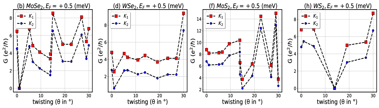
### Visual Description
# Technical Data Extraction: Conductance vs. Twisting Angle in Transition Metal Dichalcogenides
This document provides a comprehensive extraction of data from a series of four scientific plots showing the relationship between conductance ($G$) and twisting angle ($\theta$) for different materials at a fixed Fermi energy ($E_F = +0.5$ meV).
## 1. General Metadata
* **Image Type:** Multi-panel line graph (4 panels).
* **Y-Axis Label (All Panels):** $G$ ($e^2/h$) - Conductance in units of the conductance quantum.
* **X-Axis Label (All Panels):** twisting ($\theta$ in $^\circ$) - Twisting angle in degrees.
* **X-Axis Range:** $0^\circ$ to $30^\circ$.
* **Legend (All Panels):**
* **Red Squares (dashed line):** $K_1$
* **Blue Circles (dashed line):** $K_2$
* **Legend Location:** Top-left of each plot area.
* **Common Features:** All plots show a highly oscillatory behavior with $K_1$ consistently maintaining higher conductance values than $K_2$ across most angles.
---
## 2. Panel (b): $MoSe_2, E_F = +0.5$ (meV)
### Trend Analysis
* **$K_1$ (Red):** Starts high (~6.5), drops sharply to 0 at $\theta \approx 1^\circ$, then exhibits a "W" shaped oscillation between $5^\circ$ and $15^\circ$, peaking near 8.5 at $15^\circ$. It stabilizes around 5.0 between $20^\circ-25^\circ$ before a final peak at $28^\circ$.
* **$K_2$ (Blue):** Follows a similar oscillatory pattern but at a lower magnitude. It also hits 0 at $\theta \approx 1^\circ$.
### Data Points (Approximate)
| Twisting $\theta$ ($^\circ$) | $K_1$ Conductance ($e^2/h$) | $K_2$ Conductance ($e^2/h$) |
| :--- | :--- | :--- |
| 0 | 6.5 | 4.5 |
| 1 | 0.0 | 0.0 |
| 5 | 6.8 | 4.8 |
| 7 | 4.9 | 3.0 |
| 14 | 3.3 | 1.5 |
| 15 | 8.5 | 6.5 |
| 19 | 5.0 | 3.1 |
| 23 | 5.0 | 3.1 |
| 27 | 8.1 | 6.1 |
| 29 | 5.4 | 3.4 |
| 30 | 6.8 | 4.9 |
---
## 3. Panel (d): $WSe_2, E_F = +0.5$ (meV)
### Trend Analysis
* **$K_1$ (Red):** Relatively stable compared to other panels. It fluctuates between 4.0 and 5.0 for most of the range before a sharp spike to ~9.5 at $30^\circ$.
* **$K_2$ (Blue):** Shows a significant dip to near 0 at $\theta \approx 1^\circ$, then remains consistently lower than $K_1$ (between 2.0 and 3.0) until a sharp rise to ~7.5 at $30^\circ$.
### Data Points (Approximate)
| Twisting $\theta$ ($^\circ$) | $K_1$ Conductance ($e^2/h$) | $K_2$ Conductance ($e^2/h$) |
| :--- | :--- | :--- |
| 0 | 4.8 | 2.8 |
| 1 | 2.6 | 0.6 |
| 5 | 4.7 | 2.7 |
| 7 | 4.3 | 2.7 |
| 11 | 4.0 | 2.3 |
| 14 | 4.5 | 2.5 |
| 19 | 3.7 | 1.8 |
| 23 | 4.1 | 2.2 |
| 27 | 4.2 | 2.2 |
| 30 | 9.5 | 7.4 |
---
## 4. Panel (f): $MoS_2, E_F = +0.5$ (meV)
### Trend Analysis
* **$K_1$ (Red):** Shows a gradual upward trend from $0^\circ$ to $14^\circ$, followed by a sharp drop to ~4.0 at $15^\circ$. It then recovers with a massive peak of ~14.5 at $23^\circ$ and another peak at $29^\circ$.
* **$K_2$ (Blue):** Mirrors the $K_1$ trend closely but shifted down by approximately 2 units. It reaches its lowest point (~2.2) at $15^\circ$.
### Data Points (Approximate)
| Twisting $\theta$ ($^\circ$) | $K_1$ Conductance ($e^2/h$) | $K_2$ Conductance ($e^2/h$) |
| :--- | :--- | :--- |
| 0 | 8.8 | 6.8 |
| 1 | 8.2 | 6.2 |
| 5 | 8.3 | 6.3 |
| 7 | 8.4 | 6.4 |
| 10 | 9.8 | 7.8 |
| 14 | 10.4 | 8.4 |
| 15 | 3.8 | 2.2 |
| 19 | 6.4 | 4.3 |
| 23 | 14.5 | 12.5 |
| 27 | 6.1 | 4.2 |
| 29 | 15.0 | 13.0 |
| 30 | 3.8 | 2.7 |
---
## 5. Panel (h): $WS_2, E_F = +0.5$ (meV)
### Trend Analysis
* **$K_1$ (Red):** Starts at ~6.8, maintains this until $5^\circ$, then drops linearly to 0 at $\theta \approx 14^\circ$. It then recovers steadily, ending at a peak of ~8.8 at $30^\circ$.
* **$K_2$ (Blue):** Follows the same "V" shape as $K_1$. It starts lower (~4.8), hits 0 at $14^\circ$, and ends at ~6.8 at $30^\circ$.
### Data Points (Approximate)
| Twisting $\theta$ ($^\circ$) | $K_1$ Conductance ($e^2/h$) | $K_2$ Conductance ($e^2/h$) |
| :--- | :--- | :--- |
| 0 | 6.8 | 4.8 |
| 1 | 6.8 | 5.4 |
| 5 | 6.8 | 4.9 |
| 14 | 0.0 | 0.0 |
| 19 | 5.0 | 3.0 |
| 27 | 5.4 | 3.5 |
| 30 | 8.8 | 6.8 |
</details>
Figure 9: Valley conductance vs twist angle $\theta$ for IQDs made of MoSe 2, WSe 2, MoS 2 and WS 2 on graphene, respectively. Panels in the top (bottom) show conductances at $E_{F}=0.2$ meV (0.5)meV.
Valley transmittance beyond first propagating modes in twisted TMDs: To observe transport involving states beyond the first propagating modes, we set the incident energy of the injected electrons at $E_{F}=± 0.1,± 0.3$ meV. In this case, we will consider all TMDs: MoSe 2, WSe 2, MoS 2, and WS 2 where the valley-dependent conductance is shown in Fig. 9. Similarly to what was discussed, the valley process is sensitive to the magnitudes of the induced valley-Zeeman and Rashba spin-orbit couplings and the incident Fermi energy. The TMD islands, as well as the twisting, allow a variety of options (several values of ISOCs) to monitor valley-driven currents, either in bulk or along the edges, where the best choice is to set the incident energy at $E_{F}=0.035t$ (within the first propagating modes). We observe that for some of the twist angle values, the transmittance of both valleys is zero, which might be explained either by zero current (OFF) or by the presence of the confinement states.
Valley confinement in twisted TMDs: Previously, we have shown in Fig. 7 that at $E_{F}=0.035t$ , the resonance or confinement might be produced at higher values of ISOC strengths. This feature is somehow challenging to attain in available setups. To confirm the presence of resonances in realistic conditions, we tune both the incident Fermi energy and the twist angle. In Fig. 10, we show that the resonance condition might be obtained at weak induced SOCs at some specific incident energy and twist values. Importantly, we observe that at $\theta=22.7^{\circ}$ ( $27^{\circ}$ ), the system can confine valley states in the IQD region of MoSe 2 (WSe 2) at a lower energy $E_{F}=± 0.035t=± 0.098$ meV (within the range of the first propagating mode). Indeed, for appropriate choices of the SOC values related to the chosen TMD and respective twist angle, the incoming electron is trapped around the IQD area, as shown in Fig. 10. More precisely, for $E_{F}>0$ , the IQDs of MoSe 2 and WSe 2 islands (panels Fig. 10 (a), 10 (b), 10 (e), 10 (f)) reveal higher localization throughout the scattering regions, supported by valley-localized states from valley ${\bf K_{1}}$ . However, the valley-localized states from ${\bf K_{2}}$ are blocked at the first IQD. The process might be reversed for $E_{F}<0$ as we have shown in the lower panels of Fig. 10 10 (c), and 10 (d), for MoSe 2 and Fig. 10 10 (g), and 10 (h) for WSe 2. This is an important result since this class of materials allows or induces valley confinement that might be used to process the optical responses and detect and monitor valley polarization [14, 15, 16].
By increasing the incident energy beyond the first propagating mode, it is possible to confine both valley states around the IQDs of WS 2 islands as shown in Fig. 10 (k) and (l). Both confined states are highly localized around all IQDs in the scattering region, as predicted in [50]. Interestingly, shifting the sign of the incident energy reverses the path of interference, and both valleys exchange the propagating direction.
<details>
<summary>x28.png Details</summary>
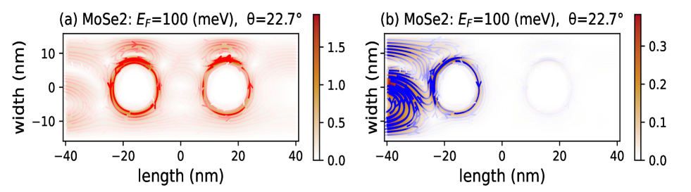
### Visual Description
# Technical Data Extraction: MoSe2 Simulation Plots
This document provides a detailed technical extraction of the data and visual components from the provided image, which consists of two side-by-side heatmaps with superimposed vector streamlines.
## 1. General Metadata
* **Subject Material:** MoSe2 (Molybdenum diselenide)
* **Common Parameters:**
* $E_F$ (Fermi Energy) = 100 (meV)
* $\theta$ (Angle) = 22.7°
* **Spatial Dimensions:**
* **X-axis (length):** Range from -40 nm to 40 nm.
* **Y-axis (width):** Range from -15 nm to 15 nm (labeled markers at -10, 0, 10).
---
## 2. Component Analysis: Plot (a)
### Header and Labels
* **Title:** (a) MoSe2: $E_F$=100 (meV), $\theta$=22.7°
* **X-axis Label:** length (nm)
* **Y-axis Label:** width (nm)
### Color Scale (Legend)
* **Location:** Right side of plot (a).
* **Type:** Sequential heatmap (White to Light Orange to Dark Red).
* **Range:** 0.0 to 1.5+ (Markers at 0.0, 0.5, 1.0, 1.5).
### Data Visualization and Trends
* **Heatmap Pattern:** Shows two distinct circular "hotspots" or rings of high intensity.
* **Ring 1 Center:** Approximately x = -18 nm, y = 0 nm.
* **Ring 2 Center:** Approximately x = +18 nm, y = 0 nm.
* **Intensity:** The highest intensity (dark red, ~1.5) is concentrated along the circumference of these two rings.
* **Streamlines:** Red vector lines with arrows indicate a clockwise flow around both circular structures. There is also a diffuse flow pattern on the far left (x = -40 to -30 nm).
---
## 3. Component Analysis: Plot (b)
### Header and Labels
* **Title:** (b) MoSe2: $E_F$=100 (meV), $\theta$=22.7°
* **X-axis Label:** length (nm)
* **Y-axis Label:** width (nm)
### Color Scale (Legend)
* **Location:** Right side of plot (b).
* **Type:** Sequential heatmap (White to Light Orange to Dark Red).
* **Range:** 0.0 to 0.3+ (Markers at 0.0, 0.1, 0.2, 0.3). Note the scale is significantly lower than plot (a).
### Data Visualization and Trends
* **Heatmap Pattern:**
* High intensity is concentrated on the far left edge (x = -40 nm) and around the first ring.
* The second ring (at x = +18 nm) shows almost zero intensity (white).
* **Streamlines:**
* **Color:** Blue vector lines.
* **Flow:** Complex turbulent/vortex-like flow on the left side (x = -40 to -25 nm).
* **Ring Interaction:** A strong clockwise circular flow is visible around the first ring (centered at x = -18 nm). Unlike plot (a), there is no significant flow or intensity around the second ring location.
* **Trend Verification:** The data series shows a rapid decay in intensity and flow magnitude as one moves from left to right across the length of the sample.
---
## 4. Comparative Summary Table
| Feature | Plot (a) | Plot (b) |
| :--- | :--- | :--- |
| **Max Intensity Value** | ~1.5+ | ~0.3+ |
| **Streamline Color** | Red | Blue |
| **Symmetry** | Roughly symmetric; both rings active. | Highly asymmetric; only left side/first ring active. |
| **Flow Direction** | Clockwise around both rings. | Clockwise around the first ring; turbulent on the left. |
| **Primary Focus** | Total field/density distribution. | Likely a specific component or current flow showing attenuation. |
## 5. Spatial Grounding and Coordinates
* **Origin [0,0]:** Located in the center of the length/width grid.
* **Ring 1 Radius:** Approximately 8 nm.
* **Ring 2 Radius:** Approximately 8 nm.
* **Legend Placement:** Both legends are vertically oriented on the right-hand side of their respective plots, spanning the full height of the y-axis.
</details>
<details>
<summary>x29.png Details</summary>
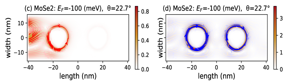
### Visual Description
# Technical Data Extraction: MoSe2 Current Density and Potential Maps
This document provides a detailed technical extraction of the data presented in the two-panel scientific visualization. The image consists of two heatmaps with overlaid vector streamlines, representing physical properties of a MoSe2 (Molybdenum diselenide) system.
## 1. General Metadata
* **Material:** MoSe2
* **Fermi Energy ($E_F$):** -100 (meV)
* **Angle ($\theta$):** 22.7°
* **Coordinate System:**
* **X-axis:** length (nm), ranging from -40 to 40.
* **Y-axis:** width (nm), ranging from -15 to 15 (labeled markers at -10, 0, 10).
---
## 2. Panel (c) Analysis
### Header Information
* **Label:** (c)
* **Title Text:** MoSe2: $E_F$=-100 (meV), $\theta$=22.7°
### Spatial Data and Trends
* **Component Isolation:** This panel displays a localized intensity field concentrated on the left side of the plot.
* **Visual Trend:** The highest intensity is located at the far left boundary (length $\approx$ -40 nm). A secondary circular feature (vortex-like) is centered at approximately length = -15 nm, width = 0 nm. The right half of the plot (length > 0 nm) shows near-zero intensity.
* **Streamlines:** Red streamlines indicate a clockwise flow around the circular feature centered at (-15, 0).
### Color Scale (Legend)
* **Location:** Right side of panel (c).
* **Type:** Sequential heatmap (White to Dark Red/Brown).
* **Range:** 0.0 to 0.8 (units not explicitly stated, likely normalized current density or local density of states).
* **Markers:** 0.0, 0.2, 0.4, 0.6, 0.8.
---
## 3. Panel (d) Analysis
### Header Information
* **Label:** (d)
* **Title Text:** MoSe2: $E_F$=-100 (meV), $\theta$=22.7°
### Spatial Data and Trends
* **Component Isolation:** This panel displays two distinct, high-intensity circular features.
* **Visual Trend:**
* **Feature 1:** A circular ring centered at approximately length = -15 nm, width = 0 nm.
* **Feature 2:** A circular ring centered at approximately length = +15 nm, width = 0 nm.
* The intensity is significantly higher than in panel (c), as indicated by the color scale.
* **Streamlines:** Blue streamlines with arrows indicate counter-clockwise flow around both circular features.
### Color Scale (Legend)
* **Location:** Right side of panel (d).
* **Type:** Sequential heatmap (White to Dark Red/Brown).
* **Range:** 0 to 3 (units not explicitly stated, likely a different physical quantity than panel c, such as magnetic field or potential).
* **Markers:** 0, 1, 2, 3.
---
## 4. Comparative Summary
| Feature | Panel (c) | Panel (d) |
| :--- | :--- | :--- |
| **Primary Focus** | Left-side boundary and one vortex | Two symmetric circular features |
| **Max Scale Value** | 0.8 | 3.0 |
| **Flow Direction** | Clockwise (Red arrows) | Counter-clockwise (Blue arrows) |
| **Vortex Centers (approx)** | (-15, 0) | (-15, 0) and (+15, 0) |
**Note on Language:** All text in the image is in English. No other languages were detected.
</details>
<details>
<summary>x30.png Details</summary>
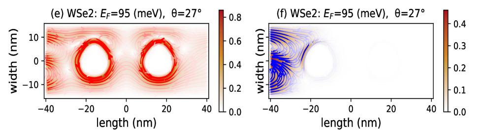
### Visual Description
# Technical Data Extraction: WSe2 Streamline and Heatmap Analysis
This document provides a detailed extraction of the data and visual components from the provided image, which consists of two side-by-side scientific plots (labeled 'e' and 'f') representing physical properties of Tungsten Diselenide ($WSe_2$).
## 1. Global Metadata and Parameters
Both plots share the same experimental/simulated parameters as indicated in their headers:
- **Material:** $WSe_2$
- **Fermi Energy ($E_F$):** $95 \text{ (meV)}$
- **Angle ($\theta$):** $27^\circ$
- **X-Axis (Length):** Range from $-40$ to $40 \text{ nm}$.
- **Y-Axis (Width):** Range from approximately $-15$ to $15 \text{ nm}$ (labeled markers at $-10, 0, 10$).
---
## 2. Plot (e) Analysis
### Header and Labels
- **Title:** (e) $WSe_2: E_F=95 \text{ (meV)}, \theta=27^\circ$
- **Y-axis Label:** width (nm)
- **X-axis Label:** length (nm)
### Component Isolation: Main Chart (e)
- **Visual Type:** Streamline plot overlaid on a heatmap.
- **Spatial Features:** Two distinct circular "voids" or regions of interest centered at approximately $x = -15 \text{ nm}$ and $x = +15 \text{ nm}$.
- **Flow Pattern:** The streamlines show a circulating or "vortex" behavior around these two centers. The flow enters from the left ($x = -40$), circulates clockwise around the first void, and continues toward the second void.
- **Color Intensity:** The highest intensity (dark red) is concentrated in the circular paths immediately surrounding the two voids.
### Color Bar / Legend (e)
- **Location:** Right side of plot (e).
- **Scale:** Linear, from $0.0$ to $0.8$.
- **Color Gradient:** White (0.0) $\rightarrow$ Light Orange $\rightarrow$ Dark Red (0.8).
- **Trend:** The data shows high density/magnitude (0.6 to 0.8) in the rings around the voids and lower density (0.0 to 0.2) in the far-field regions (edges of the plot).
---
## 3. Plot (f) Analysis
### Header and Labels
- **Title:** (f) $WSe_2: E_F=95 \text{ (meV)}, \theta=27^\circ$
- **Y-axis Label:** width (nm)
- **X-axis Label:** length (nm)
### Component Isolation: Main Chart (f)
- **Visual Type:** Streamline plot with directional color coding.
- **Spatial Features:** Similar geometry to plot (e) with two circular regions, but the data is heavily concentrated on the left side of the plot.
- **Flow Pattern:**
- High-density streamlines originate at the left boundary ($x = -40$).
- The streamlines are colored blue and dark red.
- The flow appears to "hit" the first void at $x = -15$ and dissipate or terminate.
- The right half of the plot ($x > 0$) is almost entirely white/empty, indicating near-zero values.
- **Trend Verification:** Unlike plot (e) which shows symmetric activity around both voids, plot (f) shows a sharp decay in magnitude as the length increases from left to right.
### Color Bar / Legend (f)
- **Location:** Right side of plot (f).
- **Scale:** Linear, from $0.0$ to $0.4$. Note that the maximum scale is half that of plot (e).
- **Color Gradient:** White (0.0) $\rightarrow$ Orange $\rightarrow$ Dark Red (0.4).
- **Note on Blue Lines:** While the color bar shows a red gradient, the plot contains blue streamlines. In scientific visualization, this often represents a negative value or a specific vector component not explicitly defined in the color bar, or a "cool-to-warm" map where blue is the opposite phase of red.
---
## 4. Comparative Summary Table
| Feature | Plot (e) | Plot (f) |
| :--- | :--- | :--- |
| **Max Value (Color Bar)** | 0.8 | 0.4 |
| **Spatial Distribution** | Bimodal (Active around both voids) | Unimodal (Active only near left boundary) |
| **Symmetry** | Roughly symmetric across $x=0$ | Highly asymmetric; decays toward the right |
| **Primary Feature** | Circulating vortices around both centers | Injection/Scattering at the first center |
## 5. Text Transcription Summary
- **Text Elements:** "width (nm)", "length (nm)", "(e) WSe2: Ef=95 (meV), $\theta$=27°", "(f) WSe2: Ef=95 (meV), $\theta$=27°".
- **Axis Markers (X):** -40, -20, 0, 20, 40.
- **Axis Markers (Y):** -10, 0, 10.
- **Color Bar Markers (e):** 0.0, 0.2, 0.4, 0.6, 0.8.
- **Color Bar Markers (f):** 0.0, 0.1, 0.2, 0.3, 0.4.
</details>
<details>
<summary>x31.png Details</summary>
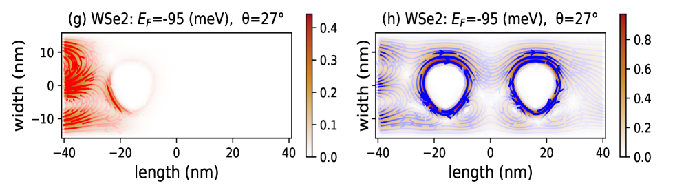
### Visual Description
# Technical Data Extraction: WSe2 Current Density and Flow Maps
This document provides a detailed technical extraction of the data contained in the provided image, which consists of two side-by-side scientific plots (labeled 'g' and 'h') representing physical simulations of Tungsten Diselenide ($WSe_2$).
## 1. General Metadata
* **Material:** $WSe_2$ (Tungsten Diselenide)
* **Fermi Energy ($E_F$):** -95 meV
* **Angle ($\theta$):** 27°
* **Primary Language:** English
---
## 2. Component Isolation: Plot (g)
### Header & Labels
* **Title:** (g) $WSe_2$: $E_F$=-95 (meV), $\theta$=27°
* **Y-axis Label:** width (nm)
* **X-axis Label:** length (nm)
### Axis Scales
* **X-axis Range:** -40 to 40 nm (Markers at -40, -20, 0, 20, 40)
* **Y-axis Range:** -10 to 10 nm (Markers at -10, 0, 10)
### Colorbar (Legend)
* **Location:** Right side of plot (g)
* **Scale:** 0.0 to 0.4 (Linear gradient from white/light orange to dark red)
* **Function:** Represents magnitude (likely current density or local density of states).
### Data Content & Trends
* **Visual Trend:** The data is concentrated on the left side of the plot (negative length). The right side (length > -10 nm) is largely empty/white, indicating zero or near-zero values.
* **Flow Features:**
* There is a high-intensity region (dark red, ~0.4 on the scale) between length -40 and -25 nm.
* Streamlines (red lines) show a turbulent or circulating flow pattern on the far left.
* A distinct "void" or circular exclusion zone is visible centered approximately at length = -15 nm, width = 0 nm.
* A high-intensity "boundary" (dark red) wraps around the left edge of this void.
---
## 3. Component Isolation: Plot (h)
### Header & Labels
* **Title:** (h) $WSe_2$: $E_F$=-95 (meV), $\theta$=27°
* **Y-axis Label:** width (nm)
* **X-axis Label:** length (nm)
### Axis Scales
* **X-axis Range:** -40 to 40 nm (Markers at -40, -20, 0, 20, 40)
* **Y-axis Range:** -10 to 10 nm (Markers at -10, 0, 10)
### Colorbar (Legend)
* **Location:** Right side of plot (h)
* **Scale:** 0.0 to 0.8 (Linear gradient from white/light orange to dark red)
* **Note:** The scale in (h) is double the magnitude of the scale in (g).
### Data Content & Trends
* **Visual Trend:** Unlike plot (g), the data in (h) spans the entire length of the channel (-40 to 40 nm).
* **Flow Features:**
* **Vortex Structures:** There are two prominent circular "voids" or obstacles centered at approximately **length = -18 nm** and **length = +18 nm**.
* **Circulation:** Blue streamlines with arrows indicate a strong clockwise circulation around these two centers.
* **Intensity:** The highest intensity (dark red, ~0.8) occurs at the immediate boundaries of these circular structures.
* **Background Flow:** Between the vortices and at the far left/right edges, the flow appears more laminar but contains smaller secondary eddies.
* **Symmetry:** The plot shows a high degree of periodicity or symmetry relative to the length = 0 axis.
---
## 4. Comparative Analysis
| Feature | Plot (g) | Plot (h) |
| :--- | :--- | :--- |
| **Max Magnitude** | 0.4 | 0.8 |
| **Spatial Coverage** | Left-heavy (localized) | Full channel (distributed) |
| **Primary Features** | Single partial vortex/boundary | Two complete counter-circulating vortices |
| **Streamline Color** | Red | Blue (with directional arrows) |
**Summary:** These plots likely represent different components of a current or wave function (e.g., longitudinal vs. transverse or different valley contributions) for $WSe_2$ under specific energy and angular conditions. Plot (h) shows a much more developed and higher-magnitude flow pattern compared to the localized behavior in plot (g).
</details>
<details>
<summary>x32.png Details</summary>
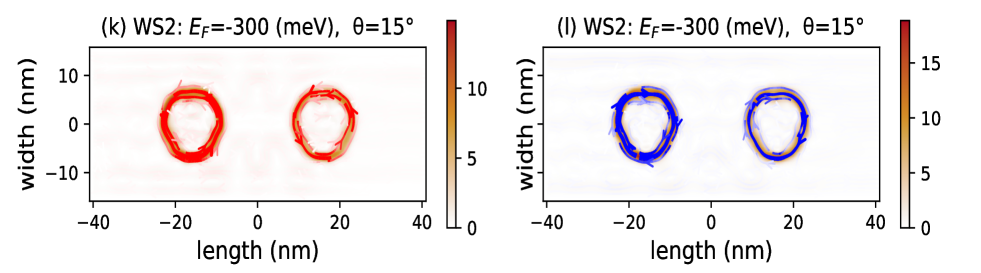
### Visual Description
# Technical Data Extraction: WS2 Simulation Heatmaps
This document provides a detailed technical extraction of the data presented in the two-panel scientific visualization. The image consists of two heatmaps, labeled (k) and (l), representing physical properties of a $WS_2$ (Tungsten Disulfide) system.
## 1. General Metadata and Global Parameters
Both panels share the following experimental/simulation parameters:
* **Material:** $WS_2$
* **Fermi Energy ($E_F$):** $-300 \text{ meV}$
* **Angle ($\theta$):** $15^\circ$
* **Y-Axis Label:** width (nm)
* **X-Axis Label:** length (nm)
* **Y-Axis Scale:** $-10$ to $10$ (with ticks at $-10, 0, 10$)
* **X-Axis Scale:** $-40$ to $40$ (with ticks at $-40, -20, 0, 20, 40$)
---
## 2. Panel (k) Analysis
### Header Information
* **Label:** (k)
* **Title:** $WS_2: E_F = -300 \text{ (meV)}, \theta = 15^\circ$
### Component Isolation: Main Chart (k)
* **Visual Trend:** The heatmap shows two distinct ring-like structures centered at approximately $x = -15 \text{ nm}$ and $x = +15 \text{ nm}$ along the $y = 0$ axis.
* **Vector Overlay:** Red arrows are superimposed on the rings.
* **Directionality:** The arrows indicate a **clockwise** circulation pattern in both the left and right rings.
* **Intensity Distribution:** The highest intensity (darkest red/orange) is concentrated along the perimeter of the rings, forming a circular "track."
### Component Isolation: Legend/Color Bar (k)
* **Spatial Placement:** Right side of panel (k).
* **Scale:** Linear, from $0$ to $15$.
* **Ticks:** $0, 5, 10$. (The top of the bar extends toward $15$).
* **Color Gradient:** White (0) $\rightarrow$ Light Orange $\rightarrow$ Dark Red/Brown (15).
---
## 3. Panel (l) Analysis
### Header Information
* **Label:** (l)
* **Title:** $WS_2: E_F = -300 \text{ (meV)}, \theta = 15^\circ$
### Component Isolation: Main Chart (l)
* **Visual Trend:** Similar to panel (k), this chart features two ring-like structures at $x \approx \pm 15 \text{ nm}$.
* **Vector Overlay:** Blue arrows are superimposed on the rings.
* **Directionality:** The arrows indicate a **counter-clockwise** circulation pattern in both the left and right rings. This is the primary differentiator from panel (k).
* **Intensity Distribution:** The background heatmap (orange/red) appears identical in intensity and spatial distribution to panel (k), suggesting the underlying scalar field is the same, while the vector field (blue arrows) represents a different component or state (e.g., opposite spin or valley).
### Component Isolation: Legend/Color Bar (l)
* **Spatial Placement:** Right side of panel (l).
* **Scale:** Linear, from $0$ to $15$.
* **Ticks:** $0, 5, 10, 15$.
* **Color Gradient:** White (0) $\rightarrow$ Light Orange $\rightarrow$ Dark Red/Brown (15).
---
## 4. Comparative Summary
| Feature | Panel (k) | Panel (l) |
| :--- | :--- | :--- |
| **Ring Centers** | $\approx \pm 15 \text{ nm}$ | $\approx \pm 15 \text{ nm}$ |
| **Vector Color** | Red | Blue |
| **Circulation** | Clockwise | Counter-clockwise |
| **Max Intensity** | $\approx 12-14$ (on 0-15 scale) | $\approx 12-14$ (on 0-15 scale) |
| **Background** | White/Neutral | White/Neutral |
**Technical Conclusion:** The images depict localized electronic or magnetic states in a $WS_2$ nanostructure. The two panels likely represent time-reversal symmetric partners or different valley/spin polarizations, as evidenced by the identical spatial intensity of the rings but perfectly inverted circulation directions (clockwise red vs. counter-clockwise blue).
</details>
Figure 10: Real-space profiles for both valley currents: red (blue) lines show the current profile from states originating in valley ${\bf K_{1}}\quad({\bf K_{2}}$ ). Panels (a)-(d) show the valley conductance vs twist angle $\theta$ for IQDs made of MoSe 2 on graphene at $E_{F}=± 100$ meV. Panels (e)-(h) are for WSe 2 on graphene at $E_{F}=± 95$ meV. Panels in (k) and (l) correspond to WS 2 at higher energy $E_{F}=-300$ meV.
IV Conclusions and summary
We have used a tight-binding approach to obtain an effective, low-energy Hamiltonian to investigate valley-dependent transport through an array of proximity-induced quantum dots with $C_{3v}$ symmetry in a zigzag graphene nanoribbon. The model is a natural extension of the structure studied in Ref. [51] that analyzed spin and charge distributions in a graphene quantum dot induced by a WSe 2 island. Because the fabrication of graphene/TMD heterostructures with quantum dots of one or the other material is rapidly evolving [52, 53, 54], experimental implementations for arrays of quantum dots will likely be realized in the near future.
Our results show that the valley conductance exhibits an interesting behavior sensitive to the model parameters and the values of the various SOCs induced by the islands that decorate the ribbon. At the same time, this sensitivity is a great advantage for monitoring and controlling the different valley filter regimes observed. The results reveal the localization of valley-centered states produced by the competition between Zeeman and Rashba couplings in narrow IQDs. For larger IQDs, the valley states combine with bulk states, and the valley polarization is considerably deteriorated [34].
Following Ref. [30], the qualitative description of the model shows that by varying Zeeman couplings, the conductance through a symmetric chain of quantum dots displays square-shaped curves with wide gaps. However, these features tend to vanish for some large ISOC values with the subsequent vanishing of valley polarization. Furthermore, for specific ranges of ISOC values, both valleys are present, implying that the device does not display a perfect valley-transistor behavior. An important conclusion from the qualitative description is the similarity of this system to the Datta-Das transistor. In both cases, the spin conductance is directly controlled by the strength of the Rashba SOC. In this respect, the most important SOC for good valley polarization is the staggered intrinsic SOC. These features could be helpful for further exploration of actual devices.
The sensitivity to the Rashba coupling is discussed in the presence of weak ISOC to describe realistic settings where proximity effects develop. The valley conductance shows that tuning the valley polarization and switching the valley scattering in the system using a top gate is possible. The possibility of using TMDs as decorating islands to form IQDs has also been discussed. We have shown that the presence of the PIA coupling, characteristic of these structures, does not affect the valley-polarization. Therefore, such islands can be used to tune the polarization by either strain or twists since the Rashba and Zeeman coupling are sensitive to external electric or strain field effects [28, 46, 47].
Finally, we have applied these models to solve examples of realistic material combinations. To give a comprehensive picture, we have used graphene/TMD heterostructures with different semiconducting materials: MoS 2, MoSe 2, WSe 2, and WS 2. We noticed that IQDs based on semiconducting TMDs might be used as promising islands for generating valley Hall signals. Indeed, TMDs allow valley filtering processes and break the valley degeneracy, producing a valley-polarized current that favors valley selection by tuning the sign of the incident Fermi energy or the value of twist angles. Notably, the TMD island and control of the twisting angle allow various options (as they determine different values of ISOCs) to monitor valley-driven currents, confine both valley states simultaneously in the same region, or split the valley confinement states.
Achieving a nearly square-wave transmission and a valley-valve effect for the ${\bf K_{1}}$ or ${\bf K_{2}}$ valleys is highly desirable for device applications. Moreover, the confinement of quasi-bound states from either valley is extremely important for manipulating optoelectronic interactions [13, 23, 55] and valley-qubit systems [17, 3, 56]. Furthermore, the mechanism for generating valley-Hall conductivity with valley-neutral currents could be handy to obtain pure valley-Hall signals. The system proposed in this manuscript exhibits features close to these goals; however, asymmetric QDS with controlled shape and several induced point group symmetries could lead to richer results. We plan to address this issue in future work.
Acknowledgements. The authors acknowledge computing time on the SHAHHEN supercomputers at KAUST University, Saudi Arabia, and the supercomputers at the Centre for Research in Molecular Modeling (CERMM), Richard J. Renaud Science Complex, Concordia University. AB would like to thank Dr. Adel Abbout at KFUPM, Saudi Arabia, for helpful discussions.
Appendix A Valley-dependent conductance
As stated, we use the scattering matrix formalism to calculate the individual valley conductances. We separate the propagating modes in the leads depending on their velocity and momentum direction using the Kwant package [40]. In the scattering region, valley currents might be mixed due to inter-valley scattering. However, as the two valleys are far apart in the Brillouin zone, effective valley mixing will require short-range potentials. A graphene membrane wraps smoothly for graphene deposited on top of islands to minimize strain effects. Thus, the sharp atomic termination of the island (that could give rise to inter-valley mixing) is effectively masked. These issues will have a negligible contribution for islands on top of graphene if the islands and their separation are large enough [57].
To this end, we consider only propagating states for which $\Phi({\bf vF}>0)$ . The applied source-drain voltage chooses the direction of the current composed of these states, which have both spin and valley degrees of freedom. We focus first on the valley degree and lift the valley degeneracy by defining the propagating wave functions $\Phi_{\bf K_{1}}=\Phi({\bf k}>0),\Phi_{\bf K_{2}}=\Phi({\bf k}<0)$ .
These wave functions independently solve the scattering problem in the reciprocal space. To implement the Green’s function formalism [39] we need to include the scattering matrices $S^{mn}=S_{\bf K_{1}}^{mn}+S_{\bf K_{2}}^{mn}$ with $S_{\bf K_{1,2}}^{mn}$ given by
$$
S_{\bf K_{1,2}}^{m,n}=\text{Tr}[G_{\bf K_{1,2}}\Gamma^{m}\,G^{\dagger}_{\bf K_%
{1,2}}\,\Gamma^{n}],\qquad(m,n=L,R\ or\ R,L);
$$
The Green’s function and $\Gamma$ matrices are given by
$$
\displaystyle G(\epsilon,{\bf K_{1,2}}) \displaystyle= \displaystyle\left[\left(\epsilon+i\eta\right)I-H_{QD}({\bf K_{1,2}})-\Sigma%
\right]^{-1} \displaystyle\Gamma \displaystyle= \displaystyle i(\Sigma-\Sigma^{\dagger}).
$$
$\Gamma$ defines the self-energy of the contacts placed to the left and right of the scattering region, and the relevant Hamiltonian is $H_{QD}$ , cf. Eq. (1). Then, for each valley mode, the valley conductance at the Dirac cones is given by Eq. (2).
Appendix B Valley-resolved current
To obtain the local density of states (LDOS) and currents per valley, we obtain the wave functions of the propagating modes $\Phi$ for a given energy $E$ and site $i$ . The propagating wave functions are stored per site depending on their momentum $\left\{\Phi({\bf K_{1}}),\ \Phi({\bf K_{2}})\right\}$ and their spin degree of freedom. The resulting LDOS, at a given site $i$ in the sample, is defined by
$$
\text{LDOS}^{\bf K_{1,2}}\left(E,i\right)=\sum_{l}\left|\langle i|\Phi^{\bf K_%
{1,2}}_{l}\rangle\right|^{2}\delta(E-E_{l})
$$
where the sum is over all electron eigenstates $|\Phi_{l}\rangle=c_{l}^{\dagger}|0\rangle$ of the Hamiltonian $H_{QD}$ in Eq. (1) with energy $E_{l}$ . The valley-resolved LDOS in Eq. (B.1) is calculated using Chebyshev polynomials [58] and damping kernels [59].
The corresponding density operator and the continuity equation are expressed as
$$
\rho_{q}^{\bf K_{1,2}}=\sum_{a}[\Phi_{a}^{\bf K_{1,2}}]^{*}\,H^{s}_{q}\,\Phi_{%
a}^{\bf K_{1,2}},\qquad\frac{\partial\rho_{a}^{\bf K_{1,2}}}{\partial t}-\sum_%
{b}J_{a,b}^{\bf K_{1,2}}=0.
$$
where $a$ refers to all sites in the scattering region, $J_{ab}^{\bf K_{1,2}}$ is the valley-resolved current, and $H^{s}_{q}$ is the $q$ -Fourier component of the hopping term in the scattering region.
For a given site density $\rho_{a}$ , we sum over all the neighboring sites $b$ . As a result, the valley current $J^{{\bf K_{1,2}}}_{ab}$ takes the form
$$
J_{a,b}^{\bf K_{1,2}}=[\Phi^{\bf K_{1,2}}({\bf v>0})]^{*}\left(i\sum_{\gamma}H%
^{*}_{ab\gamma}H^{s}_{a\gamma}-H^{s}_{a\gamma}H_{ab\gamma}\right)[\Phi^{\bf K_%
{1,2}}({\bf v>0})]
$$
where $H_{ab\gamma}$ is a component of a rank-4 tensor that can be represented as a vector of matrices, and $\gamma$ is an index that runs over sites in real space. In this expression, Latin indices go over sites, and Greek indices run over the degrees of freedom in the Hilbert space. For more details about obtaining the current operator, see references [49, 29, 48, 40].
References
References
- [1] N. Rohling and G. Burkard, New Journal of Physics 14, 083008 (2012).
- [2] J. R. Schaibley, H. Yu, G. Clark, P. Rivera, J. S. Ross, K. L. Seyler, W. Yao, and X. Xu, Nature Reviews Materials 1, 16055 (2016).
- [3] G. Szechenyi, L. Chirolli, and A. Palyi, 2D Materials 5, 035004 (2018).
- [4] D. Culcer, A. L. Saraiva, B. Koiller, X. Hu, and S. Das Sarma, Phys. Rev. Lett. 108, 126804 (2012).
- [5] E. A. Laird, F. Pei, and L. P. Kouwenhoven, Nature nanotechnology 8, 565 (2013).
- [6] N. Hadadi, A. Belayadi, A. AlRabiah, O. Ly, C. A. Akosa, M. Vogl, H. Bahlouli, A. Manchon, and A. Abbout, Phys. Rev. B 108, 195418 (2023).
- [7] L. A. Benitez , J. F. Sierra , W. S. Torres , A. Arrighi, F. Bonell, M. V. Costache and S. O. Valenzuela. Nature Physics 14, 303 (2018).
- [8] Y. K. Luo, J. Xu, T. Zhu, G Wu, E. J. McCormick, W. Zhan, M. R. Neupane, R. K. Kawakami, Nano Lett 6, 3877 (2017).
- [9] V. Bonbien, F. Zhuo, A. Salimath, O. Ly, A. Abbout and A. Manchon, J. Phys. D. Appl. Phys. 55, 103002 (2022).
- [10] D. Xiao, G. B. Liu, W. Feng, X. Xu, and W. Yao, Phys. Rev. Lett. 108, 196802 (2012).
- [11] J. Qi, X. Li, Q. Niu, and J. Feng, Phys. Rev. B 92, 121403(R) (2015).
- [12] A. Cresti, B. K. Nikolic, J. H. García, and S. Roche, Riv. del Nuovo Cim. 39, 587 (2016).
- [13] Z. Zhang, X. Ni, H. Huang, L. Hu, and F. Liu, Phys. Rev. B 99, 115441 (2019).
- [14] A.Krasnok, and A. Alù, Appl. Sci. 7, 1157 (2018).
- [15] S. Sharma, P. Elliott, and S. Shallcross, Optica 9, 947 (2022).
- [16] R. H. Godiksen, S. Wang, T. V. Raziman, J. G. Rivas and A. G. Curto, Nanoscale 14, 17761 (2022).
- [17] Y. Wu, Q. Tong, G-B. Liu, H. Yu and W. Yao, Phys. Rev. B 93, 045313 (2016).
- [18] P. A. Maksym and H. Aoki, Phys. Rev. B 88, 081406(R) (2013).
- [19] A. Orlof, A. A. Shylau and I. Zozoulenko, Phys. Rev. B 92, 075431 (2015).
- [20] W. A. Behn, Z. J. Krebs, K. J. Smith, K. Watanabe, T. Taniguchi, and V. W. Brar, Nano Lett 21, 5013 (2021).
- [21] SY. Li and L. He, Front. Phys. 17, 33201 (2022).
- [22] T. Cao, G. Wang, W. Han, H. Ye, C. Zhu, J. Shi, Q. Niu, P. Tan, E. Wang, B. Liu, Nature communications 3, 887 (2012).
- [23] T. Aktor, J. H. Garcia, S. Roche, A-P. Jauho, and S. R. Power, Phys. Rev. B 103, 115406 ( 2021).
- [24] Y. Iwasa, in JSAP-OSA Joint Symposia 2015 Abstracts, (Optica Publishing Group, 2015), p. $15p_{2}D_{1}$ .
- [25] Md.T Mahmud and N. Sandler, Phys. Rev. B 102, 235410 (2020).
- [26] F. Solomon and S. R. Power, Phys. Rev. B 103, 235435 (2021).
- [27] D. Kochan, S. Irmer, and J. Fabian, Phys. Rev. B 95, 165415(2017).
- [28] M. Gmitra, D. Kochan, P. Hagl, and J. Fabian, Phys. Rev. B 93, 155104 (2016).
- [29] A. Belayadi and P. Vasilopoulos, Nanotechnology 34, 085704 (2023).
- [30] C. L. Kane and E. J. Mele, Phys. Rev. Lett. 95, 226801 (2005).
- [31] M. Gmitra and J. Fabian, Phys. Rev. B 92, 155403 (2015).
- [32] Z. Wang, D.-K. Ki, H. Chen, H. Berger, A. H. MacDonald, and A. F. Morpurgo, Nat. Commun. 6, 8339 (2015).
- [33] Aron W. Cummings, Jose H. Garcia, Jaroslav Fabian, and Stephan Roche Phys. Rev. Lett. 119, 206601 (2017).
- [34] T. Frank, P. H $\ddot{o}$ gl, M. Gmitra, D. Kochan, and J. Fabian Phys. Rev. Lett. 120, 156402 (2018).
- [35] T. Naimer, K. Zollner, M. Gmitra, and L. Fabian, Phys. Rev. B 104, 195156 (2021).
- [36] P. Hogl, T. Frank, K. Zollner, D. Kochan, M. Gmitra, and J. Fabian, Phys. Rev. Lett. 124, 136403 (2020)
- [37] F. D. M. Haldane, Phys. Rev. Lett. 61, 2015 (1988).
- [38] T. S. Ghiasi, J. Ingla-Ays, A. A. Kaverzin, and B. J. van Wees, Nano Lett. 17, 7528 32 (2017).
- [39] S. Datta, Electronic Transport in Mesoscopic Systems (Cambridge University Press, Cambridge, 1995).
- [40] C. W. Groth, M. Wimmer, A. R. Akhmerov, X. Waintal, New J. Phys. 16, 063065 (2014).
- [41] J. H. Garcia and T. G. Rappoport, 2D Materials, 3, 024007 (2016).
- [42] T. P. Cysne, J. H. Garcia, A. R. Rocha, and T. G. Rappoport, Phys. Rev. B 97, 085413 (2018).
- [43] N. Myoung, J.-W. Ryu, H.C. Park, S.J. Lee, S. Woo, Phys. Rev. B 100, 045427 (2019).
- [44] H. C. Park, M. Son, S. J. Lee, N. Myoung, Journal of the Korean Physical Society 78, 1208-1214 (2021).
- [45] K. Zollner, M. Gmitra, and J. Fabian, Phys. Rev. B 99, 125151 (2019).
- [46] Li Y and Koshino M Phys. Rev. B 99, 075438 (2019).
- [47] David A, Rakyta P, Kormanyos A, and Burkard G Phys. Rev. B 100, 085412 (2019).
- [48] A. Belayadi and P. Vasilopoulos, Nanotechnology 34, 365706 (2023).
- [49] A. Belayadi, N. A. Hadadi, P. Vasilopoulos, and A. Abbout Phys. Rev. B 108, 085419 (2023).
- [50] E. Sie, J. McIver, Y. H. Lee, F. Liang, K. Jing, and G. Nuh, Nature Mater 14, 290-294 (2015).
- [51] H-Y. Ren, Y-N. Ren, Q. Zheng, J-Q. He and L. He, Phys. Rev. B 108, L081408 (2023).
- [52] A. Manikandan, Y-Z. Chen, Ch-Ch. Shen, Ch-W. Sher, H-Ch. Kuo and Y-L. Chueh, Progress in Quantum Electronics 68, 100226 (2019).
- [53] K. J. Singh, T. Ahmed, P. Gautam, A. S. Sadhu, D-H. Lien, S-Ch. Chen, Y-L. Chueh and H-Ch. Kuo, Nanomaterials 11, 1549 (2021).
- [54] A. Alfieri, S. B. Anantharaman, H. Zhang and D. Jariwala, Advanced Materials 35, 2109621 (2022).
- [55] S. A. Vitale, D. Nezich, J. O. Varghese, P. Kim, N. Gedik, P. Jarillo-Herrero, and M. Rothschild, Small 14, 1801483 (2018).
- [56] J. Pawlowski, New J. Phys. 21 123029 (2019).
- [57] J. G. Nedell, J. Spector, A. Abbout, M. Vogl, and G. A. Fiete, Phys. Rev. B 105, 075425 (2022).
- [58] A. Ferreira and E. Mucciolo, Phys. Rev. Lett 115, 106601 (2015).
- [59] A. Weibe, G. Wellein, A. Alvermann, and H. Fehske, Rev. Mod. Phys 78, 275 (2006).