## Analog Alchemy: Neural Computation with In-Memory Inference, Learning and Routing
Dissertation zur
Erlangung der naturwissenschaftlichen Doktorwürde
(Dr. sc. UZH ETH Zürich) vorgelegt der Mathematisch-naturwissenschaftlichen Fakultät der Universität Zürich und der Eidgenössischen Technischen Hochschule Zürich von
Yiğit Demirağ
aus der
Türkei
Promotionskommission
Prof. Dr. Giacomo Indiveri (Vorsitz und Leitung)
Prof. Dr. Melika Payvand Prof. Dr. Benjamin Grewe
Zürich, 2024
## yigit demirag
## ANALOG ALCHEMY: NEURAL COMPUTATION WITH IN-MEMORY I N F E R E N C E , LEARNING AND ROUTING
To the engineers and scientists who will one day build superintelligence; from whatever materials and circuits, in whatever form.
## ABSTRACT
As neural computation is revolutionizing the field of Artificial Intelligence (AI), rethinking the ideal neural hardware is becoming the next frontier. Fast and reliable von Neumann architecture has been the hosting platform for neural computation. Although capable, its separation of memory and computation creates the bottleneck for the energy efficiency of neural computation, contrasting the biological brain. The question remains: how can we efficiently combine memory and computation, while exploiting the physics of the substrate, to build intelligent systems? In this thesis, I explore an alternative way with memristive devices for neural computation, where the unique physical dynamics of the devices are used for inference, learning and routing. Guided by the principles of gradient-based learning, we selected functions that need to be materialized, and analyzed connectomics principles for efficient wiring. Despite non-idealities and noise inherent in analog physics, I will provide hardware evidence of adaptability of local learning to memristive substrates, new material stacks and circuit blocks that aid in solving the credit assignment problem and efficient routing between analog crossbars for scalable architectures. First, I address limited bit precision problem in binary Resistive Random Access Memory (RRAM) devices for stable training. By introducing a new device programning technique that precisely controls the filament growth process, we enhance the effective bit precision of these devices. Later, we prove the versatility of this technique by applying it to novel perovskite memristors. Second, I focus on the hard problem of online credit assignment in recurrent Spiking Neural Networks (SNNs) in the presence of memristor non-idealities. I present a simulation framework based on a comprehensive statistical model of Phase Change Material (PCM) crossbar array, capturing all major device non-idealities. Building upon the recently developed e-prop local learning rule, we demonstrate that gradient accumulation is crucial for reliably implementing the learning rule with memristive devices. Moreover, I introduce PCM-trace, a scalable implementation of synaptic eligibility traces, a functional block demanded by many learning rules, using volatile characteristics by specifically fabricated PCM devices. Third, I present our discovery of a novel memristor material capable of switching between volatile and non-volatile modes. This reconfigurable memristor, based on halide perovskite nanocrystals, offers a significant advancement in emerging memory technologies, enabling the implementation of both static and dynamic neural variables with the same material and fabrication technique, while holding the world record in endurance. Finally, I introduce Mosaic, a memristive systolic architecture for in memory computing and routing. Mosaic, trained with our novel layout-aware training methods, efficiently implements small-world graph connectivity and demonstrates superior energy efficiency in spike routing compared to other hardware platforms.
## ACKNOWLEDGEMENTS
This thesis wouldn't have been possible without many people: scientists, friends, and family. I'm honored to have shared this journey with such curious and driven individuals. Among the many who contributed, there are a few exceptional individuals who were absolutely core to making this happen:
First I'd like to thank my supervisor, Giacomo Indiveri, who is a rare scientist truly channeling his work towards a dream. Over these 5 years, he gave me complete freedom to explore what I believe are the most exciting problems, while providing me with high-bandwidth feedback on demand, with more than 500 emails and many thousands of DMs. He taught me the importance of pushing unusual ideas to the limit. Whenever I came up with an ambitious project goal, he always reminded me to deeply consider the efficiency on the silicon, first. I'm grateful for having been his student.
I've been very fortunate to coincide with Melika Payvand, my co-supervisor, in this particular academic space and time. She is the most curious mind craving to understand the emergence of intelligence from the physics of computation, and her passion is infectious. Together, we traversed the probability trees for nearly every projects in my PhD, and executed against the entropy. Her close friendship is the cherry on the cake; I enjoyed and valued every second of it.
Then there are people I am very lucky to collaborate with and learn from. Rohit A. John, an extraordinary person who taught me the importance of grinding with massive focus while solving hard problems. And Elisa Vianello, who always provided her seamless support and insights that have made hard projects a joyful exploration. And Emre Neftci, whose disruptive scientific ideas deeply resonated with me, and with whom I always enjoyed discussing ideas.
I have to thank Alpha, Anqchi, Arianna, Chiara, Dmitrii, Farah, Filippo, Jimmy, Karthik, Manu, Maryada, Nicoletta, Tristan, and many others, who I hope will forgive me for not being mentioned individually or for resorting to alphabetical order when I did. Thank you for inspiring conversations in INI hallways, night walks in Zurich, and giving me the privilege of calling you, my friends.
During my PhD, I completed two internships at Google Zurich and one research visit at MILA. All of these were fantastic learning experiences, where I got a chance to reshape my research scope. From these experiences, I would especially like to thank Jyrki Alakuijala, Johannes von Oswald, Eyvind Niklasson, Ettore Randazzo, Alexander Mordvintsev, Esteban Real, Arna Ghosh, Jonathan Cornford, Joao Sacramento, Blake Richards, Guillaume Lajoie, and Blaise Aguera y Arcas.
I would also like to extend my thanks to my professors from my Master's degree, particularly Ekmel Ozbay, Bayram Butun and Yusuf Leblebici, for their invaluable support and inspiration.
And to Gizay, for sharing most of the journey and everything we created together.
But most of all, I want to express my deepest gratitude to my mom and dad, who inspired me to be curious, to take the world as a playground, and provided me with a loving home. And to my little brother, Efe, who is the best teammate in every game we play and in life's adventures.
## CONTENTS
| 1 Introduction | 1 Introduction | 1 Introduction | 1 Introduction | 1 | 1 | 1 | 1 | 1 |
|------------------|-----------------------------------------------------------------------------------|----------------------------------------------------------------------------------|-----------------------------------------------------------------------------------|-----------------------------------------------------------------------------------|-----------------------------------------------------------------------------------|-----------------------------------------------------------------------------------|-----|-----|
| 2 | Enhancing Bit Precision of Binary Memristors for Robust On-chip Learning | Enhancing Bit Precision of Binary Memristors for Robust On-chip Learning | Enhancing Bit Precision of Binary Memristors for Robust On-chip Learning | Enhancing Bit Precision of Binary Memristors for Robust On-chip Learning | Enhancing Bit Precision of Binary Memristors for Robust On-chip Learning | 9 | 9 | |
| | 2 . 1 | Introduction 9 | Introduction 9 | Introduction 9 | Introduction 9 | Introduction 9 | | |
| | 2 . 2 | ReRAM Device Modeling 10 | ReRAM Device Modeling 10 | ReRAM Device Modeling 10 | ReRAM Device Modeling 10 | ReRAM Device Modeling 10 | | |
| | 2 . 3 | Bit-Precision Enhancing Weight Update Rule 10 | Bit-Precision Enhancing Weight Update Rule 10 | Bit-Precision Enhancing Weight Update Rule 10 | Bit-Precision Enhancing Weight Update Rule 10 | Bit-Precision Enhancing Weight Update Rule 10 | | |
| | 2 . 4 | Learning Circuits and Architecture 12 | Learning Circuits and Architecture 12 | Learning Circuits and Architecture 12 | Learning Circuits and Architecture 12 | Learning Circuits and Architecture 12 | | |
| | 2 . 5 | System-level Simulations 13 | System-level Simulations 13 | System-level Simulations 13 | System-level Simulations 13 | System-level Simulations 13 | | |
| | 2 . 6 | Discussion 14 | Discussion 14 | Discussion 14 | Discussion 14 | Discussion 14 | | |
| 3 | Online Temporal Credit Assignment with Non-volatile and Volatile Memristors | Online Temporal Credit Assignment with Non-volatile and Volatile Memristors | Online Temporal Credit Assignment with Non-volatile and Volatile Memristors | Online Temporal Credit Assignment with Non-volatile and Volatile Memristors | Online Temporal Credit Assignment with Non-volatile and Volatile Memristors | Online Temporal Credit Assignment with Non-volatile and Volatile Memristors | 15 | |
| | 3 . 1 | Framework for Online Training of RSNNs with Non-volatile Memristors | Framework for Online Training of RSNNs with Non-volatile Memristors | Framework for Online Training of RSNNs with Non-volatile Memristors | Framework for Online Training of RSNNs with Non-volatile Memristors | 15 | 15 | |
| | | 3 . 1 . 2 | Introduction 15 Building blocks for training on in-memory processing cores | Introduction 15 Building blocks for training on in-memory processing cores | 16 | | | |
| | | 3 . 1 . 3 | PCM device modeling and integration into neural networks | PCM device modeling and integration into neural networks | 16 | | | |
| | | 3 . 1 . 4 | Discussion 23 | Discussion 23 | Discussion 23 | | | |
| | 3 . 2 | Implementing Online Training of RSNNs on a Neuromorphic Hardware | Implementing Online Training of RSNNs on a Neuromorphic Hardware | Implementing Online Training of RSNNs on a Neuromorphic Hardware | Implementing Online Training of RSNNs on a Neuromorphic Hardware | 25 | 25 | |
| | | 3 . 2 . 1 | 3 . 2 . 1 | 3 . 2 . 1 | 3 . 2 . 1 | 3 . 2 . 1 | | |
| | | 3 2 2 | From the simulation to an analog chip 25 | From the simulation to an analog chip 25 | From the simulation to an analog chip 25 | From the simulation to an analog chip 25 | | |
| | | . . | Discussion 26 | Discussion 26 | Discussion 26 | Discussion 26 | | |
| | 3 . 3 Scalable Synaptic Eligibility Traces with Volatile Memristive Devices 28 | 3 . 3 Scalable Synaptic Eligibility Traces with Volatile Memristive Devices 28 | 3 . 3 Scalable Synaptic Eligibility Traces with Volatile Memristive Devices 28 | 3 . 3 Scalable Synaptic Eligibility Traces with Volatile Memristive Devices 28 | 3 . 3 Scalable Synaptic Eligibility Traces with Volatile Memristive Devices 28 | 3 . 3 Scalable Synaptic Eligibility Traces with Volatile Memristive Devices 28 | | |
| | | 3 . 3 . 1 | Introduction 28 | Introduction 28 | Introduction 28 | Introduction 28 | | |
| | | 3 . 3 . 2 | PCM-trace: Implementing eligibility traces with PCM drift 30 | PCM-trace: Implementing eligibility traces with PCM drift 30 | PCM-trace: Implementing eligibility traces with PCM drift 30 | PCM-trace: Implementing eligibility traces with PCM drift 30 | | |
| | | 3 . 3 . 3 | Multi PCM-trace: Increasing the dynamic range of traces 31 | Multi PCM-trace: Increasing the dynamic range of traces 31 | Multi PCM-trace: Increasing the dynamic range of traces 31 | Multi PCM-trace: Increasing the dynamic range of traces 31 | | |
| | | 3 . 3 . 4 | Circuits and Architecture 32 | Circuits and Architecture 32 | Circuits and Architecture 32 | Circuits and Architecture 32 | | |
| | | 3 . 3 . 5 | Discussion 34 | Discussion 34 | Discussion 34 | Discussion 34 | | |
| 4 | Discovering Single Material that Switches Between Volatile or Non-Volatile Modes | Discovering Single Material that Switches Between Volatile or Non-Volatile Modes | Discovering Single Material that Switches Between Volatile or Non-Volatile Modes | Discovering Single Material that Switches Between Volatile or Non-Volatile Modes | Discovering Single Material that Switches Between Volatile or Non-Volatile Modes | Discovering Single Material that Switches Between Volatile or Non-Volatile Modes | 37 | |
| | 4 . 1 | Introduction 37 | Introduction 37 | Introduction 37 | Introduction 37 | Introduction 37 | | |
| | 4 . 2 | Diffusive Mode of the Perovskite Reconfigurable Memristor | Diffusive Mode of the Perovskite Reconfigurable Memristor | Diffusive Mode of the Perovskite Reconfigurable Memristor | 40 | | | |
| | 4 . 3 | Drift Mode of the Perovskite Reconfigurable Memristor 40 | Drift Mode of the Perovskite Reconfigurable Memristor 40 | Drift Mode of the Perovskite Reconfigurable Memristor 40 | Drift Mode of the Perovskite Reconfigurable Memristor 40 | | | |
| | 4 . 4 | Reservoir Computing with Perovskite Memristors 42 | Reservoir Computing with Perovskite Memristors 42 | Reservoir Computing with Perovskite Memristors 42 | Reservoir Computing with Perovskite Memristors 42 | | | |
| | 4 . 5 | Diffusive Perovskite Memristors as Reservoir Elements 43 | Diffusive Perovskite Memristors as Reservoir Elements 43 | Diffusive Perovskite Memristors as Reservoir Elements 43 | Diffusive Perovskite Memristors as Reservoir Elements 43 | | | |
| | 4 . 6 | Drift Perovskite Memristors as Readout Elements 43 | Drift Perovskite Memristors as Readout Elements 43 | Drift Perovskite Memristors as Readout Elements 43 | Drift Perovskite Memristors as Readout Elements 43 | | | |
| | 4 . 7 | Classification of Neural Firing Patterns 44 | Classification of Neural Firing Patterns 44 | Classification of Neural Firing Patterns 44 | Classification of Neural Firing Patterns 44 | | | |
| | 4 | | | | | | | |
| | . 8 | Discussion 44 | Discussion 44 | Discussion 44 | Discussion 44 | | | |
| 5 | 4 . 9 Mosaic: An Analog Systolic Architecture for In-Memory Computing and Routing | Methods | 4 . 9 Mosaic: An Analog Systolic Architecture for In-Memory Computing and Routing | 4 . 9 Mosaic: An Analog Systolic Architecture for In-Memory Computing and Routing | 4 . 9 Mosaic: An Analog Systolic Architecture for In-Memory Computing and Routing | 4 . 9 Mosaic: An Analog Systolic Architecture for In-Memory Computing and Routing | 49 | |
| | 5 . 1 | Introduction 49 | Introduction 49 | Introduction 49 | Introduction 49 | Introduction 49 | | |
| | 5 . 2 | Mosaic Hardware Computing and Routing Measurements | Mosaic Hardware Computing and Routing Measurements | Mosaic Hardware Computing and Routing Measurements | 51 | | | |
| | 5 . 3 | Analog Hardware-aware Simulations 55 | Analog Hardware-aware Simulations 55 | Analog Hardware-aware Simulations 55 | Analog Hardware-aware Simulations 55 | Analog Hardware-aware Simulations 55 | | |
| | 5 . 4 | Benchmarking Routing Energy in Neuromorphic Platforms | Benchmarking Routing Energy in Neuromorphic Platforms | Benchmarking Routing Energy in Neuromorphic Platforms | 56 | | | |
| | 5 . 5 | Discussion 58 Methods 60 | Discussion 58 Methods 60 | Discussion 58 Methods 60 | Discussion 58 Methods 60 | Discussion 58 Methods 60 | | |
| | 5 . 6 | Conclusions 65 | Conclusions 65 | Conclusions 65 | Conclusions 65 | Conclusions 65 | | |
| | | | 69 | 69 | 69 | 69 | | |
| a | Appendix | Appendix | | | | | | |
| | Bibliography | Bibliography | 93 | 93 | 93 | 93 | | |
| | Contributions Publications | Contributions Publications | 113 | 113 | 113 | 113 | | |
You've got to listen to the silicon, because it's always trying to tell you what it can do.
Carver Mead
How do we imbue the spark of intelligence into lifeless computational physical substrates? This question has been my quest, inspired by the early pioneers such as McCulloch and Pitts [ 1 ], Alan Turing [ 2 ] and von Neumann [ 3 ], who laid the foundation of modern neural computing. As the field of AI progressively gains superiority in numerous benchmarks, the quest to understand intelligence and to rethink its ideal implementation on a physical substrate has never been more pressing.
While intelligence remains elusive with numerous definitions, learning 1 seems to me to be a cornerstone of intelligence. Whether it is natural or artificial , the intelligent agent must adapt to survive and replicate. Bacteria can learn to swim away from environments that lower the probability of successful replication [ 4 ]. And Artificial Neural Network (ANN) architectures absorbing the datasets better are preferred by AI researchers and industry [ 5 ]. This is a common theme; intelligent systems should learn well to last. And any physical implementation of an intelligent system, likewise, needs to implement learning dynamics. However, the computational demands of learning place an enormous burden on existing hardware.
For over 75 years, computing hardware has relied on the von Neumann architecture: synchronous, deterministic, binary logic driving a processing unit that interfaces with a separate memory subsystem. This design excels at executing arbitrary sequential instructions, but it necessitates constant shuttling of data between memory and compute. 2 Memory hierarchies, with their layers of progressively larger and slower storage, have been the stopgap solution, but fundamentally the bottleneck remains. This non-local memory access is a leading factor in the latency and energy consumption of modern AI systems. In stark contrast, neural computation in biology is inherently intertwined with memory, operating asynchronously, sparsely, and stochastically. This calls for a fundamental rethinking of computing, where neural models and hardware are co-designed with locality and physics-awareness as first principles.
## An Alternative Path
This thesis departs from the well-established path of digital accelerator design. The inherent noise tolerance of neural networks presents an opportunity to relax strict precision and determinism requirements in both compute and memory subsystems of digital electronics. In turn, this relaxation unlocks some exotic modes of computation, where subthreshold regime of transistors and raw physics of novel materials can be exploited for neural computation and storage. Historically, this is the essence of neuromorphic engineering, where a deliberate trade-off can be made, favoring low-power and scalability offered by statistical physical processes over theoretical precision of boolean algebra.
This thesis optimizes neural computation across Marr's computational, algorithmic, and implementational levels [ 6 ], advocating for the co-design of neural models and hardware with locality and physics-awareness as guiding principles. By pushing critical neural operations to the fundamental level of material physics, engaging electrical, chemical, or even mechanical properties, we explore a new frontier in low-power neural computing.
Specifically, we investigate the following key strategies, which are detailed in the subsequent sections:
1 dynamic process of adapting to the environmental pressure to improve the probability of survival or replication.
2 partially due to the rapid time-multiplexing of resources.
- Analog In-Memory Computing: We exploit the physics of volatile (temporary) or nonvolatile (permanent) materials to perform critical neural network operations directly within the memory units. This non-von Neumann architecture fundamentally eliminates the need for data movement between memory and compute units, which are traditionally decoupled systems.
- Local Learning: We depart from the computationally intensive Back-Propagation Through Time (BPTT) for training, opting instead for local and online gradient-based learning rules. These rules inherently exhibit varying degrees of variance and bias in their estimates of the gradient of an objective function [ 7 ]. However, they offer significant advantages in hardware in terms of power efficiency and simplified implementation due to local availability of weight update signals and the elimination of the need for buffering intermediate values.
- Analog In-Memory Routing: We bring out locally dense and globally sparse connectivity on neural networks. This connectivity prior allows high utilization of routers with non-volatile materials to efficiently transmit neural activations within cores of analog systolic arrays.
- Physics-aware Training: We utilize data-driven optimization to counteract non-idealities inherent to analog technologies. This involves collecting extensive component measurements to model their collective behavior, tailoring learning algorithms and circuits accordingly. Additionally, we employ gradient-based architectural adaptations and weight re-parameterizations for robust on-chip inference and training. Our methods are validated on small-scale fabrications to assess their on-device performance and scalability potential.
In the following section, I will explain memristors, the prima materia of our endeavor, that enables and unifies these strategies explored in this thesis.
## Memristors for Analog in Memory Neural Operations
Neural network computation, biological or artificial, is fundamentally memory-centric. The human brain operates on O ( 10 15 ) synapses [ 8 ], while Large Language Models (LLMs) like GPT4 perform non-linear operations on O ( 10 12 ) parameters [ 9 ]. Scaling laws reveal a direct link between parameter count and performance [ 10 ], suggesting increasing network size is a reliable path to improved performance in future neural networks.
Given that memory requirements scale quadratically with the number of layers, memory becomes the primary design constraint in neural computing hardware, impacting scalability, throughput, and power efficiency. 3
An ideal memory system for neural computing should be high density, low-energy, quick access, and on-chip. However, an ideal memory does not yet exist, as these requirements are often conflicting. High density memories (i.e., DRAM, High Bandwidth Memory (HBM), 3 D NAND flash) are off-chip with long time to access, faster memories that don't use capacitors (i.e. SRAM) are larger in area due to transistor count, and high-bandwith memories (i.e., HBM) are expensive as they require additional banks, ports and channels. That's why memory hierarchy exists, to address this trade-off by using multiple levels of progressively larger and slower storage. Yet, the von Neumann bottleneck persists, with memory access to each layer in the hierarchy
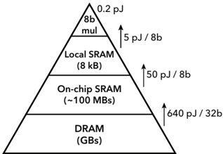
F igure 1 . 1 : Importance of data locality is shown in the memory hierarchy as the computation ( 8 b multiplication) costs only the fraction of the energy of memory access, in 45 nm CMOS [ 11 ].
<details>
<summary>Image 1 Details</summary>
### Visual Description
\n
## Diagram: Memory Hierarchy Energy Consumption
### Overview
The image is a triangular diagram representing a memory hierarchy, illustrating the trade-off between memory size/distance from the processor and energy consumption per bit. The diagram shows four levels of memory: 8b multiplier, Local SRAM, On-chip SRAM, and DRAM, arranged from top to bottom, representing increasing size and distance from the processor. Energy consumption per bit increases as you move down the hierarchy.
### Components/Axes
The diagram consists of four horizontal layers, each representing a different memory type. Arrows indicate the energy consumption per bit for each level. The diagram does not have traditional axes, but the vertical position represents the distance from the processor (closer at the top, further at the bottom) and implicitly, the speed of access.
* **Top Layer:** 8b multiplier, labeled with "0.2 pJ"
* **Second Layer:** Local SRAM (8 kB), labeled with "5 pJ / 8b"
* **Third Layer:** On-chip SRAM (~100 MBs), labeled with "50 pJ / 8b"
* **Bottom Layer:** DRAM (GBs), labeled with "640 pJ / 32b"
### Detailed Analysis or Content Details
The diagram illustrates the energy cost associated with accessing different types of memory.
* **8b multiplier:** Consumes 0.2 picojoules (pJ).
* **Local SRAM (8 kB):** Consumes 5 pJ per 8 bits.
* **On-chip SRAM (~100 MBs):** Consumes 50 pJ per 8 bits.
* **DRAM (GBs):** Consumes 640 pJ per 32 bits.
The energy consumption increases significantly as you move down the memory hierarchy. The DRAM level has the highest energy consumption, while the 8b multiplier has the lowest. The units are not consistent across all levels (pJ vs. pJ/bit).
### Key Observations
* There is a clear trend of increasing energy consumption as memory size increases and distance from the processor grows.
* The energy consumption per bit is significantly higher for DRAM compared to the other memory levels.
* The diagram highlights the importance of using a memory hierarchy to optimize energy efficiency.
* The units are inconsistent, making direct comparison difficult. DRAM is measured in pJ/32b while the others are pJ/8b.
### Interpretation
This diagram demonstrates the fundamental principle behind memory hierarchies in computer architecture. Smaller, faster, and closer memory (like the 8b multiplier and Local SRAM) is more energy-efficient but also more expensive and limited in capacity. Larger, slower, and more distant memory (like DRAM) is cheaper and has higher capacity but consumes significantly more energy per access.
The diagram suggests that a well-designed memory hierarchy aims to keep frequently accessed data in the faster, more energy-efficient levels, minimizing the need to access the slower, more energy-intensive levels. The inconsistent units suggest a focus on illustrating the *relative* energy costs rather than precise absolute values. The use of approximate values (~100 MBs) for On-chip SRAM further reinforces this point.
The diagram is a simplified representation, but it effectively conveys the trade-offs involved in memory system design. It implies that optimizing energy consumption requires careful consideration of memory size, speed, and distance from the processor.
</details>
(i.e., DRAM → on-chip SRAM → local SRAM), incurring roughly an order of magnitude more energy and latency penalty. Even in the ideal case of local SRAM, the cost of memory access exceeds that of computation by an order of magnitude. In-memory computing offers a compelling
3 On edge Tensor Processing Unit (TPU) for instance, memory access can consume over 90% of the total energy, throttle throughput to below 10% peak capacity, and in general dominate the majority of chip area [ 12 ].
alternative to data movement by processing data where it is stored, and one of the most promising technologies for in-memory computing is memristors.
Memristors are two-terminal analog resistive memory devices capable of both computation and memory [ 13 ]. They have a unique ability to encode and store information in their electrical conductance, which can be altered based on the history of applied electrical pulses [ 14 ]. Because a single memristor's conductance can transition between multiple levels between Low Conductive State (LCS) and High Conductance State (HCS), it can store more than one bit of information (typically between to 3 and 5 bits) improving the memory density. 4 Various memristor types exist, each with distinct operating principles and advantages. For example, PCM relies on the contrasting electrical resistance of amorphous and crystalline phases in chalcogenide materials [ 16 , 17 ], RRAM operates by altering the resistance of dialectric material through the drift of oxygen vacancies or the formation of conductive filaments [ 18 ], and Ferroelectric Random Access Memory (FeRAM) uses the polarization of ferroelectric materials to store and change information [ 19 ]. Although the electrical interface to these types does not differ significantly (applying electrical pulses to read or program the conductance), these underlying mechanisms determine the device's switching speed, footprint, stochasticity, endurance, and energy efficiency.
When implementing functions with memristor forms, it is helpful to categorize by volatility. Non-volatile memristors retain conductance after programming, ideal for weight storage in neural networks. This property extends to in-memory computing to perform dot-product operations [ 20 -22 ]. When an array of N memristive devices store vector elements Gi in their conductance states, applying voltages Vi to the devices and measuring the resulting currents I i , the dot product ∑ N i = 1 GiVi can be computed with O ( 1 ) complexity by Ohm's Law and Kirchoff's current law. This principle extends to matrix-vector multiplication, enabling neural network inference directly through the analog substrate's physics. In-memory neural inference has been demonstrated in large prototypes like the PCM-based HERMES chip [ 23 ] and RRAM-based NeuRRAM chip [ 18 ].
Volatile memristors, however, provide functionality beyond mere storage, and are often less explored. Their conductance decay within 10 ms to 100 ms allows for continuous-time, stochastic accumulate-and-decay functions, approximating low-pass filtering, signal averaging, or time tracking. In neural computations, volatile memristors have been used to implement short-term synaptic [ 24 , 25 ] and neuronal dynamics [ 26 , 27 ].
why spikes ? In this thesis, I focus on SNNs, where neural activations are represented as discrete pulses called spikes. This choice is primarily motivated by hardware considerations. Spikes enable extreme spatiotemporal sparsity, aligning well with asynchronous computation where energy consumption directly correlates with spiking events that trigger localized circuits [ 28 ]. Mixed-signal spiking neuron circuits inherently act as sigma-delta Analog-to-Digital Converters (ADCs), converting analog neural computation into digital spikes [ 29 ] for noise-robust transmission over long distances without signal degradation [ 30 ]. Additionally, spiking neurons seamlessly interface with reading and programming of memristive devices and also with event-based sensors [ 31 , 32 ] through Address-Event Representation (AER) [ 33 ] protocol. Spiking communication has even been proposed to mitigate severe heating issues in 3 D fabrication using n-ary coding schemes [ 34 ].
From a computational perspective, a common argument for spikes is efficient information encoding through precisely utilizing the temporal dimension (e.g., time-to-first-spike [ 35 ], phasecoding [ 36 ], or inter-spike-interval [ 37 ]). Furthermore, the spiking framework allows to formulate hypotheses about biophysical spike-based learning mechanisms in the brain [ 38 -40 ] and explore the computational capabilities of spiking neural networks [ 41 ], as demonstrated in our recent work. While a comprehensive exploration of the advantages of spikes is beyond this thesis's scope, the primary focus here is their potential for energy-efficient communication on analog substrates, as their unique computational benefits remain to be conclusively demonstrated.
4 These attributes are interestingly similar to biological synapses, where the synaptic efficacy is modulated by the history of pre- and post-synaptic activity, and is suggested to take 26 distinguishable strengths (correlated with spine head volume) [ 15 ].
## State of the Art
Despite their potential, memristors are not without their challenges for neural computing. In this section, I will outline some of these challanges in inference, learning and routing, and state-of-the-art attempts to address them.
Limited bit precision. Programming nanoscale memristive devices, modifies their atomic arrangement, inherently stochastic, non-linear and of limited granularity [ 42 -45 ]. This analog non-idealities are known to cause significant performance drops in training networks compared to software simulations [ 46 ]. Controlled experiments by Sidler et al. [ 22 ] have demonstrated that the poor training performance is primarily due to insufficient number of pulses switching the device between High Resistive State (HRS) and Low Resistive State (LRS).
Following this, various attempts have been made to improve the bit precision of memristive devices. Optimizing RRAM materials has increased the number of bits per device, but often at the cost of lower ON/OFF ratios (i.e., the ratio of the LRS and HRS), making it harder to distinguish states with small footprint circuits [ 47 -50 ]. Furthermore, architectural optimizations have been explored, including using multiple binary devices per synapse [ 51 ], assigning a number system to multiple devices [ 52 ], leveraging stochastic switching [ 53 , 54 ], and complementing binary memristive devices with capacitors [ 55 ]. However, these methods still require complex and large synaptic architectures, limiting scalability.
In Chapter 2 , we propose a novel approach to program intrinsically 1 -bit RRAM devices to increase their effective bit resolution by precise control of the filament formation.
The credit assignment problem. Learning in any systems is fundamentally about adjusting its parameters to improve its performance. In neural networks, learning involves adjusting weights, represented by the vector W , to optimize the performance, measured by an objective function, F ( W ) . The credit assignment problem refers to the challenge of determining the precise weight adjustments needed for improvement, especially in deep networks where the relationship between individual neurons and overall performance is less clear [ 56 ].
Traditionally, Hebbian mechanisms [ 57 ] leveraging the timing of pre- and post-synaptic spikes, have been the go-to solution for on-chip learning in the neuromorphic field. This is because Hebbian rules explain a numerous neuroscientific observations [ 58 , 59 ], posses interesting variance maximization properties [ 60 ] but more practically, utilize local signals to the synapse in a simple way, making them easily adaptable to silicon circuits [ 61 -64 ]. However, Hebbian rules alone had limited success while scaling to large networks, and require heavily crafted architectural biases to achieve hiererchical, disentangled representations. 5
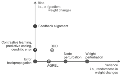
Backpropagation [ 68 ], on the other hand, remains the state-of-the-art algorithm for training modern ANNs, and is one of the pillars of the deep learning revolution. To give an intuition why it works, following the insight from Richards et al. [ 7 ], let's consider weight changes, ∆ W , to be small and objective function to be maximized, F , to be locally smooth, then resulting ∆ F can be approximated as ∆ F ≈ ∆ W T · ∇ WF ( W ) , where ∇ WF ( W ) is the gradient of the objective function with respect to the weights. This means that to guarantee improving learning performance ( ∆ F ≥ 0), a principled approach to weight adjustment is to take a small step in the direction of the steepest performance improvement, guided by the gradient ( ∆ F ≈ η ∇ WF ( W ) T · ∇ WF ( W ) ≥ 0). Backpropagation explicitly calculating gradients, while powerful, is unsuitable for online learning on analog substrates due to its need for symmetric feedback weights and distinct forward/backward phases [ 56 ]. And for temporal credit assignment, BPTT unrolls the network in reverse time to backpropagate the error gradients, resulting in memory complexity scaling with O ( kT ) , where k is the number of time steps and T is the number of neurons. This temporal nonlocality, necessitates the usage of memory hierarchy to save silicon space, resulting in sacrificing energy efficiency and latency. For this reason, various alternatives have been proposed to estimate gradients while offering better locality, such as feedback alignment [ 69 ], Q-AGREL [ 70 ], difference
5 While this is true, it is possible that end-to-end credit assignment might not be needed [ 65 ]. Recent works successfully replacing global backpropagation with truncated layer-wise backpropagation supports this view [ 66 , 67 ]. Nevertheless, designing the right architecture and local loss functions to guide the truncated credit assignment is still an open question.
target propagation [ 71 ], predictive coding [ 72 ] and weight perturbation-based methods [ 73 ]. These methods exhibit varying degrees of variance (resulting in slower convergence) and bias (leading to poor generalization [ 74 ]) in their estimations [ 7 ].
However, as long as variance and bias are within reasonable bounds, the learning rule can still be effective, potentially offering a favorable sweet spot between locality and performance. The challenge of local and effective spatio-temporal credit assignment is still a critical frontier in neural processing in analog substrates, demanding new and creative approaches.
In Chapter 3 , we address this challenge for the first time, designing material and circuits evolved around gradient calculations, and implementing e-prop [ 75 ] local learning rule for Recurrent Spiking Neural Networks (RSNNs) on a memristive chip.
## Programming memristors with non-idealities
for online learning. On-chip learning requires the ability to program the network weights in accordance with the demands of the learning rule. While digital systems often rely on quantization to optimize memory access [ 76 ] and associated mitigation techniques such as stochastic rounding [ 77 ], gradient scaling [ 78 ], quantization range learning [ 79 ] and optimizing the weight representation [ 80 ], analog memristive systems present unique challenges due to nonidealities such as conductance-dependent, non-linear, stochastic, and time-varying programming responses [ 81 ]. Then, it is crucial to identify which digital methods can be effectively transferred to analog systems while promising small footprint and energy overhead.
In Section 3 . 1 and 3 . 2 , we analyze several practical weight update schemes implementing an online learning rule for mixed-signal systems on a custom simulator, and later validate on a real neuromorphic chip.
Scalable synaptic eligibility traces for local learning. Many high-performing local rules rely on eligibility traces [ 39 , 82 -86 ], slow synaptic memory mechanisms that carry information forward in time. These traces bridge the temporal gap between synaptic activity occuring on millisecond timescale with network errors arising seconds later, helping to solve the distal reward problem [ 87 , 88 ]. While several neuromorphic platforms [ 89 -91 ] have incorporated synaptic eligibility traces for learning, this mechanism is one of the most costly building blocks in neural computation, due to quadratic scaling of the number of synapses. Digital implementations suffer from the memory-intensive nature of numerical trace calculations, leading to a von Neumann bottleneck [ 92 , 93 ]. Even in mixed-signal designs, the slow dynamics of eligibility traces require large capacitors leading to sacrifice of the scalability [ 94 ].
In Section 3 . 3 , we propose a novel and scalable implementation of synaptic eligibility traces using volatile memristors.
Unifiying volatile and non-volatile materials. Different neural building blocks require different volatility, bit precision, and endurance characteristics from the memristive devices, which are then tailored to meet these demands. For example, ANN inference workloads require linear non-volatile conductance response over a wide dynamic range for optimal weight update and minimum noise for gradient calculation [ 21 , 22 , 95 ]. Whereas SNNs often demand richer and multiple synaptic dynamics simultaneously e.g., short term conductance decay (to implement Short-Term Plasticity (STP) and eligibility traces [ 82 ]), non-volatile device states (to represent synaptic efficacy) and a probabilistic nature (to mimic synaptic vesicle releases [ 24 ]). However, optimizing different active memristive material for each of these features limits their suitability to a wide range of computational frameworks and ultimately increases the system complexity for most demanding applications. Moreover, these diverse specifications cannot always be implemented by combining
F igure 1 . 2 : Bias and variance in learning rules which estimate the gradients, even if they are not explicitly compute gradients. Figure taken from [ 7 ].
<details>
<summary>Image 2 Details</summary>
### Visual Description
\n
## Scatter Plot: Learning Algorithms and Their Characteristics
### Overview
The image presents a scatter plot illustrating the relationship between "Bias" (vertical axis) and "Variance" (horizontal axis) for various learning algorithms. Each algorithm is represented by a point on the plot, and question marks indicate uncertainty or areas requiring further investigation.
### Components/Axes
* **X-axis:** Labeled "Variance", with the clarifying text "i.e., randomness in weight changes". The scale is not explicitly marked, but appears to range from low variance on the left to high variance on the right.
* **Y-axis:** Labeled "Bias", with the clarifying text "i.e., ∇ (gradient, weight change)". The scale is not explicitly marked, but appears to range from low bias at the bottom to high bias at the top.
* **Data Points/Algorithms:**
* Feedback alignment
* Contrastive learning, predictive coding, dendritic error
* RDD (with a question mark)
* AGREL (with a question mark)
* Node perturbation
* Weight perturbation
* Error backpropagation
* **Question Marks:** Placed near the data points for "RDD" and "AGREL", and also near "Contrastive learning, predictive coding, dendritic error", indicating uncertainty in their precise positioning or characteristics.
### Detailed Analysis
The plot shows a general trend of increasing variance as bias decreases.
* **Feedback alignment:** Located in the top-left quadrant, indicating high bias and low variance. Approximate coordinates: (1, 9).
* **Contrastive learning, predictive coding, dendritic error:** Located in the upper-middle quadrant, indicating high bias and moderate variance. Approximate coordinates: (3, 7).
* **Error backpropagation:** Located in the lower-middle quadrant, indicating low bias and moderate variance. Approximate coordinates: (3, 2).
* **AGREL:** Located near the x-axis, indicating low bias and low variance. Approximate coordinates: (4, 1).
* **RDD:** Located between AGREL and Contrastive learning, predictive coding, dendritic error, indicating low bias and moderate variance. Approximate coordinates: (5, 4).
* **Node perturbation:** Located on the x-axis, indicating low bias and high variance. Approximate coordinates: (6, 1).
* **Weight perturbation:** Located on the x-axis, indicating low bias and very high variance. Approximate coordinates: (7, 1).
The positioning of the algorithms suggests a trade-off between bias and variance. Algorithms with high bias tend to have low variance, and vice versa.
### Key Observations
* The algorithms cluster along a diagonal, suggesting a negative correlation between bias and variance.
* The question marks highlight areas where the positioning of the algorithms is uncertain or requires further investigation.
* Error backpropagation, AGREL, Node perturbation, and Weight perturbation are positioned relatively close to the x-axis, indicating low bias.
* Feedback alignment and Contrastive learning, predictive coding, dendritic error are positioned relatively high on the y-axis, indicating high bias.
### Interpretation
This plot illustrates a fundamental concept in machine learning: the bias-variance trade-off. Algorithms with high bias make strong assumptions about the data, leading to low variance but potentially high errors if the assumptions are incorrect. Algorithms with low bias make fewer assumptions, leading to high variance and potentially overfitting the data.
The positioning of the algorithms on the plot suggests their relative strengths and weaknesses. For example, Feedback alignment is a high-bias, low-variance algorithm, which might be suitable for simple problems where strong assumptions are valid. Weight perturbation is a low-bias, high-variance algorithm, which might be suitable for complex problems where flexibility is important.
The question marks indicate that the positioning of RDD, AGREL, and Contrastive learning, predictive coding, dendritic error is uncertain, suggesting that further research is needed to understand their characteristics. The plot provides a useful visual representation of the trade-off between bias and variance, and can help guide the selection of appropriate learning algorithms for different problems.
</details>
different types of memristors on a monolithic circuit e.g., volatile and non-volatile, binary and analog, due to the incompatibility of the fabrication processes. Although some prototype materials have been proposed to exhibit dual-functional memory [ 96 , 97 ], the dominance of one of the mechanisms often results in poor switching performance. Therefore, the lack of universal memristors capable of realizing diverse computational primitives has been a challenge.
In Chapter 4 , we present our discovery of a novel memristor type that can be used for both volatile and non-volatile operations based on a simple programming scheme, while achieving a world-record in endurance.
Routing of multi-crossbar arrays for scaling. Scaling neural networks, by increasing layer width or depth, has proven to be a powerful technique for improving performance [ 98 ]. However, scaling memristive crossbar array dimensions is hindered by analog non-idealities such as current sneak-paths, parasitic resistance, capacitance of metal lines, and yield limitations [ 99 -101 ]. For this reason, large-scale systems need to adapt multiple crossbars of managable dimensions [ 102 ], but this introduces the overhead of routing activities, especially with long wires along the source, router and destination. To reduce wiring length, three-dimensional ( 3 D) technology to vertically stack logic, crossbar arrays, and routers has been proposed [ 34 , 102 ], but the fabrication complexity and cost of 3 D integration are currently prohibitive. Today's most advanced multi-crossbar neuromorphic chips, e.g., HERMES [ 23 ] and NeuRRAM [ 18 ], still rely on off-chip communication for routing, strongly diminishing communication energy efficiency. This necessitates the development of efficient on-chip routing mechanisms to achieve energy-efficient communication. When the routing is optimized for communicating events through the on-chip AER protocol, the designer faces a trade-off between source-based and destination-based routing. Source-based routing offers the flexibility of per-neuron Content Addressable Memory (CAM) memory as used by DYNAP-SE [ 103 ], but this comes at the cost of increased chip area and slower memory access. Destination-based routing, while more area-efficient, sacrifices some degree of network configurability.
In Chapter 5 , we propose and fabricate a novel memristive in-memory routing core that can be reconfigured to route signals between crossbars, enabling dense local, sparse global connectivity with orders of magnitude more routing efficiency compared to other SNN hardware platforms.
## Thesis Overview
This thesis explores the path towards intelligent and low-power analog computing substrates, embracing the Bitter Lesson [ 104 ] and addressing some of the challenges in learning and scale. It consists of six selected publications, which I have coauthored with amazing electrical engineers, computer scientists, material designers and neuroscientists. My individual contributions to the work presented in each chapter are clarified and outlined in Appendix 4 .
In the first part, we focus on developing mixed-signal learning circuits targeting memristive weights in single-layer feedforward SNN architectures. We address the limited resolution and device-to-device and cycle-to-cycle variability of binary RRAM weights, aiming to enable on-chip learning. Building upon the observation of Ielmini [ 105 ] that filament size in RRAM can be precisely controlled by compliance current, we introduce a programming circuitry that modulates synaptic weights based on the estimated gradients using a modified Delta Rule [ 106 ]. This approach achieves multi-level weight resolution within the conductance of intrinsically binary switching RRAM devices. We model variability of device responses to our new compliance current programming scheme, I CC to G LRS, from experimental measurements on a 4 kb HfO 2 -based RRAM array, and adjust our implementation accordingly. We validate our approach and circuits through simulations for standard Complementary Metal-Oxide-Semiconductor (CMOS) 180 nm processes and system simulations on the MNIST dataset. This codesign of algorithm, material, and circuit properties establishes a significant building block for single-layer on-chip learning with memristive devices. Furthermore, in Chapter 4 , we demonstrate that our programming
scheme can also be applied, with even more linear response, to novel perovskite memristors.
In Chapter 3 , we extend our focus to more challenging task of training RSNNs on-chip, addressing the complexities of online temporal credit assignment with memristive devices for in-memory computing. Our work encompasses three complementary efforts: 1 ) given a recent local learning rule development for RSNNs [ 75 ], investigating how to reliably program analog devices based on a realistic PCM model on simulations, 2 ) validating these results on a PCM-based neuromorphic chip, and 3 ) proposing a scalable implementation of synaptic eligibility traces, a crucial component of many local learning rules, using volatile memristors.
To achieve this, we start with developing a PyTorch [ 107 ]-based simulation framework based on a comprehensive statistical model of a PCM crossbar array, capturing the major device nonidealities: programming noise, read noise, and temporal drift [ 81 ]. Our selected learning rule, e-prop, estimates the gradient with nice locality constraints, but it is not known how to reflect the gradient signal reliably while programming memristors with non-idealities. This framework enables benchmarking four commonly practiced memristor-aware weight update mechanisms (Sign-Gradient Descent [ 108 ], stochastic updates [ 81 ], multi-memristor updates [ 109 ] and mixedprecision [ 110 ]), to reliably program memristors conductances based on estimated gradients on generic regression tasks. We show that mixed-precision update scheme is superior by accumulating gradients on a high-precision memory (similar to quantization-aware-training methods [ 111 ]), allowing for a lower learning rate and improved alignment of weight update magnitudes with the PCM's minimum programmable conductance change. It also reduces the total number of write pulses by 2 -3 orders of magnitude, reducing energy spent on costly memristive programming and mitigating potential endurance issues. Furthermore, we verified previous digital implementations [ 77 ] of the stochastic update working well down to 8 -bit precision digital simulations.
Following simulations, the next step is to validate it on a physical neuromorphic chip. We implemented the e-prop learning rule on the HERMES chip [ 23 ], fabricated in 14 nm CMOS, with four 256 x 256 PCM crossbar arrays in a differential parallel setup. We programmed all weights of a RSNN onto physical PCM devices across HERMES cores for in-memory inference. On-chip training was controlled by a digital coprocessor implementing a mixed-precision algorithm to accumulate gradients on a high-precision memory unit. Our mixed-precision training on HERMES achieved performance competitive with conventional software simulations, maintained a regularized firing rate, and significantly reduced the number of PCM programming pulses, enhancing energy efficiency. Our results demonstrates the first successful implementation of a gradient-based, powerful online learning rule for RSNNs on an analog substrate. While the mixed-precision technique requires an additional high-precision memory unit, we demonstrate that inference can be in-memory, and off-chip guided learning can be activated as needed with minimal analog device programming.
Local learning rules, including e-prop, often require synaptic eligibility traces [ 39 , 82 -86 ], posing a scaling challenge for analog hardware due to their O ( N 2 ) area scaling, where N is the number of neurons. This challenge is exacerbated by increased time-constant requirements, as larger capacitors are needed for implementation. To address this, we introduce PCM-trace, a novel small-footprint circuitry leveraging the inherent conductance drift of PCM to emulate eligibility traces for local learning rules. We exploit the material bug - the structural relaxation and temporal conductance drift in PCM's amorphous regime [ 112 ], described by R ( t ) = R ( t 0 )( t t 0 ) ν - turning it into a feature. Our optimized material choice allows gradual SET pulses to accumulate the trace, while conductance naturally decays over seconds. We also introduce a multi-PCM-trace configuration, distributing synaptic traces across multiple PCM devices to significantly improve dynamic range. Experimental results on 130 nm CMOS technology confirm that PCM-trace can maintain eligibility traces for over 10 seconds while offering more than 11 x area savings compared to conventional capacitor-based trace implementations [ 94 ].
In Chapter 4 , we introduce a state-of-the-art memristive material based on halide perovskite nanocrystals that can be dynamically reconfigured to exhibit volatile or non-volatile behavior. This is motivated by the fact that many in-memory neural computing systems demand devices with specific switching characteristics, and existing memristive devices cannot be reconfigured to meet these diverse volatile and non-volatile switching requirements. To achieve this, we develop a cesium lead bromide nanocrystals capped with organic ligands as the active switching matrix and silver as the active electrode. This design leverages the low activation energy of ion migration in halide perovskites to achieve both diffusive (volatile) and drift (non-volatile) switching. By actively controlling the compliance current ( Icc ) following our prior work at Chapter 2 , the magnitude of ion flux is adjusted, enabling on-demand switching between the two modes. This control mechanism allows for the selection of diffusive dynamics with low Icc (1 µ A) for volatile behavior and drift kinetics with higher Icc ( 1 mA) for non-volatile memory operation. Moreover, our measurements demonstrated that memristors using perovskite nanocrystals capped with OGB, achieve a record endurance in both volatile and non-volatile modes. We attribute this superior performance to the larger OGB ligands, which better insulate the nanocrystals and regulate the electrochemical reactions responsible for switching behavior.
In Chapter 5 , we switch gears and focus on the scalability of memristive architectures in neuromorphic systems, a challenge hindered by analog non-idealities of crossbar arrays. We introduce Mosaic, a novel memristive systolic array architecture consisting of interconnected Neuron Tiles and Routing Tiles, both implemented with RRAM integrated 130 nm CMOS technology.
Each Neuron Tile, per usual, is a crossbar array of memristors storing network weights for a RSNN layer with Leaky Integrate-and-Fire (LIF) neurons. These neurons emit spikes based on integrated synaptic inputs, transmitting them to neighbouring tiles through Routing Tiles. The Routing Tiles, also based on memristor arrays, define the connectivity patterns between Neuron Tiles. The resulting structure then becomes a small-world graph with dense local and sparse long-range connections, similar to the connectivity found in biological brains 6 .
Our in-memory routing approach necessitates careful optimization of connectivity during offline training to prune RSNNs into a Mosaic-compatible, small-world graph. We introduce a novel hardware layout-aware training method that considers the physical layout of the chip and optimizes neural network weights using either gradient-based or evolutionary algorithms [ 113 ].
In-memory routing and optimization for sparse long-range and locally dense communication in Mosaic result in significant energy efficiency in spike routing, surpassing other SNN hardware platforms by at least one order of magnitude, as demonstrated by hardware measurements and system-level simulations. Notably, due to its layout-aware structured sparsity, Mosaic achieves competitive accuracy in edge computing tasks like biosignal anomaly detection, keyword spotting, and motor control.
6 It may not be a coincidence that some of the solutions proposed in this thesis can also be found in the biological brain, whispering of a deep connection between highly optimized silicon substrates and the evolved neural tissue.
<details>
<summary>Image 3 Details</summary>

### Visual Description
Icon/Small Image (61x83)
</details>
## ENHANCING BIT PRECISION OF BINARY MEMRISTORS FOR ROBUST ON-CHIP LEARNING
This chapter's content was published in IEEE International Symposium on Circuits and Systems (ISCAS). The original publication is authored by Melika Payvand, Yigit Demirag, Thomas Dalgaty, Elisa Vianello, Giacomo Indiveri.
Analog neuromorphic circuits with memristive synapses offer the potential for power-efficient neural network inference, but limited bit precision of memristors poses challenges for gradientbased training. In this chapter, we introduce a programming technique of the weights to enhance the effective bit precision of initially binary memristive devices, enabling more robust and performant on-chip training. To overcome the problems of variability and limited resolution of ReRAM memristive devices used to store synaptic weights, we propose to use only their HCS and control their desired conductance by modulating their programming compliance current, ICC . We introduce spike-based CMOS circuits for training the network weights; and demonstrate the relationship between the weight, the device conductance, and the ICC used to set the weight, supported with experimental measurements from a 4 kb array of HfO 2 -based devices. To validate the approach and the circuits presented, we present circuit simulation results for a standard CMOS 180 nm process and system-level simulations for classifying hand-written digits from the MNIST dataset.
## 2 . 1 introduction
The neural networks deployed on the resource-constrained devices can benefit greatly from online training to adapt to shifting data distributions, sensory noise, device degradation, or new tasks that are not seen in the pretraining. While CMOS architectures with integrated memristive devices offer ultra-low power inference, their use for online learning has been limited [ 114 , 115 ].
In this chapter, we propose novel learning circuits for SNN architectures implemented by 1 T 1 R arrays. These circuits enable analog weight updates on binary ReRAM devices by controlling their SET operation ICC . In addition to increasing the bit precision of network weights, the proposed strategy allows compact, fast, and scalable event-based learning scheme compatible with the AER interface [ 116 ].
Previously significant efforts have aimed to increase the bit precision of memristive devices for online learning through material and architectural optimizations.
material optimization Several groups reported TiO 2 -based [ 47 -49 ] and HfO 2 -based [ 50 ] ReRAM devices with up to 8 bits of precision. However, in all these works, the analog behavior is traded off with the lower available ON/OFF ratio. While the analog behavior is an important concern for training neural networks, cycle-to-cycle and device-to-device variability harms the effective number of bits further when ON/OFF ratio is small. Also, tuning the precise memory state is not always easily achievable in a real-time manner, requiring recursively tuning with an active feedback scheme [ 50 , 117 ]. Furthermore, some efforts have been focused on carefully designing a barrier level using exhaustive experimental search over a range of materials [ 47 , 48 ] which makes it difficult to fabricate.
architecture optimization Increasing the effective bit resolution has also been demonstrated with architectural advancements. Strategies such as using multiple binary switches to emulate n-bit synapses [ 51 ] or exploiting stochastic switching properties for analog-like adaptation [ 53 , 54 ] have been explored. Alternatively, IBM's approach of using a capacitor alongside two PCM devices to act as an analog volatile memory, increases combined precision but incurs significant area overhead [ 55 ]. Recently, a mixed-precision approach has been employed to train
the networks using a digital coprocessor for weight update accumulation [ 118 ], but requires digital buffering of weights, gradients and suffers of domain-conversion costs.
Thus, neither device nor architecture optimizations have fully resolved the challenges of low bit precision in memristors for online learning. Prior work by Ielmini [ 105 ] observed that the electrical resistance of memristors after a SET operation follows a linear relationship with ICC in a log-log scale, by control over the size of the filament. This critical observation underpins our approach, where we exploit this relationship to directly control device conductance.
To minimize the effect of variability, we adopt an algorithm-device codesign approach. We restrict devices to stay only in their HCS and modulate their conductance by adjusting the programming ICC . Specifically, we derive a technologically feasible online learning algorithm based on the Delta rule [ 106 ], mapping weight updates onto the ICC used for setting the device. This co-design offers several advantages: (i) relaxed fabrication constraints compared to multi-bit devices, and (ii) increased state stability due to the use of only two levels per device.
## 2 . 2 reram device modeling
To find the average relationship between the mean of the cycle-to-cycle distribution of the HCS and the SET programming ICC , we performed measurements on a 16 × 256 ( 4 kb) array of HfO 2 -based ReRAM devices integrated onto a 130 nm CMOS process between metal layers 4 and 5 [ 119 ]. Each device is connected in series to the drain of an n-type selector transistor which allows the SET programming ICC to be controlled based on the voltage applied to its gate. The 1 T 1 R structure allows a single device to be selected for reading or programming by applying appropriate voltages to a pair of Source/Bit Lines (SL/BL) and a single Word Line (WL).
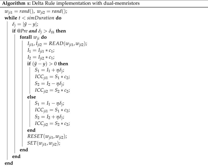
All 4 kb devices were initially formed in a raster scan fashion by applying a large voltage ( 4 V typical) between the SL and BL to induce a soft breakdown in the oxide layer and introduce conductive oxygen vacancies. After forming, each device was subject to sets of 100 RESET/SET cycles over a range of SET ICC s between 10 µ A and 400 µ A, where the resistance of each device was recorded after each SET operation. The mean of all devices' median resistances over the 100 cycles, at a single ICC , gives the average relationship between HCS median and SET ICC as in Fig. 2 . 1 . The relationship is seen to follow a line in the log-log plot (power law) and over this ICC range, it allows precise control of the conductance median of the cycle-to-cycle distribution between 50 k Ω and 2 k Ω .
## 2 . 3 bit -precision enhancing weight update rule
The learning algorithm is based on the Delta rule, the simplest form of the gradient descent for single-layer networks. In our implementation, the objective function is defined as the difference between the desired target output signal y and the network prediction signal ˆ y , for a given set of input patterns signals x , weighted by the synaptic weight parameters w . Then the Delta rule can be used to calculate the change of the weights connecting a neuron i in the input layer and a neuron j at the output layer as follows:
$$\Delta w _ { j i } = \eta ( y _ { j } - \hat { y } _ { j } ) x _ { i } = \eta \delta _ { j } \, x _ { i } , & & ( 2 . 1 )$$
F igure 2 . 1 : Mean and standard deviation of the device conductance as a function of the ICC s. The inset shows the samples from the fitted mean and standard deviation used for the simulations.
<details>
<summary>Image 4 Details</summary>
### Visual Description
\n
## Chart: Conductance vs. Current
### Overview
The image presents a graph illustrating the relationship between conductance (G<sub>LRS</sub>) and current (I<sub>CC</sub>). The main plot shows a logarithmic scale for both axes, displaying a clear upward trend. An inset plot provides a more detailed view of the data at higher current values, also on a logarithmic scale. Error bars are present on the main plot, indicating the uncertainty in the conductance measurements.
### Components/Axes
* **X-axis:** I<sub>CC</sub> (A) - Current, labeled in Amperes. The scale is logarithmic, ranging from approximately 10<sup>-5</sup> A to 10<sup>-4</sup> A.
* **Y-axis:** G<sub>LRS</sub> (S) - Conductance, labeled in Siemens. The scale is logarithmic, ranging from approximately 10<sup>-5</sup> S to 10<sup>-4</sup> S.
* **Data Series:** A single blue line with circular data points represents the conductance as a function of current.
* **Error Bars:** Vertical error bars are associated with each data point on the main plot, indicating the uncertainty in the conductance measurements.
* **Inset Plot:** A smaller plot in the top-right corner, also showing G<sub>LRS</sub> (S) on the Y-axis and I<sub>CC</sub> (A) on the X-axis, but with a different scale. The inset plot appears to show a scatter plot of many data points.
### Detailed Analysis
The main plot shows a strong positive correlation between I<sub>CC</sub> and G<sub>LRS</sub>. The line slopes sharply upwards initially, then gradually flattens out as I<sub>CC</sub> increases.
Here's an approximate extraction of data points from the main plot, noting the logarithmic scales and error bar uncertainties:
* I<sub>CC</sub> = 10<sup>-5</sup> A, G<sub>LRS</sub> ≈ 3 x 10<sup>-5</sup> S (with an error bar extending to approximately 5 x 10<sup>-5</sup> S)
* I<sub>CC</sub> = 3 x 10<sup>-5</sup> A, G<sub>LRS</sub> ≈ 1 x 10<sup>-4</sup> S (with an error bar extending to approximately 2 x 10<sup>-4</sup> S)
* I<sub>CC</sub> = 6 x 10<sup>-5</sup> A, G<sub>LRS</sub> ≈ 2 x 10<sup>-4</sup> S (with an error bar extending to approximately 3 x 10<sup>-4</sup> S)
* I<sub>CC</sub> = 1 x 10<sup>-4</sup> A, G<sub>LRS</sub> ≈ 3.5 x 10<sup>-4</sup> S (with an error bar extending to approximately 4.5 x 10<sup>-4</sup> S)
* I<sub>CC</sub> = 2 x 10<sup>-4</sup> A, G<sub>LRS</sub> ≈ 5 x 10<sup>-4</sup> S (with an error bar extending to approximately 6 x 10<sup>-4</sup> S)
* I<sub>CC</sub> = 3 x 10<sup>-4</sup> A, G<sub>LRS</sub> ≈ 6 x 10<sup>-4</sup> S (with an error bar extending to approximately 7 x 10<sup>-4</sup> S)
* I<sub>CC</sub> = 4 x 10<sup>-4</sup> A, G<sub>LRS</sub> ≈ 6.5 x 10<sup>-4</sup> S (with an error bar extending to approximately 7.5 x 10<sup>-4</sup> S)
The inset plot shows a dense scatter of points, also exhibiting a positive correlation, but with more scatter than the main plot. The data points in the inset appear to cluster around a similar trend as the main plot, but with a higher density of data.
### Key Observations
* The conductance increases significantly with increasing current, especially at lower current values.
* The rate of increase in conductance slows down at higher current values, suggesting a saturation effect.
* The error bars indicate a considerable degree of uncertainty in the conductance measurements, particularly at lower current values.
* The inset plot provides a more detailed view of the data, confirming the overall trend observed in the main plot.
### Interpretation
The data suggests a non-linear relationship between conductance and current. This could be indicative of a switching behavior in the material or device under investigation. The initial steep increase in conductance with current might represent a transition from a high-resistance state to a low-resistance state. The subsequent flattening of the curve suggests that the material reaches a saturation point where further increases in current do not significantly increase the conductance.
The error bars highlight the variability in the measurements, which could be due to factors such as noise, device-to-device variations, or measurement limitations. The inset plot provides a more granular view of the data, potentially revealing finer details about the conductance-current relationship. The consistent trend observed in both the main plot and the inset plot strengthens the conclusion that there is a clear correlation between conductance and current in this system. The logarithmic scales suggest that the relationship is exponential or power-law-like. This type of behavior is often observed in memristive devices or other systems exhibiting non-linear electrical characteristics.
</details>
<details>
<summary>Image 5 Details</summary>
### Visual Description
\n
## Algorithm: Delta Rule Implementation with Dual-Memristors
### Overview
The image presents a pseudocode algorithm titled "Delta Rule Implementation with Dual-Memristors". It outlines a learning rule, likely for a neural network, utilizing dual-memristor devices. The algorithm iteratively adjusts weights based on the difference between a target output and an actual output.
### Components/Axes
The content is structured as a pseudocode block with the following key elements:
* **Initialization:** `wji1 = rand(); wji2 = rand();` - Initializes weights `wji1` and `wji2` with random values.
* **Loop Condition:** `while t < simDuration do` - The algorithm iterates as long as the simulation time `t` is less than `simDuration`.
* **Error Calculation:** `δj = |ŷ - y|` - Calculates the error `δj` as the absolute difference between the target output `ŷ` and the actual output `y`.
* **Conditional Statement:** `if @Pre and δj > δth then` - Executes the following block only if the condition `@Pre` is true and the error `δj` is greater than a threshold `δth`.
* **Inner Loop:** `forall wji do` - Iterates through all weights `wji`.
* **Read Operation:** `Iji1, Iji2 = READ(wji1, wji2);` - Reads current values from memristors `wji1` and `wji2`, assigning them to `Iji1` and `Iji2`.
* **Intermediate Calculations:** `I1 = Iji1 * c1; I2 = Iji2 * c1;` - Calculates intermediate values `I1` and `I2` by multiplying the read currents with a constant `c1`.
* **Conditional Update (Positive Error):** `if (ŷ - y) > 0 then` - Executes the following block if the difference between the target and actual output is positive.
* `S1 = I1 + ηδj; ICCji1 = S1 * c2;` - Updates `S1` and calculates `ICCji1`.
* `S2 = I2 - ηδj; ICCji2 = S2 * c2;` - Updates `S2` and calculates `ICCji2`.
* **Conditional Update (Negative Error):** `else` - Executes the following block if the difference between the target and actual output is not positive (i.e., negative or zero).
* `S1 = I1 - ηδj; ICCji1 = S1 * c2;` - Updates `S1` and calculates `ICCji1`.
* `S2 = I2 + ηδj; ICCji2 = S2 * c2;` - Updates `S2` and calculates `ICCji2`.
* **Reset Operation:** `RESET(wji1, wji2);` - Resets the memristors `wji1` and `wji2`.
* **Set Operation:** `SET(wji1, wji2);` - Sets the memristors `wji1` and `wji2`.
* **End Statements:** `end`, `end` - Terminates the inner and outer loops.
### Detailed Analysis or Content Details
The algorithm describes a learning process where weights are adjusted based on the error signal. The use of `READ` and `RESET/SET` operations suggests the algorithm is designed for memristor-based hardware implementation. The constants `c1` and `c2` likely represent device characteristics. The parameter `η` (eta) appears to be a learning rate. The `@Pre` condition is not defined, suggesting it might be a hardware-specific pre-condition.
### Key Observations
The algorithm implements a delta rule, a classic supervised learning algorithm. The use of memristors introduces non-linearity and potentially energy efficiency. The conditional updates based on the sign of the error indicate a gradient-based learning approach. The `READ` operation suggests the memristor's state is read before weight updates.
### Interpretation
This algorithm demonstrates a potential implementation of a neural network learning rule using memristor devices. The algorithm leverages the unique properties of memristors – their ability to retain state and perform analog computation – to implement weight storage and updates. The `READ`, `RESET`, and `SET` operations are crucial for interacting with the memristor hardware. The algorithm's performance would depend on the specific characteristics of the memristors (represented by `c1` and `c2`) and the learning rate `η`. The `@Pre` condition suggests a hardware-level requirement for the learning process to proceed. The use of absolute value in the error calculation `δj = |ŷ - y|` suggests the algorithm is not sensitive to the sign of the error during the initial error calculation, but the sign is used to determine the direction of weight updates. This is a standard approach in delta rule implementations. The algorithm is a simplified model and may require further refinement for practical applications, such as handling multiple layers or more complex activation functions.
</details>
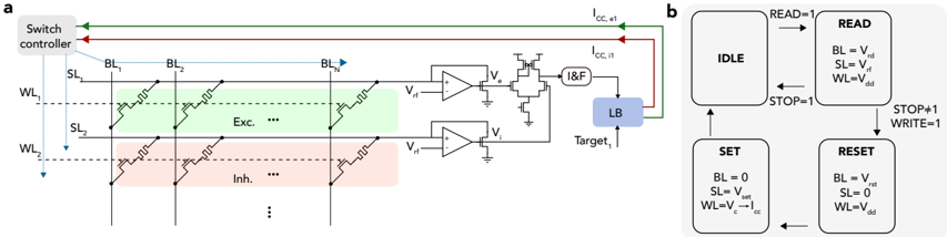
F igure 2 . 2 : Event-based neuromorphic architecture using online learning in a 1 T 1 R array (a), and the asynchronous state machine used as the switch controller applying the appropriate voltages on the BL, SL and WL of the array for online learning.
<details>
<summary>Image 6 Details</summary>
### Visual Description
\n
## Diagram: Memory Cell Circuit and State Diagram
### Overview
The image presents a schematic diagram of a memory cell circuit (labeled 'a') alongside a state diagram illustrating its operational modes (labeled 'b'). The circuit appears to be a non-volatile memory cell, likely a resistive RAM (ReRAM) or similar technology, with excitation (Exc.) and inhibition (Inh.) phases. The state diagram shows the transitions between IDLE, READ, SET, and RESET states.
### Components/Axes
**Part a (Circuit Diagram):**
* **Switch Controller:** Green arrow indicating control signals.
* **BL:** Bit Line (two instances, labeled BL and BL̅)
* **SL:** Select Line (two instances, labeled SL and SL̅)
* **WL:** Word Line (two instances, labeled WL and WL̅)
* **V<sub>T</sub>:** Threshold Voltage (two instances)
* **cc, v1:** Positive supply voltage.
* **cc, n:** Negative supply voltage.
* **LB:** Load Balance (blue oval)
* **Target:** Output signal.
* **&F:** AND/Flip-Flop gate.
* **Exc.:** Excitation region (highlighted in green).
* **Inh.:** Inhibition region (highlighted in red).
* **Dotted Lines:** Represent continuation of the memory array.
**Part b (State Diagram):**
* **IDLE:** Initial state.
* **READ:** State for reading the memory cell value.
* **SET:** State for setting the memory cell to a high resistance state.
* **RESET:** State for resetting the memory cell to a low resistance state.
* **READ = 1:** Transition from IDLE to READ.
* **STOP = 1:** Transition from IDLE to SET.
* **STOP + 1 WRITE = 1:** Transition from IDLE to RESET.
* **BL = V<sub>T</sub>, SL = V<sub>T</sub>, WL = V<sub>W</sub>:** Conditions for READ state.
* **BL = 0, SL = V<sub>T</sub>, WL = V<sub>SET</sub>:** Conditions for SET state.
* **BL = V<sub>T</sub>, SL = 0, WL = V<sub>RESET</sub>:** Conditions for RESET state.
### Detailed Analysis or Content Details
**Part a (Circuit Diagram):**
The circuit consists of two parallel memory cells, each with a bit line (BL/BL̅), select line (SL/SL̅), and word line (WL/WL̅). The excitation region (Exc.) shows a series of pulses applied to the word lines, while the inhibition region (Inh.) shows a similar pattern. The bit lines are connected to a differential amplifier and an AND/Flip-Flop gate. The Load Balance (LB) signal is connected to the output. The circuit utilizes complementary signals (BL/BL̅, SL/SL̅, WL/WL̅) for operation.
**Part b (State Diagram):**
The state diagram shows a four-state machine.
* From IDLE, the system transitions to READ upon receiving a READ signal (READ = 1).
* From IDLE, the system transitions to SET upon receiving a STOP signal (STOP = 1).
* From IDLE, the system transitions to RESET upon receiving a STOP + 1 WRITE signal.
* The READ state is defined by BL = V<sub>T</sub>, SL = V<sub>T</sub>, and WL = V<sub>W</sub>.
* The SET state is defined by BL = 0, SL = V<sub>T</sub>, and WL = V<sub>SET</sub>.
* The RESET state is defined by BL = V<sub>T</sub>, SL = 0, and WL = V<sub>RESET</sub>.
### Key Observations
* The circuit utilizes a differential sensing scheme with the differential amplifier.
* The excitation and inhibition regions suggest a pulse-based operation for programming the memory cell.
* The state diagram clearly defines the conditions for each operation (READ, SET, RESET).
* The use of complementary signals (BL/BL̅, SL/SL̅, WL/WL̅) indicates a balanced circuit design.
* The Load Balance (LB) signal suggests a mechanism for stabilizing the memory cell operation.
### Interpretation
The diagram illustrates a memory cell architecture that leverages resistive switching behavior. The excitation and inhibition phases likely control the resistance state of the memory cell, allowing it to store information. The state diagram provides a clear understanding of the control signals and conditions required for each operation. The differential sensing scheme enhances the reliability of the read operation. The Load Balance signal is likely used to compensate for process variations and improve the overall performance of the memory cell. The circuit appears to be designed for non-volatile memory applications, where data retention is crucial. The use of pulses for excitation and inhibition suggests a potential for fine-grained control over the memory cell's resistance state, enabling multi-level cell (MLC) operation. The diagram suggests a robust and efficient memory cell design with a clear operational flow.
</details>
where δ j is the error, and η is the learning rate. To implement this using memristive synaptic architecture, we represent each synaptic weight w , by the combined conductance of two memristors, wji 1 and wji 2 , arranged in a push-pull differential configuration. This scheme extends the effective dynamic range of a single synapse to capture the negative values.
During the network operation, the target and the prediction signals are compared continuously to generate the error signal. With the arrival of a pre-synaptic event, if the error signal is larger than a small error threshold, the weight update process is initiated. The small error threshold that creates the "stop-learning" regime has been proposed to help the convergence of the neural networks with stochastic weight updates [ 120 ].
The implementation of the synaptic plasticity consists of three phases (Alg. 1 ). First, a READ operation is performed on every excitatory and inhibitory memristor to determine their conductance. Then the resulting current values ( I ji 1 and I ji 2 ) are scaled to the level of the error signal. Second, the current value proportional to the amount of the weight change ηδ j xi is summed up with the scaled READ current to represent the desired conductance strength to be programmed. Finally, these currents are further scaled to a valid ICC range using linear scaling constants c 1 and c 2. To provide a larger dynamic range per synapse, the conductance of both memristors are updated with a push-pull mechanism considering the sign of the error (i.e. if the conductance of one memristor increased, the conductance of the complementary memristor is decreased, and vice-versa).
## 2 . 4 learning circuits and architecture
F igure 2 . 3 : Learning circuits generating the ICC for updating the devices based on the distance between the neuron and its target frequency. Highlighted in red is the Gm-C filters, low pass filtering the neuron and target spikes giving rise to VN and VT . In green and orange, the error between the two is calculated generating positive ( I ErrP ) and negative ( IErrN ) errors, unless error is small and STOP signal is high. In purple, Ve , the excitatory voltage from Fig. 2 . 2 , regenerates the read current and is scaled to I scale producing IeS . Based on the error sign (UP), ICC 1 is either the sum of IeS and I Err or the subtraction of the two.
<details>
<summary>Image 7 Details</summary>
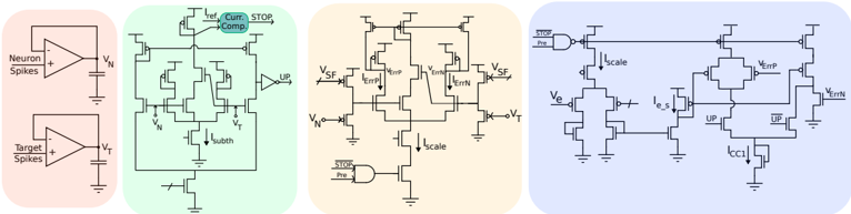
### Visual Description
\n
## Electronic Circuit Diagrams: Neuromorphic Computing Blocks
### Overview
The image presents four electronic circuit diagrams, likely representing building blocks for a neuromorphic computing system. The diagrams appear to illustrate different stages or components involved in processing neuron and target spike signals. The diagrams are arranged horizontally, suggesting a sequential flow of information or processing. Each diagram is contained within a colored rectangular border (red, green, yellow, and blue).
### Components/Axes
The diagrams do not have traditional axes or legends. Instead, they consist of interconnected transistors, operational amplifiers (op-amps), and logic gates. Key labels within the diagrams include:
* **V<sub>N</sub>**: Neuron Spikes (appears in the red diagram)
* **V<sub>T</sub>**: Target Spikes (appears in the red diagram)
* **I<sub>subth</sub>**: Subthreshold Current (appears in the green diagram)
* **Comp**: Comparator (appears in the green diagram)
* **UP**: Operational Amplifier (appears in the green, yellow, and blue diagrams)
* **V<sub>SF</sub>**: Signal Feedback (appears in the yellow diagram)
* **V<sub>ERN</sub>**: Error Neuron (appears in the yellow diagram)
* **V<sub>SE</sub>**: Signal Error (appears in the yellow diagram)
* **Scale**: Scaling factor (appears in the yellow and blue diagrams)
* **STOP**: Stop signal (appears in the yellow diagram)
* **V<sub>E</sub>**: Error Voltage (appears in the blue diagram)
* **I<sub>eS</sub>**: Error Signal Current (appears in the blue diagram)
* **V<sub>ENP</sub>**: Error Neuron Potential (appears in the blue diagram)
* **V<sub>rTN</sub>**: Reset Threshold Neuron (appears in the blue diagram)
* **I<sub>CCI</sub>**: Current Control Input (appears in the blue diagram)
### Detailed Analysis / Content Details
**Diagram 1 (Red):**
This diagram shows two op-amps connected to inputs labeled "Neuron Spikes" (V<sub>N</sub>) and "Target Spikes" (V<sub>T</sub>). Both inputs are connected to ground. This appears to be a differential amplifier configuration.
**Diagram 2 (Green):**
This diagram features a more complex arrangement of transistors. A transistor labeled "I<sub>subth</sub>" is connected to a comparator labeled "Comp". Several transistors are arranged in a feedback loop, with an op-amp labeled "UP" providing amplification.
**Diagram 3 (Yellow):**
This diagram includes multiple transistors and op-amps. Signals labeled "V<sub>SF</sub>" (Signal Feedback) and "V<sub>SE</sub>" (Signal Error) are present. A logic gate labeled "STOP" is also visible, along with a "Scale" input. The diagram also shows "V<sub>ERN</sub>" (Error Neuron).
**Diagram 4 (Blue):**
This diagram is the most complex, with numerous transistors and op-amps. It includes signals labeled "V<sub>E</sub>" (Error Voltage), "I<sub>eS</sub>" (Error Signal Current), "V<sub>ENP</sub>" (Error Neuron Potential), and "V<sub>rTN</sub>" (Reset Threshold Neuron). A "Scale" input and "I<sub>CCI</sub>" (Current Control Input) are also present.
### Key Observations
* The diagrams progressively increase in complexity from left to right.
* The presence of op-amps ("UP") in multiple diagrams suggests amplification and signal processing are key functions.
* The inclusion of "STOP" and "Scale" signals indicates control mechanisms for the circuits.
* The labels related to "Error" (V<sub>ERN</sub>, V<sub>SE</sub>, V<sub>E</sub>, I<sub>eS</sub>, V<sub>ENP</sub>) suggest error correction or learning mechanisms.
* The diagrams are likely designed to mimic the behavior of biological neurons and synapses.
### Interpretation
These diagrams likely represent a series of circuits designed to implement a simplified model of neural computation. The first diagram (red) could be a basic comparator or difference amplifier. The subsequent diagrams (green, yellow, and blue) appear to build upon this foundation, adding features for subthreshold current control, signal feedback, error correction, and scaling. The increasing complexity suggests a hierarchical processing structure, where signals are refined and adjusted as they pass through each stage. The presence of error-related signals indicates a learning or adaptation mechanism, where the circuits can adjust their behavior based on the difference between the neuron's output and a target signal. The overall system is likely intended to perform tasks such as pattern recognition, classification, or control, mimicking the functionality of a biological neural network. The diagrams are not providing specific data points, but rather a schematic representation of a system. The diagrams are a blueprint for a neuromorphic system, and the relationships between the components suggest a flow of information and processing.
</details>
neuromorphic architecture Figure 2 . 2 a illustrates the event-based neuromorphic architecture encompassing the learning algorithm. It consists of a 1 T 1 R array, a Switch Controller,
Leaky Integrate and Fire (I&F) neurons and a learning block (LB). Every neuron receives excitatory and inhibitory currents from two rows of the 1 T 1 R array respectively.
With the arrival of every event through the AER interface (not shown), two consecutive READ and WRITE signals are generated [ 115 ]. Based on these signals, the asynchronous state machine in Fig. 2 . 2 b controls the sequence so that the SLs, BLs and the WLs of the array are driven by the appropriate voltages such that: device is read, its value is integrated by the I&F neuron; the error value is updated through the learning block (LB), generating ICC 1 and ICC 2 (section 2 . 3 ); Based on these values, the excitatory and inhibitory devices are programmed.
learning circuits Based on Alg. 1 and data from Fig. 2 . 1 , we have designed circuits that generate the appropriate ICC , based on the firing rate distance between the neuron and its target. Figure 2 . 3 presents these circuits. The spikes from the neurons and the target are integrated using subthreshold Gm-C filters highlighted in red generating VN and VT . These voltages are subtracted from one another using a subthreshold "Bump" ( subBump ) circuit [ 121 ] highlighted in green, and an above-threshold "Bump" circuit ( abvBump ) in orange.
subBump circuit compares VN and VT giving rise to the error currents when neuron and the target frequencies are far apart and generates the STOP signal when the error is small and in the stop-learning range ( δ th ) [ 120 , 122 ]. STOP signal gates the tail current of all the above-threshold circuits and thus substantially reduce the power consumption when the learning is stopped. Moreover, input events are also used as another gating mechanism. abvBump circuit subtracts VN and VT and scales it to I scale , equal to the maximum ICC required based on Fig. 2 . 1 . Based on the error sign (UP), the scaled error current is summed with or subtracted from the scaled device current generating the desired ICC (Alg. 1 ). This circuit is highlighted in purple.
circuit simulations results Figure 2 . 4 a depicts the positive and negative error currents, STOP-learning signal, and the ICC 1 and ICC 2 currents. The error currents follow a Sigmoid which can be approximated by a line for error values between 1 and 1 . As is explained in Alg. 1 , for positive errors, ICC 2 ( ICC 1 ) follows the summation (subtraction) of the error current with the scaled device current, while for the negative errors, it is the opposite. Figure 2 . 4 b illustrates the dependence of the ICC on the current value of the devices which shifts the error current curve up or down.
## 2 . 5 system -level simulations
We performed SNN simulations with BRIAN 2 [ 123 ] to evaluate the performance of our proposed update scheme, incorporating the device models (see Fig. 2 . 1 ) with stochastic weight changes. Our goal was to achieve a test accuracy comparable to the artificial neural networks trained with backpropagation with Single-precision floating-point format (FP 32 ) precision on the digital hardware.
We evaluated our network on the MNIST handwritten digits dataset [ 124 ] using the first five classes ( 30596 training and 5139 testing images, each 28 × 28 pixels). We trained a fully connected, single-layer spiking network with 784 input LIF neurons and 5 output LIF neurons. Each input image was presented for 100 ms, with pixel intensity encoded as Poisson spikes with a rate of [ 0, 200 ] Hz. At the output layer, spikes were counted per neuron during each stimulus, and the neuron with the maximum firing rate was selected as the network prediction. The error signal was calculated as the difference between low-pass filtered network output spikes and low-pass filtered target spikes, encoded as Poisson spikes at 40 kHz.
We modeled the cycle-to-cycle variability of ICC dependent GLRS conductance using a Gaussian distribution with ICC -dependent mean and standard deviation, as described in Section 2 . 2 . This variability model was applied to all synaptic devices in the simulation, and we achieved the test accuracy of 92 . 68 % after training for three epochs.
F igure 2 . 4 : (a) Error current, STOP learning signal and ICC as a function of the normalized error between the target and the neuron frequencies. (b) Change of the ICC 1 (red) and ICC 2 (blue) as a function of the error and the resistance value of the devices.
<details>
<summary>Image 8 Details</summary>
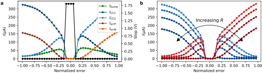
### Visual Description
## Charts: Normalized Error vs. Current/Stop Voltage
### Overview
The image presents two charts (labeled 'a' and 'b') displaying relationships between normalized error and various electrical parameters. Chart 'a' shows current-related parameters (Ibump, ICC1, ICC2, IerrP, IerrN) against normalized error, while chart 'b' shows stop voltage (V) and current (I) against normalized error, with an indication of increasing resistance (R). Both charts share a common x-axis representing normalized error ranging from -1.00 to 1.00.
### Components/Axes
**Common Elements:**
* **X-axis:** Normalized error (ranging from -1.00 to 1.00, with markers at -1.00, -0.75, -0.50, -0.25, 0.00, 0.25, 0.50, 0.75, 1.00)
* **Chart Labels:** 'a' and 'b' to distinguish the two charts.
**Chart 'a':**
* **Y-axis:** Current (µA) with a scale from 0 to 300 µA.
* **Legend:** Located in the top-right corner.
* Ibump (Green, Marker: +)
* ICC1 (Blue, Marker: *)
* ICC2 (Orange, Marker: Δ)
* IerrP (Cyan, Marker: □)
* IerrN (Dark Red, Marker: ◊)
**Chart 'b':**
* **Y-axis:** Stop (V) and Current (µA) - two scales are present. The left scale is for Stop Voltage (V) ranging from 0 to 300 V. The right scale is for Current (µA) ranging from 0 to 300 µA.
* **Annotation:** "Increasing R" with an arrow indicating the direction of increasing resistance.
* **Legend:** No explicit legend is present, but the data series are distinguishable by color and marker. The colors match those in chart 'a'.
### Detailed Analysis or Content Details
**Chart 'a':**
* **Ibump (Green):** The line starts at approximately 300 µA at -1.00 normalized error, decreases steadily to approximately 0 µA at 0.25 normalized error, and remains near 0 µA for the rest of the range.
* **ICC1 (Blue):** The line starts at approximately 300 µA at -1.00 normalized error, decreases steadily to approximately 0 µA at 0.75 normalized error, and remains near 0 µA for the rest of the range.
* **ICC2 (Orange):** The line starts at approximately 175 µA at -1.00 normalized error, decreases to approximately 0 µA at 0.50 normalized error, and remains near 0 µA for the rest of the range.
* **IerrP (Cyan):** The line starts at approximately 0 µA at -1.00 normalized error, increases rapidly to approximately 1.50 µA at 0.00 normalized error, and then decreases to approximately 0 µA at 1.00 normalized error.
* **IerrN (Dark Red):** The line starts at approximately 0 µA at -1.00 normalized error, increases to approximately 0.75 µA at 0.00 normalized error, and then decreases to approximately 0 µA at 1.00 normalized error.
**Chart 'b':**
* The chart displays multiple lines, each representing a different value of resistance (R). The lines generally slope downwards from left to right.
* At -1.00 normalized error, the lines start at approximately 300 µA (current scale) or 300 V (voltage scale).
* As normalized error increases towards 1.00, the lines decrease in both current and voltage.
* The lines with higher resistance (indicated by the "Increasing R" annotation) have steeper slopes.
* The lines converge towards approximately 0 µA and 0 V at 1.00 normalized error.
### Key Observations
* In Chart 'a', Ibump, ICC1, and ICC2 all decrease as normalized error increases, indicating a reduction in these currents with increasing error.
* In Chart 'a', IerrP and IerrN increase initially with normalized error, peaking at 0.00, and then decrease, suggesting an error correction mechanism that is most active around zero error.
* Chart 'b' demonstrates that as resistance increases, the current and stop voltage decrease more rapidly with increasing normalized error.
* The convergence of lines in Chart 'b' at 1.00 normalized error suggests a saturation point or a limit to the system's response.
### Interpretation
The data suggests a system where error correction mechanisms (IerrP and IerrN) are employed to minimize the impact of errors (represented by normalized error). The currents Ibump, ICC1, and ICC2 are affected by the error and decrease as the error increases. Chart 'b' indicates that the system's response is sensitive to resistance, with higher resistance leading to a more pronounced decrease in current and voltage as the error increases.
The "Increasing R" annotation and the associated lines suggest a trade-off between sensitivity and stability. Higher resistance provides greater sensitivity to error but also leads to a more rapid decline in performance as the error increases. The convergence of lines at 1.00 normalized error could represent a point where the system reaches its operational limits or where the error correction mechanisms are no longer effective.
The two charts together provide a comprehensive view of the system's behavior under varying error conditions and resistance levels, highlighting the interplay between these factors and their impact on the system's performance. The data could be used to optimize the system's design by selecting an appropriate resistance value that balances sensitivity and stability.
</details>
## 2 . 6 discussion
Significant effort is underway to develop learning algorithms for SNNs due to their potential for highly parallel, low-power processing. However, a substantial gap exists between these algorithms and their hardware implementation due to noise, variability, and limited bit precision. This gap underscores the importance of technologically plausible learning algorithms rooted in device physics and measurements [ 125 ]. Our work, exploiting ReRAM current compliance ICC for weight updates, represents a step in this direction.
power consumption and scalability While the learning block can generate up to 100 s of µ A s of ICC for large errors, design considerations such as event and STOP-learning signal gating mitigate average power consumption. Peak current per learning block ranges from 1 to 600 µ A , depending on the network error. Leveraging the Poisson distribution of events (due to thermal noise), we can assume that only one column of devices is programmed at a time. Therefore, peak power scales sublinearly with the number of neurons (linear in the worst case). This sublinear scaling implies that power consumption does not fundamentally limit scalability. However, with Poisson-distributed input events and a maximum frequency per input channel, an upper bound for array size exists, determined by event pulse width and tolerance to missing events [ 54 ].
the nonlinear effect The power-law relationship between ICC → GLRS (Fig. 2 . 1 ) introduces a nonlinear mapping of weight updates. This nonlinearity slightly biases the weight update away from the optimal values calculated by the Delta rule. Further investigation into mitigating this bias through calibration or algorithmic compensation could improve learning accuracy.
In this chapter, I presented a technologically plausible learning algorithm that leverages the compliance current of binary ReRAMs to generate variable, multi-level conductance changes. Our comprehensive co-design approach spans multiple levels of abstraction, from device measurements to algorithm, architecture, and circuits. We believe this work represents a significant step toward realizing always-on, on-chip learning systems. As we will see in Chapter 4 , our method can be extended to other non-volatile materials, providing a broader pathway for on-chip learning hardware.
## ONLINE TEMPORAL CREDIT ASSIGNMENT WITH NON-VOLATILE AND VOLATILE MEMRISTORS
This chapter builds upon three conceptually linked works. My initial concept of investigating the online credit assignment problem for recurrent neural networks implemented with non-ideal non-volatile memristive devices [ 126 ], and the subsequent utilization of eligibility traces with volatile memristors for scalability [ 127 ], laid the foundation for this research. These concepts were further validated through real-hardware testing in collaboration with IBM Research Zürich [ 128 ].
## 3 . 1 framework for online training of rsnns with non -volatile memristors
Training RSNNs on ultra-low-power hardware remains a significant challenge. This is primarily due to the lack of spatio-temporally local learning mechanisms capable of addressing the credit assignment problem effectively, especially with limited weight resolution and online training with a batch size of one. These challenges are accentuated when using memristive devices for in-memory computing to mitigate the von Neumann bottleneck, at the expense of increased stochasticity in recurrent computations.
To investigate online learning in memristive neuromorphic Recurrent Neural Network (RNN) architectures, we present a simulation framework and experiments on differential-architecture crossbar arrays based on an accurate and comprehensive PCM device model. We train a spiking RNN on regression tasks, with weights emulated within this framework, using the recently proposed e-prop learning rule. While e-prop truncates the exact gradients to follow locality constraints, its direct implementation on memristive substrates is hindered by significant PCM non-idealities. We compare several widely adopted weight update schemes designed to cope with these non-idealities and demonstrate that only gradient accumulation can enable efficient online training of RSNNs on memristive substrates.
## 3 . 1 . 1 Introduction
RNNs are a remarkably expressive [ 129 ] class of neural networks, successfully adapted in domains such as audio/video processing, language modeling and Reinforcement Learning (RL) [ 130 -135 ]. Their power lies in their architecture, enabling the processing of long and complex sequential data. Each neuron contributes to network processing at various times in the computation, promoting hardware efficiency by the principle of reuse and being the dominant architecture observed in the mammalian neocortex [ 136 , 137 ]. However, training RNNss under constrained memory and computational resources remains a challenge [ 83 ].
Current hardware implementations of neural networks still lag behind the energy efficiency of biological systems, largely due to data movement between separate processing and memory units in von Neumann architectures. Compact nanoscale memristive devices have gained attention for implementing artificial synapses [ 99 , 138 -142 ]. These devices enable calculating synaptic propagation in-memory between neurons, breaking the von Neumann bottleneck [ 92 , 93 ]
Memristive devices are particularly promising for SNNs, especially for low-power, sparse, and event-based neuromorphic systems that emulate biological principles [ 143 , 144 ]. In these systems, synapses (memory) and neurons (processing units) are arranged in a crossbar architecture (Fig. 3 . 1 a), with memristive devices storing synaptic efficacy in their programmable multi-bit conductance values. This architecture inherently supports the sparse, event-driven nature of SNNs, enabling in-memory computation of synaptic propagation through Ohm's and Kirchhoff's Laws. As demonstrated for 32 nm technology [ 145 , 146 ], memristive crossbar arrays offer higher density and lower dynamic energy consumption during inference compared to traditional Static Random Access Memory (SRAM). Additionally, their non-volatile nature reduces static power consumption associated with volatile CMOS memory. Thus, in-memory acceleration of spiking
RNNs with non-volatile, multi-bit resolution memristive devices is a promising path for scalable neuromorphic hardware in temporal signal processing.
PCM devices are among the most mature emerging resistive memory technologies. Their small footprint, fast read/write operation, and multi-bit storage capacity make them ideal for in-memory computation of synaptic propagation [ 147 , 148 ]. Consequently, PCM technology has seen increased interest in neuromorphic computing [ 138 , 149 -151 ].
While a single PCM device can achieve 3 -4 bits of resolution [ 152 ], they exhibit significant non-idealities due to stochastic Joule heating-based switching physics. Molecular dynamics introduce 1/ f noise and structural relaxation, leading to cycle-to-cycle variation in addition to device-to-device variability from fabrication.
Hardware-algorithm co-design with chip-in-the-loop setups is one approach to address these non-idealities [ 138 ]. However, neural network training necessitates iterative evaluation of architectures, learning rule modifications, and hyperparameter tuning on large datasets, which are time and resource-intensive with such setups. In contrast, a software simulation framework with highly accurate statistical model of memristive devices offers faster iteration and better understanding of device effects due to increased observability of internal state variables.
In this work, we investigate whether a RSNN can be trained with a local learning rule despite the adverse impacts of memristive in-memory computing, including write/read noise, conductance drift, and limited bit precision. We build upon the statistical PCM model from Nandakumar et al. [ 81 ] to faithfully model a differential memristor crossbar array (Section 3 . 1 . 3 ), define a target spiking RNN architecture, and describe the properties of an ideal learning rule, selecting the e-prop algorithm [ 75 ] for training (Section 3 . 1 . 3 . 1 ). We implement multiple memristor-aware weight update methods to map ideal e-prop updates to memristor conductances on the crossbar array, addressing device non-idealities (Section 3 . 1 . 3 . 2 ). Finally, we present a training scheme exploiting in-memory computing with extreme sparsity and reduced conductance updates for energy-efficient training (Section 3 . 1 . 3 . 4 ).
## 3 . 1 . 2 Building blocks for training on in-memory processing cores
In this section, we describe the main components of our simulation framework for training spiking RNNs with PCM synapses 1 .
## 3 . 1 . 3 PCM device modeling and integration into neural networks
The nanoscale PCM device typically consists of a Ge2Sb2Te5 (GST) switching material sandwiched between two metal electrodes, forming a mushroom-like structure (Fig. 3 . 1 b). Short electrical pulses applied to the device terminals induce Joule heating, locally modifying the temperature distribution within the PCM. This controlled temperature change can switch the molecular configuration of GST between amorphous (high-resistance) and crystalline (low-resistance) states [ 17 ].
A short, high-amplitude RESET pulse (typically 3 . 5 V amplitude and 20 ns duration) increases the amorphous state volume by melting a significant portion of the GST, which then rapidly quenches to form an amorphous configuration. Conversely, a longer, lower-amplitude SET pulse ( 3 . 5 V amplitude and 20 ns duration) increases the crystalline volume by raising the temperature to initiate crystal nuclei growth. To read the device conductance, a smaller-amplitude READ pulse ( 0 . 2 V amplitude 50 ns duration) is applied to avoid inducing phase transitions.
In practice, PCM programming operations suffer from write/read noise and conductance drift [ 153 ]. The asymmetry of SET and RESET operations, along with the nonlinear conductance response to pulse number and frequency, complicate precise programming. Accurately capturing these non-idealities and device dynamics in network models is crucial for realistic evaluation of metrics such as weight update robustness, hyperparameter choices, and training duration.
While comprehensive models exist for describing PCM electrical [ 45 ], thermal [ 154 ], structural [ 155 , 156 ], and phase-change properties [ 157 , 158 ], these models often involve on-the-fly differential equations with uncertain numerical convergence, lack incorporation of inter- and
1 The code is available at https://github.com/YigitDemirag/srnn-pcm
F igure 3 . 1 : a. PCM devices can be arranged in a crossbar architecture to emulate both a non-volatile synaptic memory and a parallel and asynchronous synaptic propagation using in-memory computation. b. Mushroom-type geometry of a single PCM device. The conductance of the device can be reconfigured by changing the volume ratio of amorphous and crystalline regions.
<details>
<summary>Image 9 Details</summary>
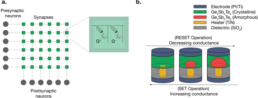
### Visual Description
\n
## Diagram: Neural Network and Memristor Operation
### Overview
The image presents a diagram illustrating a neural network structure alongside a schematic of a memristor device and its operational states. Part (a) depicts a simplified neural network with presynaptic and postsynaptic neurons connected by synapses. Part (b) details the layered structure of a memristor and illustrates the "SET" and "RESET" operations, which correspond to increasing and decreasing conductance, respectively.
### Components/Axes
**Part (a): Neural Network**
* **Labels:** "Presynaptic neurons", "Synapses", "Postsynaptic neurons".
* The diagram shows a grid-like arrangement of neurons. Presynaptic neurons are on the left, postsynaptic neurons on the right, and synapses connect them.
**Part (b): Memristor Operation**
* **Legend:**
* Blue: Electrode (Pt/Ti)
* Green: Ge₂Sb₂Te₅ (Crystalline)
* Red: Ge₂Sb₂Te₅ (Amorphous)
* Yellow: Heater (TiN)
* Gray: Dielectric (SiO₂)
* **Labels:** "(RESET Operation) Decreasing conductance", "(SET Operation) Increasing conductance".
* The diagram shows a cylindrical structure representing the memristor, with layers corresponding to the legend. Two states are depicted: one with a crystalline Ge₂Sb₂Te₅ region (SET) and one with an amorphous Ge₂Sb₂Te₅ region (RESET).
### Detailed Analysis or Content Details
**Part (a): Neural Network**
* There are approximately 8 presynaptic neurons and 8 postsynaptic neurons.
* Each presynaptic neuron appears to connect to each postsynaptic neuron via a synapse.
* The inset shows a simplified circuit diagram with two transistors labeled "G+".
**Part (b): Memristor Operation**
* **Memristor Structure:** The memristor consists of a cylindrical structure with the following layers (from top to bottom): Electrode (Pt/Ti), Ge₂Sb₂Te₅ (Crystalline or Amorphous), Heater (TiN), and Dielectric (SiO₂).
* **RESET Operation:** In the RESET state, the Ge₂Sb₂Te₅ layer is amorphous (red). This corresponds to decreasing conductance.
* **SET Operation:** In the SET state, the Ge₂Sb₂Te₅ layer is crystalline (green). This corresponds to increasing conductance.
* The diagram visually demonstrates the change in the Ge₂Sb₂Te₅ phase as the mechanism for altering the memristor's conductance.
### Key Observations
* The diagram links the concept of a neural network to the physical operation of a memristor.
* The memristor's ability to change its conductance (SET/RESET) is presented as a potential mechanism for implementing synaptic plasticity in artificial neural networks.
* The crystalline/amorphous phase change of Ge₂Sb₂Te₅ is the core principle behind the memristor's functionality.
### Interpretation
The diagram illustrates a potential hardware implementation of artificial synapses using memristors. The neural network diagram (a) represents the computational structure, while the memristor diagram (b) provides a physical mechanism for implementing the synaptic connections and their plasticity. The ability to switch between crystalline and amorphous states in the Ge₂Sb₂Te₅ layer allows the memristor to mimic the behavior of a biological synapse, where the strength of the connection can be modified based on activity. This suggests a pathway towards building more energy-efficient and biologically inspired computing systems. The inset circuit diagram in (a) hints at the electronic control mechanisms involved in modulating the synaptic connections. The diagram highlights the potential of memristive devices to overcome the limitations of traditional CMOS-based neural networks.
</details>
intra-device stochasticity, or are designed for pulse shapes and current-voltage sweeps that do not reflect circuit operating conditions [ 17 ].
Therefore, we adopted the statistical PCM model by Nandakumar et al. [ 81 ], which captures major PCM non-idealities based on measurements from 10 , 000 devices. This model includes nonlinear conductance change with respect to applied pulses, conductance-dependent write and read stochasticity, and temporal drift (Fig. 3 . 2 ). A programming history variable represents the device's nonlinear response to consecutive SET pulses, updated after each pulse. After a new SET pulse, the model samples conductance change ( ∆ G ) from a Gaussian distribution with mean and standard deviation based on programming history and previous conductance. Drift is included using the empirical exponential drift model [ 156 ] G ( t ) = G ( T 0 ) ( t / T 0 ) -v , where G ( T 0 ) is the conductance after a WRITE pulse at time T 0, and G ( t ) is the final conductance after drift. The model also accounts for 1/ f READ noise [ 159 ], which increases monotonically with conductance.
To integrate this model into neural network simulations, we developed a PyTorch-based PCM crossbar array simulation framework [ 107 ]. This framework tracks all simulated PCM devices in the crossbar simultaneously, enabling realistic SET, RESET, and READ operations (implementation details in Section A). Section 3 . 1 . 3 . 3 describes how this framework is used to represent synaptic weights in an RNN.
F igure 3 . 2 : The chosen PCM model from [ 81 ] captures the major device non-idealities. a. The WRITE model enables calculation of the conductance increase with each consecutive SET pulse applied to the device. The band illustrates one standard deviation. b. The READ model enables calculation of 1/ f noise, increasing as a function of conductance. c. The DRIFT model calculates the temporal conductance evolution as a function time. T 0 indicates the time of measurement after the initial programming of the device.
<details>
<summary>Image 10 Details</summary>
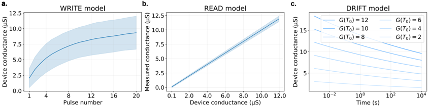
### Visual Description
## Charts: Device Conductance Models (Write, Read, Drift)
### Overview
The image presents three separate charts illustrating different models related to device conductance: a "WRITE" model, a "READ" model, and a "DRIFT" model. Each chart depicts the relationship between conductance and another variable (pulse number, device conductance, and time, respectively). The charts use line plots with shaded areas to represent variability or confidence intervals.
### Components/Axes
**Chart a (WRITE model):**
* **Title:** WRITE model
* **X-axis:** Pulse Number (scale from 0 to 20, approximately)
* **Y-axis:** Device conductance (µS) (scale from 0 to 12.5 µS, approximately)
**Chart b (READ model):**
* **Title:** READ model
* **X-axis:** Device conductance (µS) (scale from 0.1 to 12.0 µS, approximately)
* **Y-axis:** Measured conductance (µS) (scale from 0 to 12.5 µS, approximately)
**Chart c (DRIFT model):**
* **Title:** DRIFT model
* **X-axis:** Time (s) (logarithmic scale, from 10<sup>-2</sup> to 10<sup>4</sup> s, approximately)
* **Y-axis:** Device conductance (µS) (scale from 0 to 16 µS, approximately)
* **Legend:**
* G(T<sub>0</sub>) = 12 (Dark Blue)
* G(T<sub>0</sub>) = 10 (Medium Blue)
* G(T<sub>0</sub>) = 8 (Light Blue)
* G(T<sub>0</sub>) = 6 (Very Light Blue)
* G(T<sub>0</sub>) = 4 (Pale Blue)
* G(T<sub>0</sub>) = 2 (Very Pale Blue)
### Detailed Analysis or Content Details
**Chart a (WRITE model):**
The line representing the WRITE model slopes upward, indicating that device conductance increases with pulse number. The line starts near 0 µS at Pulse Number 0 and reaches approximately 10 µS at Pulse Number 20. A large shaded area surrounds the line, indicating significant variability in the conductance response.
* At Pulse Number 1: ~0.5 µS
* At Pulse Number 4: ~2.5 µS
* At Pulse Number 8: ~5 µS
* At Pulse Number 12: ~7.5 µS
* At Pulse Number 16: ~9 µS
* At Pulse Number 20: ~10 µS
**Chart b (READ model):**
The line in the READ model is nearly linear and slopes upward. It starts near 0 µS at Device Conductance 0.1 µS and reaches approximately 12.5 µS at Device Conductance 12 µS. The shaded area is relatively small, suggesting a more consistent relationship between measured and device conductance.
* At Device Conductance 2 µS: ~2 µS
* At Device Conductance 4 µS: ~4 µS
* At Device Conductance 6 µS: ~6 µS
* At Device Conductance 8 µS: ~8 µS
* At Device Conductance 10 µS: ~10 µS
* At Device Conductance 12 µS: ~12 µS
**Chart c (DRIFT model):**
This chart shows multiple curves, each representing a different initial conductance G(T<sub>0</sub>). All curves slope downward, indicating that device conductance decreases over time. The rate of decrease is faster at shorter time scales and slows down as time increases.
* **G(T<sub>0</sub>) = 12 (Dark Blue):** Starts at ~12 µS and decreases to ~5 µS at 10<sup>4</sup> s.
* **G(T<sub>0</sub>) = 10 (Medium Blue):** Starts at ~10 µS and decreases to ~4 µS at 10<sup>4</sup> s.
* **G(T<sub>0</sub>) = 8 (Light Blue):** Starts at ~8 µS and decreases to ~3 µS at 10<sup>4</sup> s.
* **G(T<sub>0</sub>) = 6 (Very Light Blue):** Starts at ~6 µS and decreases to ~2 µS at 10<sup>4</sup> s.
* **G(T<sub>0</sub>) = 4 (Pale Blue):** Starts at ~4 µS and decreases to ~1 µS at 10<sup>4</sup> s.
* **G(T<sub>0</sub>) = 2 (Very Pale Blue):** Starts at ~2 µS and decreases to ~0.5 µS at 10<sup>4</sup> s.
### Key Observations
* The WRITE model exhibits the most variability in conductance response.
* The READ model shows a strong linear relationship between device and measured conductance.
* The DRIFT model demonstrates that conductance decreases over time, with the initial conductance level influencing the rate of decay.
* The DRIFT model curves appear to asymptotically approach zero conductance as time increases.
### Interpretation
These charts likely represent a model for a memristive device or a similar non-volatile memory element. The WRITE model shows how the device conductance is programmed with successive pulses. The READ model demonstrates the ability to accurately measure the programmed conductance. The DRIFT model illustrates the retention characteristics of the device, showing how conductance degrades over time. The variability in the WRITE model suggests that the writing process is not perfectly controlled, while the linear READ model indicates a reliable measurement process. The DRIFT model is crucial for understanding the long-term stability of the device. The parameter G(T<sub>0</sub>) represents the initial conductance at time zero, and the different curves show how the conductance evolves from different starting points. The logarithmic time scale in the DRIFT model is common for analyzing decay processes. The decreasing conductance over time suggests a gradual loss of stored information, which is a critical factor in memory device design.
</details>
## 3 . 1 . 3 . 1 Credit Assignment Solutions for Recurrent Network Architectures
The credit assignment problem refers to the problem of determining the appropriate change for each synaptic weight to achieve the desired network behavior [ 7 ]. As the architecture determines the information flow inside the network, the credit assignment solution is intertwined with network architecture. Consequently, many proposed solutions in SNNs landscape are specific to architecture components e.g., eligibility traces [ 160 ], dendritic [ 161 ] or neuromodulatory [ 162 ] signals.
In our work, we select a RSNN with LIF neuron dynamics described by the following discretetime equations [ 75 ]:
̸
$$v _ { j } ^ { t + 1 } & = \alpha v _ { j } ^ { t } + \sum _ { i \neq j } W _ { j i } ^ { r e c } z _ { i } ^ { t } + \sum _ { i } W _ { j i } ^ { i n } x _ { i } ^ { t } - z _ { j } ^ { t } v _ { t h } \\ & z _ { j } ^ { t } = H \left ( \frac { v _ { j } ^ { t } - v _ { t h } } { v _ { t h } } \right )$$
where v t j is the membrane voltage of neuron j at time t . The output state of a neuron is a binary variable, z t j , that can either indicate a spike, 1, or no spike, 0. The neuron spikes when the membrane voltage exceeds the threshold voltage vth , a condition that is implemented based on the Heaviside function H . The parameter α ∈ [ 0, 1 ] is the membrane decay factor calculated as α = e -δ t / τ m , where δ t is the discrete time step resolution of the simulation and τ m is the neuronal membrane decay time constant, typically tens of milliseconds. The network activity is driven by input spikes x t i . Input and recurrent weights are represented as W in ji and W rec ji respectively. At the output layer, the recurrent spikes are fed through readout weights W out kj into a single layer of leaky integrator units yk with the decay factor κ ∈ [ 0, 1 ] . This continuous valued output unit is analogous to a motor function which generates coherent motor output patterns [ 163 ] of the type shown in Fig. 3 . 3 .
Training goal is to find optimal network weights { W inp ji , W rec ji and W out kj } , that maximize the task performance [ 7 ]. For an ideal neuromorphic hardware, the learning algorithm must (i) use spatio-temporally local signals (ii) be online and (iii) tested beyond the toy problems. As an example, FORCE algorithm [ 163 , 164 ] performs well on motor tasks, but it violates the first requirement by requiring knowledge of all synaptic weights. BPTT with surrogate gradients [ 165 , 166 ] has its own drawbacks due to the need to buffer intermediate neuron states and activations, violating the second requirement.
E-prop offers a local and online learning rule for single-layer RNNs [ 75 ] by factorizing the gradients into a sum of products between instantaneously available learning signals and local eligibility traces. Speficially, the gradient dE dWji is represented as a sum of products over time t :
$$\frac { d E } { d W _ { j i } } = \sum _ { t } \frac { d E } { d z _ { j } ^ { t } } \cdot \left [ \frac { d z _ { j } ^ { t } } { d W _ { j i } } \right ] _ { l o c a l } \, ,$$
where E is the loss term such as the mean squared error between the network output y t k and target y ∗ , t k for regression tasks.
The term [ dz t j dWji ] local is not an approximation. It is computed locally, carries the factorization of the gradient (a local measure of the the synaptic weight's contribution to the neuronal activity) forward in time, and is described as the eligibility trace for the synapse from neuron i to neuron j at time t . Ideally, the term dE dz t j would be the total derivative of the loss function with respect to the neuron's spike output. However, this is unavailable online as it requires information about the spike's future impact on the error. Therefore, e-prop approximates the learning signal using the partial derivative ∂ E ∂ z t j , considering only the direct influence of the spike output on
the instantaneous error. This approximation enables e-prop to function as an online learning algorithm for RSNNs, at the cost of truncating the exact gradients.
E-prop's performance is notable, achieving performance comparable results to Long Short-Term Memory (LSTM) networks [ 167 ] trained with BPTT on complex temporal tasks. While the OSTL algorithm [ 84 ] also supports complex recurrent architectures and generates exact gradients, its computational complexity makes it less suitable for hardware implementation compared to e-prop.
In this work, we focus on e-prop due to its
- Sufficient gradient alignment: while not exact, e-prop provides a sufficient approximation of the true gradient.
- Relative simplicity: computational locality and simplicity are well-suited for low-power neuromorphic hardware applications.
- Neuroscientific relevance: the employment of eligibility traces aligns with neuroscientific observations of synaptic plasticity.
## 3 . 1 . 3 . 2 Memristor-Aware Weight Update Optimization
In mixed-signal neuromorphic processors, Learning Blocks (LBs) are typically located with neuron circuits [ 143 , 168 , 169 ]. LBs continuously monitor signals available to the neuron (e.g., presynaptic activities, inference, feedback) and, based on the desired learning rule, instruct weight updates on the synapses. However, when network weights are implemented with memristive devices, weight updates are subject to analog non-idealities. Therefore, LB design must consider these device non-idealities, such as programming noise and asymmetric SET/RESET updates, to ensure accurate transfer of calculated gradients to device conductances. To save both energy and area, weight updates are typically implemented in a single-shot fashion, using one or multiple gradual SET pulses to update the device without requiring a read-verify cycle.
In the following, we describe four widely adopted weight update methods for LBs, implemented in our PCM crossbar array simulation framework. Each method is designed to cope with device non-idealities. In all experiments, our framework employs differential synaptic configuration [ 81 , 109 , 110 ], where each synapse has two sets of memristors ( G + and G -) whose difference represents the effective synaptic conductance (Fig. 3 . 1 a) 2
the sign gradient descent ( signgd ) In SignGD, synaptic weights W is updated based solely on the sign of the loss function gradient with respect to the weights, ˆ ∇ W L , as approximated by the online learning rule. Updates only occur when the magnitude of the gradient for a weight exceeds a predefined threshold θ such that
$$\Delta W = - \delta \, s i g n ( \hat { \nabla } _ { W } \mathcal { L } ) \odot \mathbb { I } ( | \hat { \nabla } _ { W } \mathcal { L } | > \theta ) & & ( 3 . 3 )$$
where δ is a positive stochastic variable representing the conductance change due to a single SET pulse applied to the memristor, sign ( · ) is the element-wise sign function, ⊙ is Hadamard product, I ( · ) is the indicator function implementing stop-learning regime ( 1 if true, 0 otherwise).
This approach ensures convergence under certain conditions [ 171 ]. Due to its simplicity, SignGD is popular in memristive neuromorphic systems [ 172 -174 ]. Upon weight update onset, LB applies a single SET pulse to either the G + or the G -PCM device, as determined by the gradient's sign. The effective value of δ is not constant due to WRITE noise and can lead to biases in the weight update distribution, potentially impacting learning dynamics and convergence.
2 In differential configuration, unidirectional updates can saturate one or both devices [ 81 , 109 , 110 ]. While push-pull mechanism [ 170 ] can address this issue in memristors with symmetric SET/RESET characteristics, it's not feasible in PCMs since the abrupt nature of RESET operations [ 46 ]. This necessiates a frequent saturation check and refresh mechanism to reset and reprogram both memristors.
stochastic update ( su ) Conventional optimization methods often require weight updates that are 3 -4 orders of magnitude smaller than the original weight values [ 175 ], posing a challenge for PCM devices with limited precision [ 176 ]. To bridge this precision gap, SU stochastically executes updates based on the approximated gradient's magnitude [ 81 ]:
$$P ( \ u p d a t e ) = \min \left ( 1 , \frac { | \hat { \nabla } _ { W } \mathcal { L } | } { p } \right ) \quad ( 3 . 4 )$$
where p is a scaling factor controlling the update probability. Choosing p such that update probability P ( update ) is proportional to ∥ ˆ ∇ W L∥ ensures that larger gradients are more likely to trigger updates, effectively adapting the learning rate to the limited precision of PCM devices.
In our implementation, we scale the gradient by 1/ p before comparing it to a random uniform value to determine whether an update occurs. This approach, inspired by Nandakumar et al. [ 81 ], allows for fine-grained control over the effective learning rate. Unlike the original work, we perform the refresh operation before the update to prevent updates on saturated devices. This modification further enhances the stability and reliability of the learning process.
multi -memristor update ( mmu ) MMUenhances synaptic weight resolution and mitigates write noise by utilizing 2 N PCM devices per synapse, arranged in N differential pairs [ 109 ]. Updates are applied sequentially to these devices, effectively reducing the minimum achievable weight change by a factor of 2 N and the variance due to write noise by a factor of √ 2 N (see Supplementary Note 3 ).
In our implementation, we estimate the number of SET pulses required to achieve the desired conductance change, assuming a linear conductance increase of 0 . 75 µ S per pulse (see Section 3 . 1 . 3 ). 3 These pulses are then applied sequentially to the PCM devices in a circular queue. A refresh operation is performed if the conductance of any device pair exceeds 9 µ S and their difference is less than 4 . 5 µ S. This refresh mechanism helps maintain the dynamic range of the synaptic weights and ensures reliable long-term operation.
mixed -precision update ( mpu ) MPUaddresses the discrepancy between the high precision of learning algorithms and the limited resolution of PCM devices by accumulating gradients on a high-precision co-processor until they reach a threshold that can be reliably represented in PCM. This approach is analogous to quantization-aware training techniques [ 110 , 111 ].
In our implementation, approximated gradients calculated by e-prop are accumulated in FP 32 memory until they are an integer multiple of the PCM update granularity ( 0.75 µ S). These accumulated values are then converted to the corresponding number of pulses and applied to the PCM devices. A refresh operation is triggered when the conductance of either device in a pair exceeds 9 µ S, and their difference is less than 4.5 µ S, maintaining synaptic efficacy and preventing saturation.
## 3 . 1 . 3 . 3 Training a Spiking RNN on a PCM Crossbar Simulation Framework
We used PCM crossbar array model to determine realistic values for the network parameters { W in ji , W rec ji and W out kj } . To represent synaptic weights, W ∈ [ -1, 1 ] , with PCM device conductance values, G ∈ [ 0.1, 12 ] µ S [ 81 ], we used the linear relationship W = β [ ∑ N G + -∑ N G -] , where ∑ N G + and ∑ N G -are the total conductance of N memristors 4 representing the potentiation and the depression of the synapse respectively [ 81 ].
The forward computation (inference) of Eq. 3 . 1 is simulated using the PCM crossbar simulation framework, incorporating the effects of READ noise and temporal conductance drift. Subsequently, the weight updates calculated by the e-prop algorithm are applied to the PCM-based crossbar arrays using each of the methods described in Section 3 . 1 . 3 . 2 .
3 For a more precise pulse estimation method, refer to Nandakumar et al. [ 81 ].
4 N = 1 for all weight update methods, except multi-memristor updates.
F igure 3 . 3 : Overview of the spiking RNN training framework with the proposed PCM crossbar array simulation framework, illustrated for a pattern generation task. Network weights are allocated from three crossbar array models, Ginp , Grec , Gout . The network-generated pattern is compared to the target pattern to produce a learning signal, which is fed back to each neuron. The LB calculates instantaneous weight changes ∆ W using the e-prop learning rule and has to efficiently transfer the desired weight change to a conductance change, i.e. ∆ W → ∆ G , while accounting for PCM non-idealities.
<details>
<summary>Image 11 Details</summary>
### Visual Description
\n
## Diagram: Recurrent Neural Network with Learning Block
### Overview
This diagram illustrates the architecture of a recurrent neural network (RNN) with a learning block, showing the flow of information and gradients during training. The diagram depicts input neurons, recurrent neurons, output units, generated patterns, and a learning block that adjusts weights based on network loss. The diagram uses arrows to indicate the direction of information flow and dashed arrows to indicate gradient flow.
### Components/Axes
The diagram consists of the following components:
* **Input Neurons:** Represented as a vertical stack of circles on the left.
* **Recurrent Neurons:** A circular arrangement of nodes with interconnections, positioned centrally.
* **Output Unit:** A single circle on the right.
* **G<sub>inp</sub>:** A grid-like structure representing the input to the recurrent neurons.
* **G<sub>rec</sub>:** A grid-like structure representing the recurrent connections.
* **G<sub>out</sub>:** A grid-like structure representing the output from the recurrent neurons.
* **Learning Block:** A rectangular block on the top-right, labeled "Learning Block" and "Per Neuron".
* **Network Loss:** A box containing a wavy line, labeled "Network Loss".
* **Target Pattern:** A box containing a wavy line, labeled "Target Pattern".
* **Generated Pattern:** A box containing a wavy line, labeled "Generated Pattern".
* **ΔG<sub>inp</sub>, ΔG<sub>rec</sub>, ΔG<sub>out</sub>:** Labels indicating gradient changes for input, recurrent, and output grids, respectively.
* **ΔW → ΔG:** Equation within the Learning Block, indicating weight change leading to gradient change.
### Detailed Analysis or Content Details
The diagram shows the following information flow:
1. **Input to Recurrent Neurons:** Input Neurons feed into G<sub>inp</sub>, which then connects to the Recurrent Neurons.
2. **Recurrent Connections:** The Recurrent Neurons have internal connections represented by G<sub>rec</sub>, creating a feedback loop.
3. **Output from Recurrent Neurons:** The Recurrent Neurons output to G<sub>out</sub>, which then connects to the Output Unit.
4. **Pattern Generation:** The Output Unit generates a pattern.
5. **Loss Calculation:** The Generated Pattern is compared to the Target Pattern, resulting in Network Loss.
6. **Gradient Flow:** The Network Loss drives gradient changes (ΔG<sub>out</sub>) back through G<sub>out</sub> to the Recurrent Neurons.
7. **Recurrent Gradient:** The gradient flows through the recurrent connections (ΔG<sub>rec</sub>).
8. **Input Gradient:** The gradient also flows back to the input (ΔG<sub>inp</sub>).
9. **Learning Block:** The gradients (ΔG) are used in the Learning Block to adjust the weights (ΔW).
The Learning Block contains the equation "ΔW → ΔG", indicating that changes in weights (ΔW) lead to changes in gradients (ΔG).
### Key Observations
* The diagram emphasizes the feedback loop inherent in recurrent neural networks through the recurrent connections (G<sub>rec</sub>).
* The gradient flow is depicted as dashed arrows, indicating that it's a process of backpropagation.
* The Learning Block highlights the weight adjustment mechanism based on the network loss.
* The grid-like structures (G<sub>inp</sub>, G<sub>rec</sub>, G<sub>out</sub>) likely represent weight matrices or activation patterns.
### Interpretation
This diagram illustrates the core principles of training a recurrent neural network. The network learns by comparing its generated output to a target pattern and adjusting its weights to minimize the network loss. The recurrent connections allow the network to maintain a "memory" of past inputs, making it suitable for processing sequential data. The gradient flow, facilitated by backpropagation, is crucial for updating the weights and improving the network's performance. The diagram effectively visualizes the complex interplay between input, recurrent connections, output, loss calculation, and weight adjustment in an RNN. The use of grids (G<sub>inp</sub>, G<sub>rec</sub>, G<sub>out</sub>) suggests a matrix-based representation of the network's connections and activations, common in deep learning implementations. The diagram is a conceptual representation and doesn't provide specific numerical values or detailed algorithmic steps, but it effectively conveys the fundamental architecture and training process of an RNN.
</details>
T able 3 . 1 : Performance evaluation of spiking RNNs with models of PCM crossbar arrays.
| Method | Sign-gradient | Stochastic | Multi-mem (N= 4 ) | Multi-mem (N= 8 ) | Mixed-precision |
|----------|-----------------|--------------|---------------------|---------------------|-------------------|
| MSE Loss | 0 . 2080 | 0 . 1808 | 0 . 1875 | 0 . 1645 | 0 . 0380 |
## 3 . 1 . 3 . 4 Results
We validated online training on a 1 D continual pattern generation task [ 75 ], relevant for motor control and value function estimation in RL [ 163 ], using our analog crossbar framework (see Section 3 . 1 . 3 . 5 )
Table 3 . 1 summarizes the training performance of the RSNN using different weight update methods on PCM crossbar arrays. We defined an MSE loss of < 0 . 1 as the performance performance threshold for this task (see Section A for selection criteria). Among the five configurations, only the mixed-precision approach achieved this threshold, demonstrating sparse spiking activity and successful pattern generation.
During training, the weight saturation problem due to the differential configuration is rare ( < 1% ) , as shown in Fig 3 . 5 (right). We hypothesize that this is due to the mixed-precision algorithm reducing the total number of WRITE pulses through update accumulation ( ∼ 12 WRITE pulses are applied per epoch, Fig. 3 . 6 .). Fig. 3 . 5 (left) illustrates the effective weight distribution of the PCM synapses at the end of the training.
To assess performance loss due to PCM non-idealities (WRITE/READ noise, drift), we simulated an ideal 4 -bit device model, effectively acting as a digital 4 -bit memory (Section A).
Table 3 . 2 summarizes the performance of different update methods with this ideal model. Stochastic, multi-memristor ( N = 8), and mixed-precision updates successfully solved the task, with mixed-precision achieving the best accuracy. All methods performed better without PCM non-idealities. Interestingly, stochastic updates outperformed both multi-memristor methods, suggesting the importance of few stochastic updates when training with quantized weights.
To further evaluate the impact of limited bit precision, we trained the same network with e-prop using standard FP 32 weights. This high-resolution training yielded comparable results to mixed-precision training with either ideal quantized memory or the PCM cell model.
<details>
<summary>Image 12 Details</summary>
### Visual Description
## Charts/Graphs: Recurrent Neural Network Training and Spike Patterns
### Overview
The image presents a series of charts illustrating the training process and output patterns of a recurrent neural network (RNN). The top chart displays the spike patterns of neurons in the recurrent layer over time. The bottom-left chart shows the training loss as a function of epoch. The bottom-right charts show pattern generation, comparing the target output with the RNN output over time for three different patterns.
### Components/Axes
* **Top Chart:**
* Title: "Recurrent layer spike patterns"
* X-axis: "Time (ms)", ranging from 0 to 900, with markers every 100 ms.
* Y-axis: "Neuron ID", ranging from 0 to 100, with markers every 25.
* Data: Blue vertical lines representing spike events for individual neurons at specific times.
* **Bottom-Left Chart:**
* Title: "Training Loss"
* X-axis: "Epoch", ranging from 0 to 250, with markers every 50.
* Y-axis: "Loss", ranging from 0.10 to 0.30, with markers every 0.05.
* Data: A blue line representing the training loss over epochs, with a shaded region indicating the standard deviation.
* **Bottom-Right Charts (3 subplots):**
* Title: "Pattern Generation"
* X-axis: "Time (ms)", ranging from 0 to 1000, with markers every 200.
* Y-axis: "Output", ranging from -2 to 2, with markers every 0.5.
* Data:
* Blue line: "Target" output pattern.
* Orange line: "RNN output" pattern.
* Legend: Located in the top-right corner of the first subplot, labeling the blue line as "Target" and the orange line as "RNN output".
### Detailed Analysis or Content Details
* **Top Chart:** The spike patterns appear somewhat random, with varying densities of spikes across different neurons and time intervals. There are periods of higher activity (more spikes) and periods of relative silence. The distribution of spikes seems fairly uniform across the neuron IDs.
* **Bottom-Left Chart:** The training loss initially decreases rapidly from approximately 0.27 at epoch 0 to around 0.16 at epoch 50. After epoch 50, the loss decreases more slowly, with fluctuations. At epoch 250, the loss is approximately 0.13. The shaded region indicates a relatively large standard deviation, suggesting some variability in the training process.
* **Bottom-Right Charts:**
* **Subplot 1:** The RNN output (orange line) closely follows the target output (blue line) throughout the entire time range. There is a slight phase shift, with the RNN output lagging behind the target output.
* **Subplot 2:** Similar to subplot 1, the RNN output closely tracks the target output, with a slight lag.
* **Subplot 3:** The RNN output again follows the target output, but with a more noticeable difference in amplitude. The RNN output appears to be slightly dampened compared to the target output.
### Key Observations
* The training loss decreases significantly during the initial epochs, indicating that the RNN is learning quickly.
* The spike patterns in the recurrent layer are complex and dynamic.
* The RNN is able to generate patterns that closely resemble the target patterns, but there are some discrepancies in timing and amplitude.
* The standard deviation of the training loss is relatively high, suggesting that the training process is not entirely stable.
### Interpretation
The data suggests that the RNN is successfully learning to generate the desired output patterns. The decreasing training loss indicates that the network is improving its ability to predict the target outputs. The spike patterns in the recurrent layer likely represent the internal representations that the network is using to encode and process information. The discrepancies between the target and RNN outputs suggest that there is still room for improvement in the network's performance. The high standard deviation of the training loss could be due to factors such as the complexity of the task, the size of the training dataset, or the choice of hyperparameters.
The RNN is demonstrating an ability to learn temporal dependencies, as evidenced by its ability to generate patterns that evolve over time. The comparison between the target and RNN outputs provides insights into the network's strengths and weaknesses. The observed lag in the RNN output could be due to the inherent delay in processing information through the recurrent connections. The dampened amplitude in the third subplot could be due to the network's tendency to regularize its outputs. Overall, the data suggests that the RNN is a promising approach for modeling and generating complex temporal patterns.
</details>
F igure 3 . 4 : Dynamics of a network trained with the mixed-precision algorithm. The raster plot (top) shows the sparse spiking activity ( ∼ 3 . 3 Hz) of recurrent-layer neurons. The training loss (bottom left) demonstrates MSE loss over 250 epochs is averaged over ten best network hyperparameters (see Fig A. 8 for the best performing hyperparameter). Properly-tuned neuronal time constants and trained network weights result in generated patterns following the targets (bottom right). The generated patterns are extracted from three different spiking RNNs.
F igure 3 . 5 : (left) The effective conductance distributions ( G + -G -) of the synapses in the input, recurrent and output layer, at the end of the training with the mixed-precision method. (right) Averaged over 50 training runs, the mean number of PCM devices requiring a refresh is shown for each layer. The refresh operation was not needed for recurrent and output layers.
<details>
<summary>Image 13 Details</summary>
### Visual Description
\n
## Charts: Conductance Distribution and PCM Count over Epochs
### Overview
The image presents two charts. The left chart displays histograms of effective conductance for three layers: Input (Inp), Reconstruction (Rec), and Output (Out). The right chart shows the number of Phase Change Memory (PCM) elements as a function of epoch, also separated by layer.
### Components/Axes
**Left Chart (Histograms):**
* **X-axis:** Effective conductance (µS), ranging from approximately -10 to 10.
* **Y-axis:** Count, displayed on a logarithmic scale from 10⁰ to 10³.
* **Layers:** Inp layer (light blue), Rec layer (purple), Out layer (dark purple).
**Right Chart (PCM Count vs. Epoch):**
* **X-axis:** Epoch, ranging from approximately 50 to 250.
* **Y-axis:** Number of PCMs, ranging from 0 to 0.55.
* **Layers:** Inp layer (light blue), Rec layer (grey), Out layer (dark purple).
* **Shaded Area:** Represents the standard deviation around each line.
### Detailed Analysis or Content Details
**Left Chart (Histograms):**
* **Inp Layer (light blue):** The distribution is heavily concentrated around an effective conductance of approximately 2 µS. The count at this peak is around 800. The distribution is relatively narrow.
* **Rec Layer (purple):** The distribution is wider and more spread out, with multiple peaks. The most prominent peaks are around -3 µS and 3 µS, each with a count of approximately 1000. There are smaller peaks around -6 µS and 6 µS.
* **Out Layer (dark purple):** The distribution is concentrated around an effective conductance of approximately 0 µS. The count at this peak is around 1000. The distribution is relatively narrow.
**Right Chart (PCM Count vs. Epoch):**
* **Inp Layer (light blue):** The line starts at approximately 0.03 at epoch 50 and increases to approximately 0.23 at epoch 250. The line slopes upward, with a steeper increase between epochs 150 and 200.
* **Rec Layer (grey):** The line starts at approximately 0.02 at epoch 50 and increases to approximately 0.18 at epoch 250. The line slopes upward, with a more gradual increase than the Inp layer.
* **Out Layer (dark purple):** The line starts at approximately 0.01 at epoch 50 and increases to approximately 0.20 at epoch 250. The line slopes upward, with a similar rate of increase to the Rec layer.
### Key Observations
* The Inp layer exhibits a highly concentrated conductance distribution around 2 µS.
* The Rec layer shows a broader distribution with multiple conductance peaks, suggesting a more diverse range of conductance values.
* The Out layer's conductance is centered around 0 µS.
* The number of PCMs increases with epoch for all three layers, indicating a learning or adaptation process.
* The Inp layer shows the fastest increase in PCM count over epochs.
* The shaded areas indicate the uncertainty in the PCM count, which appears to be relatively consistent across epochs.
### Interpretation
The data suggests that the different layers of the network exhibit distinct conductance characteristics. The Inp layer appears to be primarily responsible for transmitting signals with a specific conductance value, while the Rec layer handles a wider range of conductance values, potentially enabling more complex processing. The Out layer's conductance being centered around 0 µS could indicate its role in decision-making or thresholding.
The increase in PCM count over epochs for all layers suggests that the network is learning and adapting its conductance values to improve performance. The faster increase in PCM count for the Inp layer could indicate that this layer is undergoing more significant changes during the learning process. The standard deviation around the PCM count lines suggests that the learning process is relatively stable and consistent.
The differing distributions of conductance values across layers likely reflect the specific functions each layer performs within the neural network. The Inp layer's narrow distribution suggests a specialized role, while the Rec layer's broader distribution suggests a more versatile role. The Out layer's distribution around 0 µS suggests a role in signal gating or activation.
</details>
F igure 3 . 6 : Total number of WRITE pulses applied to PCM devices are shown for the input, recurrent and output layers. Only 0 . 07 %, 0 . 07 % and 0 . 1 % of PCM devices within each layer are programmed respectively during mixed-precision training.
<details>
<summary>Image 14 Details</summary>
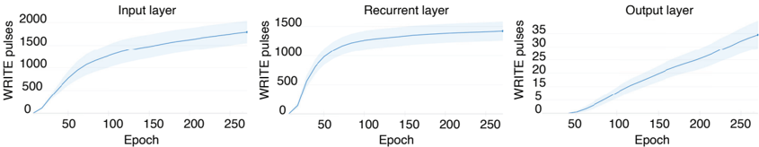
### Visual Description
\n
## Line Charts: WRITE pulses vs. Epoch for Neural Network Layers
### Overview
The image presents three line charts, arranged horizontally. Each chart depicts the relationship between "WRITE pulses" (y-axis) and "Epoch" (x-axis) for a different layer of a neural network: Input layer, Recurrent layer, and Output layer. Each line chart also includes a shaded region around the line, likely representing a standard deviation or confidence interval.
### Components/Axes
* **X-axis (all charts):** "Epoch", ranging from approximately 0 to 250. The axis is labeled with numerical markers at intervals of 50.
* **Y-axis (Input & Recurrent layers):** "WRITE pulses", ranging from 0 to 2000 (Input) and 0 to 1500 (Recurrent). The axis is labeled with numerical markers at intervals of 500.
* **Y-axis (Output layer):** "WRITE pulses", ranging from 0 to 35. The axis is labeled with numerical markers at intervals of 5.
* **Chart Titles:** "Input layer", "Recurrent layer", "Output layer" positioned above each respective chart.
* **Data Series:** Each chart contains a single blue line representing the average "WRITE pulses" over epochs, with a light blue shaded area indicating the variance.
### Detailed Analysis or Content Details
**Input Layer:**
* The line slopes upward, indicating an increase in WRITE pulses with increasing epochs.
* At Epoch 50, WRITE pulses are approximately 100.
* At Epoch 100, WRITE pulses are approximately 500.
* At Epoch 150, WRITE pulses are approximately 1000.
* At Epoch 200, WRITE pulses are approximately 1500.
* At Epoch 250, WRITE pulses are approximately 1900.
* The shaded region is wider at higher epochs, suggesting greater variance in WRITE pulses.
**Recurrent Layer:**
* The line also slopes upward, but the initial increase is more rapid than in the Input layer.
* At Epoch 50, WRITE pulses are approximately 200.
* At Epoch 100, WRITE pulses are approximately 700.
* At Epoch 150, WRITE pulses are approximately 1200.
* At Epoch 200, WRITE pulses are approximately 1400.
* At Epoch 250, WRITE pulses are approximately 1500.
* The shaded region is relatively consistent across epochs.
**Output Layer:**
* The line slopes upward, but the increase is slower and the absolute values are much lower than the other two layers.
* At Epoch 50, WRITE pulses are approximately 2.
* At Epoch 100, WRITE pulses are approximately 8.
* At Epoch 150, WRITE pulses are approximately 15.
* At Epoch 200, WRITE pulses are approximately 25.
* At Epoch 250, WRITE pulses are approximately 32.
* The shaded region is wider at higher epochs, similar to the Input layer.
### Key Observations
* All three layers exhibit a positive correlation between Epoch and WRITE pulses.
* The Recurrent layer shows the most rapid initial increase in WRITE pulses.
* The Output layer has significantly lower WRITE pulse values compared to the Input and Recurrent layers.
* The variance in WRITE pulses appears to increase with the number of epochs for the Input and Output layers.
### Interpretation
The charts demonstrate how the number of WRITE pulses changes over the training process (epochs) for different layers of a neural network. WRITE pulses likely represent a measure of activity or updates within each layer. The differing rates of increase and absolute values suggest that each layer learns and processes information at a different pace and scale. The increasing variance at higher epochs for the Input and Output layers could indicate that the learning process becomes more unstable or less predictable as training progresses. The lower WRITE pulse values in the Output layer might suggest that this layer requires less frequent updates or has a different role in the network's overall function. The data suggests that the network is learning, as evidenced by the increasing WRITE pulses in all layers, but the learning dynamics differ significantly between layers.
</details>
T able 3 . 2 : Performance evaluation of spiking RNNs with an ideal crossbar array model 5
| Method | Sign-gradient | Stochastic | Multi-mem (N= 4 ) | Multi-mem (N= 8 ) | Mixed-precision |
|----------|-----------------|--------------|---------------------|---------------------|-------------------|
| MSE Loss | 0 . 1021 | 0 . 0758 | 0 . 1248 | 0 . 0850 | 0 . 0289 |
Similar to Nandakumar et al. [ 81 ], we found that the probability scaling factor p in the stochastic update method allows tuning the number of devices programmed during training. Figure 3 . 7 shows that increasing p (decreasing update probability) can reduce WRITE pulses by up to an order of magnitude without degrading the loss. This result highlights the potential for optimizing energy efficiency in memristive online learning systems by strategically adjusting the update probability.
F igure 3 . 7 : The stochastic update method enables tuning the number of WRITE pulses to be applied to PCM devices.
<details>
<summary>Image 15 Details</summary>
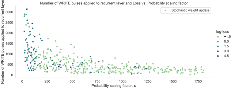
### Visual Description
## Scatter Plot: Number of WRITE pulses vs. Probability scaling factor
### Overview
This image presents a scatter plot illustrating the relationship between the number of WRITE pulses applied to a recurrent layer and the probability scaling factor (p). The plot also visualizes the log-loss associated with different combinations of these two parameters. The data points are color-coded based on their log-loss values.
### Components/Axes
* **Title:** "Number of WRITE pulses applied to recurrent layer and Loss vs. Probability scaling factor" (Top-center)
* **X-axis:** "Probability scaling factor, p" (Bottom-center), ranging from approximately 0 to 1750.
* **Y-axis:** "Number of WRITE pulses applied to recurrent layer" (Left-center), ranging from approximately 0 to 3000.
* **Legend:** Located in the top-right corner, labeled "log-loss" with the following color-coded values:
* -1.5 (Dark Blue)
* 0.0 (Medium Blue)
* 3.0 (Light Green)
* 4.5 (Dark Green)
* **Annotation:** "Stochastic weight update" (Top-right, near the legend)
### Detailed Analysis
The scatter plot shows a general trend of decreasing WRITE pulses as the probability scaling factor increases. The data points are clustered based on their log-loss values.
* **Log-loss -1.5 (Dark Blue):** These points are concentrated at low probability scaling factors (p < 100) and high numbers of WRITE pulses (1000-3000). The trend is a steep decline in WRITE pulses as p increases. Approximate data points: (0, 2800), (10, 2200), (50, 1200), (100, 800).
* **Log-loss 0.0 (Medium Blue):** These points are more dispersed, spanning a wider range of probability scaling factors (p < 500) and WRITE pulses (500-2500). The trend is a gradual decrease in WRITE pulses as p increases. Approximate data points: (0, 1800), (50, 1500), (200, 1000), (400, 600).
* **Log-loss 3.0 (Light Green):** These points are primarily located in the middle range of probability scaling factors (p between 200 and 1000) and lower WRITE pulses (0-1500). The trend is relatively flat, with some fluctuation. Approximate data points: (200, 800), (500, 500), (800, 300).
* **Log-loss 4.5 (Dark Green):** These points are scattered across the entire range of probability scaling factors (p between 0 and 1750) and have the lowest WRITE pulse counts (0-500). The trend is a slight decrease in WRITE pulses as p increases. Approximate data points: (0, 200), (500, 100), (1000, 50), (1500, 100).
### Key Observations
* Lower log-loss values (better performance) are associated with lower probability scaling factors and higher numbers of WRITE pulses.
* As the probability scaling factor increases, the number of WRITE pulses generally decreases.
* The distribution of points with log-loss 3.0 and 4.5 is more spread out, indicating a wider range of possible outcomes for these loss values.
* There is a clear separation between the data points based on log-loss, suggesting that log-loss is a strong predictor of the relationship between WRITE pulses and the probability scaling factor.
### Interpretation
The data suggests that the number of WRITE pulses applied to the recurrent layer and the probability scaling factor are key parameters influencing the performance of the model, as measured by log-loss. A lower probability scaling factor and a higher number of WRITE pulses appear to lead to better performance (lower log-loss). The "Stochastic weight update" annotation suggests that this relationship may be influenced by the stochastic nature of the weight updates during training. The plot demonstrates a trade-off between the probability scaling factor and the number of WRITE pulses – increasing one generally decreases the other. The clustering of points based on log-loss indicates that there are distinct regions of parameter space that result in different levels of performance. The spread of points with higher log-loss values suggests that the model is more sensitive to changes in these parameters when performance is suboptimal. This data could be used to optimize the training process by selecting appropriate values for the probability scaling factor and the number of WRITE pulses.
</details>
## 3 . 1 . 3 . 5 Methods
For the chosen pattern generation task, the network consists of 100 input and 100 recurrent LIF neurons, along with one leaky-integrator output unit. The network receives a fixed-rate Poisson input, and the target pattern is a one-second-long sequence defined as the sum of four sinusoids ( 1 Hz, 2 Hz, 3 Hz and 5 Hz), with phases and amplitudes are randomly sampled from uniform distributions [ 0, 2 π ] and [ 0.5, 2 ] , respectively. Throughout the training, all layer weights { W in ji , W rec ji and W out kj }, are kept plastic and the device conductances are clipped between 0 . 1 and 12 µ S. This benchmark is adapted from [ 82 ].
We trained approximately 1000 different spiking RNNs for each weight update methods described in Section 3 . 1 . 3 . 2 . Each network shared the same architecture, except for synapse implementations, some hyperparameters and weight initialization. As each update method requires specific additional hyperparameters and can significantly affect network dynamics, we tuned these hyperparameters for each method using Bayesian optimization [ 177 ]. We selected the best performing network hyperparameters out of 1000 candidates based on performance over 250 epochs of the pattern generation task.
## 3 . 1 . 4 Discussion
On-chip learning capability for RSNNs chips enables ultra-low-power intelligent edge devices with adaptation capabilities [ 178 , 179 ]. This work focused on evaluating the efficacy of non-von Neumann analog computing with non-volatile emerging memory technologies in implementing
5 Multi-memristor configurations are implemented assuming a 4 -bit resolution per memory cell. Hence N = 4 and N = 8 is equal to having 7 -bit and 8 -bit resolutions digital weights per synapse, respectively.
updates calculated by the spatio-temporally local e-prop learning rule. This task is particularly challenging due to the need to preserve task-relevant information in the network's activation dynamics for extended periods, despite analog weight non-idealities and the truncated gradients inherent to e-prop.
We developed a PyTorch-based PCM crossbar array simulation framework to evaluate four simplistic memristor update mechanisms. Through extensive hyperparameter optimization, we demonstrated that the mixed-precision update scheme yielded the best accuracy. This superior performance stems from the accumulation of instantaneous gradients on high-precision memory, enabling the use of a low learning rate. Consequently, the ideal weight update magnitude aligns closely with the minimum programmable PCM conductance change, leading to improved convergence.
However, the mixed-precision scheme necessitates high-precision memory for gradient accumulation. This could potentially be addressed by incorporating a co-processor alongside the memristor crossbar array, as demonstrated previously [ 110 ]. Despite this requirement, gradient accumulation enables training with high learning rates, reduces the number of programming cycles together with the total energy to train. The synergy between memristor-based synapses and learning rules and neural architectures inherently capable of gradient accumulation is a promising avenue for further research.
Memory resolution is a critical factor influencing learning performance, aligning with previous findings on mixed-precision learning [ 110 ]. However, increasing resolution often comes at the cost of larger synapses due to the increased number of devices. An alternative solution is to employ binary synapses with a stochastic rounding update scheme [ 180 ]. This approach can leverages the intrinsic cycle-to-cycle variability of memristive devices [ 143 ] to implement stochastic updates efficiently, effectively reducing the learning rate and guiding weight parameters towards their optimal binary values [ 181 , 182 ]
From the computational neuroscience perspective, mixed-precision hardware resembles the concept of the cascade memory model in the neuroscience, where complex synapses hold a hidden state variable which only becomes visible after hitting a threshold [ 183 ]. Similar meta-plastic models has also recently been used for catastrophic forgetting [ 184 ].
To the best of our knowledge, this is the first report on the online training of RSNNs with e-prop learning rule based on realistic PCM synapse models. Our simulation framework enables benchmarking of common update circuits designed to cope with memristor non-idealities and demonstrates that accumulating gradients enhances PCM device programming reliability, reduces the number of programmed devices and outperforms other synaptic weight-update mechanisms.
In the following Section 3 . 2 , we will present the implementation of the mixed-precision update scheme on a neuromorphic hardware with PCM devices. Later in Section 3 . 3 , I will introduce how eligibility traces, a crucial building block of many local learning rules, can be implemented with volatile memristive devices.
## 3 . 2 implementing online training of rsnns on a neuromorphic hardware
Building upon the simulation results in the Section 3 . 1 , we now present an implementation of e-prop on a neuromorphic hardware with in-memory computing capabilities. We embed all the network weights directly onto physical PCM devices and control the training procedure with a hardware-in-the-loop setup. We utilize the HERMES chip [ 185 ] fabricated in 14 nm CMOS technology with 256 x 256 PCM crossbar arrays to validate the feasibility of on-chip learning under physical device constraints. Our experiments demonstrate that the mixed-precision training approach remains effective, achieving performance competitive with an FP 32 realization while simultaneously equipping the RSNN with online training capabilities and leveraging the ultralow-power benefits of the hardware.
## 3 . 2 . 1 From the simulation to an analog chip
The HERMES chip features two in-memory computing cores comprising PCM devices [ 23 ], with conductances ( G ) controlled by individual SET and RESET pulses. A low-amplitude SET pulse (100 µ A, 600ns) gradually switches the material from amorphous to crystalline phase, while a high-amplitude RESET pulse (700 µ A, 600 ns) rapidly switches it to HRS.
The crossbar array operates in a differential parallel setup, i.e., each element of the embedded weight matrices W is represented by four PCM devices in the following way: W ij = (( G + A + G + B ) -( G -A + G -B )) /2, indicated with the 8 T 4 R quantifier in the system diagram of Fig. 3 . 8 . The in-memory computing core allows feeding inputs, e.g., { x t , z t -1 , z t } , to the rows and through the application of Ohm's and Kirchhoff's law, it performs a fully parallel matrix-vector multiplication [ 23 ], approximately with a 4 -bit precision [ 186 ].
. .
<details>
<summary>Image 16 Details</summary>
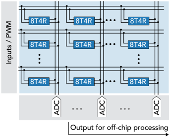
### Visual Description
\n
## Diagram: 8T4R System Architecture
### Overview
The image depicts a block diagram of an 8T4R (likely 8-Transmit, 4-Receive) system architecture. It illustrates the interconnection between input signals (Inputs/PWM) and output signals (Output for off-chip processing) via a matrix of 8T4R blocks and Analog-to-Digital Converters (ADCs). The diagram shows a repetitive structure, indicated by the ellipsis (...), suggesting a larger array of these components.
### Components/Axes
The diagram consists of the following key components:
* **8T4R Blocks:** Rectangular blocks labeled "8T4R". These appear to be the core processing elements.
* **Inputs/PWM:** A gray rectangular area labeled "Inputs / PWM" representing the input signals to the system.
* **ADCs:** Blocks labeled "ADC" representing Analog-to-Digital Converters.
* **Output for off-chip processing:** A label indicating the destination of the processed signals.
* **Interconnecting Lines:** Lines connecting the 8T4R blocks to both the input signals and the ADCs.
There are no explicit axes in this diagram. The arrangement is spatial, representing connections and flow.
### Detailed Analysis or Content Details
The diagram shows a matrix-like arrangement of 8T4R blocks.
* **Input Connections:** Each 8T4R block receives input from the "Inputs / PWM" section. Multiple input lines connect to each 8T4R block, suggesting parallel processing or multiple input channels.
* **8T4R Matrix:** The 8T4R blocks are arranged in rows and columns. The ellipsis (...) indicates that the matrix extends beyond what is visible in the diagram.
* **ADC Connections:** Each column of 8T4R blocks is connected to a single ADC. This suggests that the ADCs are responsible for converting the output of each column into a digital signal.
* **Output:** The output of the ADCs is labeled "Output for off-chip processing," indicating that the digital signals are sent to an external processing unit.
The diagram does not provide specific numerical values or parameters for the 8T4R blocks or ADCs. It is a high-level architectural representation.
### Key Observations
* **Parallel Processing:** The arrangement of 8T4R blocks and ADCs suggests a parallel processing architecture, where multiple input signals are processed simultaneously.
* **Matrix Structure:** The matrix-like arrangement of 8T4R blocks allows for flexible signal routing and processing.
* **Modular Design:** The repetitive structure of the diagram suggests a modular design, where the system can be easily scaled by adding more 8T4R blocks and ADCs.
### Interpretation
This diagram illustrates a system architecture commonly used in wireless communication or signal processing applications. The 8T4R blocks likely perform some form of signal amplification, filtering, or modulation. The ADCs convert the analog output of the 8T4R blocks into digital signals for further processing. The "Output for off-chip processing" suggests that the system is part of a larger system, where the processed signals are sent to an external processor for tasks such as decoding, error correction, or control.
The use of 8 transmit and 4 receive elements suggests a Multiple-Input Multiple-Output (MIMO) system, which is used to improve the capacity and reliability of wireless communication links. The diagram highlights the key components and their interconnections, providing a clear understanding of the system's overall architecture. The ellipsis indicates that the system can be scaled to accommodate a larger number of input and output channels. The diagram does not provide details about the specific functionality of the 8T4R blocks or ADCs, but it provides a valuable overview of the system's overall structure.
</details>
. .
F igure 3 . 8 : Illustration of the working principle of phase-change devices and their integration into a crossbar architecture. a , Phase switching behavior of PCM devices. SET and RESET pulses can be used to transition between the amorphous and the crystalline phase. b , The PCM devices from a can be incorporated into a crossbar array structure. In our work, four PCM devices are used in a differential manner to represent each weight element
Similar to Section 3 . 1 , we tested the network on a 1 D continual pattern regression task, using an RSNN architecture with 100 recurrently connected LIF neurons and one leaky-integrator output unit (Eq. 3 . 1 ) Again, the RSNN is driven by fixed-rate Poisson spikes from 100 input neurons, with a membrane decay time constant of 30 ms for both recurrent and output units.
To optimize resources allocation, we strategically embedded trainable parameters W in , W rec and W out, within Core 1 , and the feedback matrix B out within Core 2 . This architectural design, illustrated in Fig. 3 . 9 , enables network inference on one core and error-based learning signal generation on the other. We use e-prop for computing the approximated gradients for network weights and leverage the mixed-precision algorithm to accumulate gradients in a high-precision unit. This unit also serves to store the dataset, to compute neuron activations and eligibility traces, and to calculate network error.
F igure 3 . 9 : Task illustration and realization of the network on neuromorphic hardware. Realization of the regression task on a neuromorphic hardware using two cores with PCM crossbar arrays. The trainable parameters W in , W rec and W out are placed into Core 1 and B out is placed into Core 2 . The neuromorphic is used to perform the matrix-vector multiplication required to compute the network activity and the learning signal. A high-precision unit is used to track the individual gradients which are applied to the trainable parameters.
<details>
<summary>Image 17 Details</summary>
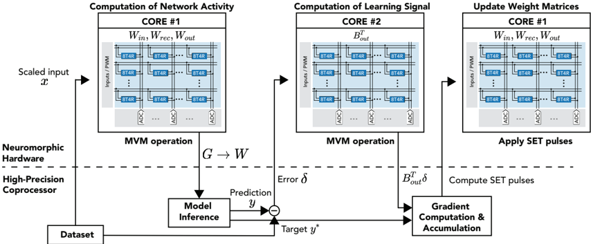
### Visual Description
\n
## Diagram: Neuromorphic Computing Pipeline
### Overview
This diagram illustrates a pipeline for neuromorphic computing, specifically detailing the computation of network activity, learning signal, and weight matrix updates. The process involves three main cores and utilizes neuromorphic hardware and a high-precision coprocessor. The diagram shows the flow of data from a dataset through model inference, error calculation, gradient computation, and finally, weight updates.
### Components/Axes
The diagram is segmented into three main blocks representing the three cores:
1. **Computation of Network Activity (CORE #1):** Inputs/PWM, Win, Wrec, Wout, ADC.
2. **Computation of Learning Signal (CORE #2):** Inputs/PWM, Bout, ADC.
3. **Update Weight Matrices (CORE #1):** Inputs/PWM, Win, Wrec, Wout, ADC.
Additional components include:
* **Scaled Input (x):** The initial input data.
* **Neuromorphic Hardware:** The underlying hardware platform.
* **High-Precision Coprocessor:** Assists in computations.
* **Dataset:** The source of input data.
* **Model Inference:** The process of generating a prediction.
* **Prediction (y):** The output of the model.
* **Target (y*):** The desired output.
* **Error (δ):** The difference between prediction and target.
* **Gradient Computation & Accumulation:** Calculates the gradient of the error.
* **MVM Operation:** Matrix-Vector Multiplication.
* **G → W:** Represents the weight update process.
* **Boutδ:** Represents the learning signal.
### Detailed Analysis or Content Details
The diagram depicts a data flow.
1. **Scaled Input (x):** The process begins with a scaled input 'x' from a 'Dataset'. This input is fed into 'CORE #1' (Computation of Network Activity).
2. **CORE #1:** This core receives 'Inputs/PWM' and utilizes weight matrices 'Win', 'Wrec', and 'Wout'. The core contains multiple 'BT4R' blocks (approximately 8x8 grid) and 'ADC' (Analog-to-Digital Converter) components. The output of this core is fed into 'Model Inference'.
3. **Model Inference:** The 'Model Inference' block generates a 'Prediction' (y).
4. **Error Calculation:** The 'Prediction' (y) is compared to a 'Target' (y*) to calculate an 'Error' (δ).
5. **CORE #2:** The 'Error' (δ) is then fed into 'CORE #2' (Computation of Learning Signal), which also receives 'Inputs/PWM' and utilizes a weight matrix 'Bout'. Similar to CORE #1, it contains 'BT4R' blocks and 'ADC' components. The output of CORE #2 is 'Boutδ'.
6. **Gradient Computation & Accumulation:** 'Boutδ' is used in 'Gradient Computation & Accumulation'.
7. **Weight Update:** The output of 'Gradient Computation & Accumulation' is used to update the weight matrices 'Win', 'Wrec', and 'Wout' in 'CORE #1' (Update Weight Matrices) via the 'G → W' transformation. This core also receives 'Inputs/PWM', 'BT4R' blocks, and 'ADC' components. The update is applied using 'SET pulses'.
8. **MVM Operation:** Both CORE #1 and CORE #2 perform a 'MVM operation'.
The 'BT4R' blocks appear to represent individual processing elements within the cores. The 'ADC' components likely convert analog signals to digital values. The diagram does not provide specific numerical values for the weights or input signals.
### Key Observations
* The diagram highlights a closed-loop system where predictions are compared to targets, and the resulting error is used to update the weights.
* The use of 'SET pulses' suggests a spike-based or event-driven computation paradigm.
* The diagram emphasizes the role of neuromorphic hardware and a high-precision coprocessor in accelerating the computation.
* The repeated use of 'Inputs/PWM' suggests Pulse Width Modulation is used for input representation.
* The cores appear to have a similar structure, with a grid of 'BT4R' blocks and 'ADC' components.
### Interpretation
This diagram illustrates a simplified view of a neuromorphic computing system. The system aims to mimic the biological brain by using spiking neural networks and event-driven computation. The use of neuromorphic hardware and a high-precision coprocessor suggests an attempt to overcome the limitations of traditional von Neumann architectures for machine learning tasks. The pipeline demonstrates how input data is processed, predictions are made, errors are calculated, and weights are updated to improve the model's accuracy. The 'SET pulses' likely represent the mechanism for adjusting the synaptic weights in the neuromorphic hardware. The diagram suggests a focus on energy efficiency and parallel processing, which are key advantages of neuromorphic computing. The diagram does not provide details on the specific neural network architecture or the learning algorithm used. It is a high-level overview of the data flow and key components involved in the process.
</details>
Before transitioning to the hardware testing, a comprehensive investigation of network performance was conducted within a simulation framework, subjecting the network to various hardware constraints. This involved utilizing weights with varying precision levels, including 32 -bit floating point (SW 32 bit), 8 -bit and 4 -bit fixed-point (SW 8 bit and SW 4 bit), and weights based on a PCM model (SW PCM), as depicted in Fig. 3 . 2 .
The results, illustrated in Figure 3 . 10 , were obtained using four distinct random seeds. Notably, the performance metrics using 32 -bit and 8 -bit precision were comparable, affirming the robustness of the network under reduced precision. The network's performance remained resilient even with 4 -bit ( E = 3.93 ± 0.58 ) or simulated PCM ( E = 3.72 ± 0.53 ). Although a slight degradation was observed with hardware ( E = 5.59 ± 1.29 ), the network succeded in reproducing the target pattern (Fig. 3 . 10 b). The individual subpanels within this figure effectively visualize the patterns at different stages of training: the beginning, after 30 iterations, and at the end of training.
The histograms in Fig. 3 . 10 c show the distributions of trainable matrices before and after training. Notably, modifications in the output weights were instrumental in achieving accurate pattern generation. The average firing rate was maintained at approximately 10 Hz through regularization. This ensured sparsity in both communication and programming pulses, crucial for energy efficiency and extending device longevity. The sparse application of SET pulses, evident in Figure 3 . 10 d, further underscores this efficiency. Specifically, only 2 -3 pulses per iteration were required for the output weight matrix, even though it comprised 100 elements. This highlights the effectiveness of the gradient accumulation in reducing the number of programming pulses and, consequently, the overall energy consumption.
## 3 . 2 . 2 Discussion
We have demonstrated that training RSNNs with the e-prop local weight update rule, using a hardware-in-the-loop approach, can be robust to both limited computational precision and analog imperfections inherent to memristive devices. Furthermore, our experiments show that this system achieves performance competitive with conventional software implementations with full-precision. The RSNN neurons exhibited a low firing rate, and mixed-precision training significantly reduced the number of PCM programming pulses. This reduction in programming activity not only enhances energy efficiency but also mitigates potential endurance issues associated with frequent
device switching. Our findings enable RSNNs trained with biologically-inspired algorithms to be deployed on memristive neuromorphic hardware for sparse and online learning.
In the following Section 3 . 3 , we will present how eligibility traces can be implemented with volatile memristive devices, enabling more scalable credit assignment on neuromorphic hardware.
F igure 3 . 10 : Results of our training approach realized with different synapse models. a , Evolution of the squared error using different synapse models, averaged over 4 random initializations. b , Visual comparison of the network output and the target pattern, at the beginning of training (first subpanel), after 30 training iterations (second subpanel) and after training (third subpanel). c , Histogram of the trainable weight matrices before and after training. d , Number of SET pulses applied to the individual weight matrices.
<details>
<summary>Image 18 Details</summary>
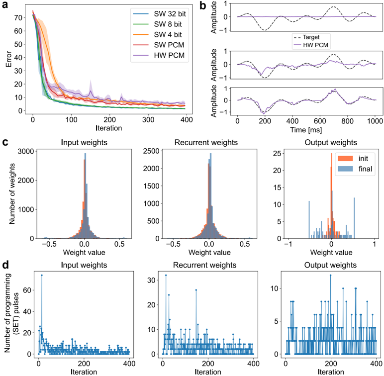
### Visual Description
## Chart Compilation: Training Error and Weight Distribution
### Overview
The image presents a compilation of four charts (a, b, c, and d) illustrating the training process and weight distribution of a neural network, likely a recurrent neural network, using different precision levels (32-bit, 8-bit, 4-bit, PCM) and hardware (HW) vs. software (SW) implementations. Chart 'a' shows the error reduction during training iterations. Chart 'b' displays the amplitude of the output signal over time for the HW PCM implementation compared to a target signal. Charts 'c' and 'd' visualize the distribution of input, recurrent, and output weights, both initially and after training, and the number of programming pulses used during training, respectively.
### Components/Axes
* **Chart a:**
* X-axis: Iteration (0 to 400)
* Y-axis: Error (0 to 60)
* Legend:
* SW 32 bit (Blue)
* SW 8 bit (Green)
* SW 4 bit (Red)
* SW PCM (Orange)
* HW PCM (Teal)
* **Chart b:**
* X-axis: Time [ms] (0 to 1000)
* Y-axis: Amplitude (approximately -1.5 to 1.5)
* Legend:
* Target (Black dashed line)
* HW PCM (Teal)
* **Chart c:**
* X-axis: Weight value (approximately -0.5 to 0.5 for Input/Recurrent, -1 to 1 for Output)
* Y-axis: Number of weights (0 to 3000 for Input/Recurrent, 0 to 15 for Output)
* Sub-charts: Input weights, Recurrent weights, Output weights
* Legend:
* init (Orange)
* final (Blue)
* **Chart d:**
* X-axis: Iteration (0 to 400)
* Y-axis: Number of programming (SET) pulses (0 to 50)
* Sub-charts: Input weights, Recurrent weights, Output weights
* Legend: None (Data represented by bars)
### Detailed Analysis or Content Details
**Chart a: Error vs. Iteration**
* The SW 32 bit line (blue) shows the fastest initial error reduction, reaching approximately 5 error units by iteration 100 and leveling off around 2-3 error units.
* The SW 8 bit line (green) initially decreases slower than SW 32 bit, but converges to a similar final error level (around 3-4 error units) by iteration 400.
* The SW 4 bit line (red) exhibits the slowest initial decrease and reaches a higher final error level (around 8-10 error units) compared to the 32-bit and 8-bit versions.
* The SW PCM line (orange) shows a moderate decrease, converging to approximately 5-6 error units.
* The HW PCM line (teal) demonstrates a rapid initial decrease, similar to SW 32 bit, and reaches a very low final error level (around 1-2 error units).
**Chart b: Amplitude vs. Time**
* The Target signal (black dashed line) is a periodic waveform with amplitude oscillating between approximately -1 and 1.
* The HW PCM signal (teal) closely tracks the Target signal, exhibiting a similar waveform and amplitude. There is a slight phase shift.
**Chart c: Weight Distribution**
* **Input Weights:** The initial distribution (orange) is relatively uniform. The final distribution (blue) is bimodal, with peaks around -0.2 and 0.2.
* **Recurrent Weights:** The initial distribution (orange) is approximately normal, centered around 0. The final distribution (blue) is also approximately normal, but shifted slightly towards 0 and with a narrower spread.
* **Output Weights:** The initial distribution (orange) is relatively uniform. The final distribution (blue) is bimodal, with peaks around -1 and 1.
**Chart d: Programming Pulses vs. Iteration**
* **Input Weights:** The number of programming pulses fluctuates around an average of approximately 10-15 pulses, with some spikes early in training.
* **Recurrent Weights:** The number of programming pulses shows a significant peak around iteration 50-100, reaching up to 25 pulses, and then decreases to a stable level of around 5-10 pulses.
* **Output Weights:** The number of programming pulses exhibits multiple peaks throughout training, reaching up to 10-15 pulses, and then stabilizes around 5-8 pulses.
### Key Observations
* HW PCM achieves the lowest training error, suggesting superior performance compared to software implementations.
* Lower precision (4-bit) results in higher training error, indicating a trade-off between precision and performance.
* Weight distributions change significantly during training, indicating that the network is learning.
* The number of programming pulses varies during training, suggesting that different weights require different levels of adjustment.
* Recurrent weights require a burst of programming pulses early in training.
### Interpretation
The data suggests that a hardware implementation of PCM with high precision (32-bit or 8-bit) is optimal for training this recurrent neural network. The error curves (Chart a) clearly demonstrate that HW PCM converges to the lowest error, while lower precision software implementations struggle to achieve the same level of accuracy. The weight distributions (Chart c) show that the network is learning to adjust its weights to minimize the error. The programming pulse data (Chart d) provides insights into the learning process, revealing that different weight groups require different levels of adjustment during training. The close tracking of the target signal by the HW PCM implementation (Chart b) confirms its ability to accurately represent the desired output. The bimodal weight distributions in the input and output layers suggest that the network is learning to represent distinct features or categories. The initial spike in programming pulses for recurrent weights may indicate a period of rapid adaptation to the temporal dynamics of the input data. Overall, the data highlights the importance of both hardware and precision in achieving optimal performance in neural network training.
</details>
## 3 . 3 scalable synaptic eligibility traces with volatile memristive devices
Dedicated hardware implementations of spiking neural networks that combine the advantages of mixed-signal neuromorphic circuits with those of emerging memory technologies have the potential of enabling ultra-low power pervasive sensory processing. To endow these systems with additional flexibility and the ability to learn to solve specific tasks, it is important to develop appropriate on-chip learning mechanisms. Recently, a new class of three-factor spike-based learning rules have been proposed that can solve the temporal credit assignment problem and approximate the error back-propagation algorithm on complex tasks. However, the efficient implementation of these rules on hybrid CMOS/memristive architectures is still an open challenge. Here we present a new neuromorphic building block, called PCM-trace, which exploits the drift behavior of phase-change materials to implement long-lasting eligibility traces, a critical ingredient of threefactor learning rules. We demonstrate how the proposed approach improves the area efficiency by > 10 × compared to existing solutions and demonstrates a technologically plausible learning algorithm supported by experimental data from device measurements.
## 3 . 3 . 1 Introduction
Neuromorphic engineering uses electronic analog circuit elements to implement compact and energy-efficient intelligent cognitive systems [ 187 -190 ]. Leveraging substrate's physics to emulate biophysical dynamics is a strong incentive toward ultra-low power and real-time implementations of neural networks using mixed-signal memristive event-based neuromorphic circuits [ 144 , 191 -193 ]. The majority of these systems are currently deployed in edge-computing applications only in inference mode , in which the network parameters are fixed. However, learning in edge computing can have many advantages, as it enables adaptation to changing input statistics, sensory degradations, reduced network congestion, and increased privacy. Indeed, there have been multiple efforts implementing Spike-Timing Dependent Plasticity (STDP)-variants and Hebbian learning using neuromorphic processors [ 168 , 181 , 194 ]. These methods control LongTerm Depression (LTD) or Long-Term Potentiation (LTP) by specific local features of pre- and post-synaptic activities. However, local learning rules themselves do not provide any guarantee that network performance will improve in multi-layer or recurrent networks. Local error-driven approaches, e.g., the Delta Rule, aim to solve this problem but fail to assign credit for neurons that are multiple synapses away from the network output [ 195 , 196 ]. On the other hand, it has been recently shown that by using external third-factor neuromodulatory signals (e.g., reward or prediction error in reinforcement learning, teaching signal in supervised learning), this can be achieved in hierarchical networks [ 197 , 198 ]. However, there needs to be a mechanism for synapses to remember their past activities for long periods of time, until the reward event or teacher signal is presented. In the brain, these signals are believed to be implemented by calcium ions, or CAMKII enzymes in the synaptic spine [ 199 ] and are called eligibility traces. In machine learning, algorithmic top-down analysis of the gradient descent demonstrated how local eligibility traces at synapses allow networks to reach performances comparable to error back-propagation algorithm on complex tasks [ 75 , 85 , 200 ].
There are already neuromorphic platforms that support the synaptic eligibility trace implementation such as Loihi [ 89 ], BrainScales [ 90 ] or SpiNNaker [ 91 ]. The learning (weight update) in these platforms is only supported through the use of digital processors, hence the numerical trace calculation leads to extremely memory intensive operations forming a von Neumann bottleneck [ 92 , 93 ]. Especially when the eligibility trace calculation is per synapse (instead of per neuron) the memory overhead quickly becomes overwhelming as the number of traces scales quadratically with the number of neurons in the network. And unlike the convolutional architectures on digital neuromorphic processors, where weight sharing reduces the memory bandwidth, the eligibility traces cannot be shared due to their activity dependent nature.
On the other hand, mixed-signal neuromorphic processors that perform in-memory computation can emulate the desired neural and synaptic dynamics using the physics of the analog substrate [ 201 , 202 ]. Differential-Pair Integrator (DPI) based circuits [ 202 , 203 ] which rely on
T able 3 . 3 : Eligibility Traces in Gradient-Estimating Learning Rules
| Learning rule | Pre-synaptic terms | Post-synaptic terms |
|----------------------------|----------------------|-----------------------|
| e-prop (LIF) [ 82 ] | x j | - |
| e-prop (ALIF) [ 82 ] | x j | ψ i |
| Sparse RTRL [ 83 ] | x j | - |
| BDSP [ 39 ] | x j | - |
| SuperSpike [ 85 ] | ϵ ∗ x j | ψ i |
| Sparse Spiking G.D. [ 86 ] | x j | - |
accumulating volatile information on capacitors, in principle can be used to implement eligibility traces. Recently, a substantial progress has been made [ 94 ] in implementing slow-dynamics DPI synapse circuits using advanced Fully Depleted Silicon-On-Insulator (FDSOI) technologies. By combining reverse body biasing and self-cascoding techniques [ 204 ], these circuits can achieve ∼ 6 s long synaptic traces [ 94 ]. However, resulting area due to large capacitor sizes and areadependent leakage due to Alternate Polarity Metal On Metal (APMOM) structures hinder the scalability of such hardware implementations.
In this work, we present a novel approach to exploit the drift behavior of PCM devices to intrinsically perform eligibility trace computation over behavioral timescales. We present the PCM-trace building block as a hybrid memristive-CMOS circuit solution that can lead to recordlow area requirements per synapse. To the best of our knowledge, this is the first work that uses a memristive device not only to store the weight of synapses, but also to keep track of synaptic eligibility to interact with a third factor toward scalable next-generation on-chip learning.
## Eligibility traces in machine learning and neuroscience
Eligibility trace is a decaying synaptic state variable that tracks recency and frequency of synaptic events, as described in Eq. ( 3 . 5 ). The trace state, e ij , of the synapse between pre-synaptic neuron j and post-synaptic neuron i is controlled by usually a linear function of pre-synaptic spiking activity f j ( xj ) and non-linear function of the post-synaptic activity gi ( xi ) , such that
$$\frac { d e _ { i j } } { d t } = - \tau _ { e } e + \eta f _ { j } \left ( x _ { j } \right ) g _ { i } \left ( x _ { i } \right ) & & ( 3 . 5 )$$
, where τ e is the time-constant of the trace and η is the constant scaling factor [ 197 ].
The function of eligibility trace is to keep the temporal correlation history of f j ( xj ) and gi ( xi ) available in the synapse, by accumulating instantaneous correlation events, called synaptic tags . From the top-down gradient-based machine learning perspective, various learning rules require eligibility trace functionality as a part of the network architecture and specifies their own synaptic tag requirements, f j · gi , (i.e., what information to accumulate on the synapse).
Table 3 . 3 summarizes some of the recently developed biologically-plausible, local learning rules employing eligibility traces within the supervised learning framework. Most of the listed learning rules accumulate pre-synaptic events, xj , seldom further smoothed with ϵ (causal membrane kernel), whereas some learning rules additionally require the information of a surrogate partial derivative function of post-synaptic state, ψ i . By approximating the gradient-based optimization for spiking neural networks, these learning rules support competitive performance on standard audio and image classification datasets such as TIMIT Dataset [ 205 ], Spiking Heidelberg Digits [ 206 ], Fashion-MNIST [ 207 ], Neuromorphic-MNIST [ 208 ], CIFAR10 [ 209 ] and even ImageNet [ 210 ].
In the RL, the advantages of having long-lasting synaptic eligibility traces are more evident. Eligibility traces carry the temporal synaptic tag information into the future, allowing backward view when the sparse reward arrives from the environment [ 211 ]. By doing so, eligibility traces assist solving the distal reward problem [ 88 ] (how the brain assigns credits/blame for neurons if
the activity patterns responsible for the reward are no longer exist when the reward arrives) by bridging the milli-second neuronal timescales and second-long behavioral timescales. Almost any Temporal Difference (TD) method e.g., Q-learning or SARSA can benefit from eligibility traces to learn more efficiently [ 211 ]. The policy gradient methods utilizing the temporal discounting operation e.g., discounted reward [ 211 ] or discounted advantage [ 212 ], naturally demands the synaptic eligibility traces. Moreover, some on-policy and off-policy RL models can explain behavioral and physiological experiments on multiple sensory modalities, only if they are equipped with synaptic eligibility traces with > 10 s decay time [ 213 ].
Eligibility traces are also deeply rooted in neurobiology. The synaptic machinery that implements the eligibility trace might be calcium-based mechanisms in the spine e.g., CamKII [ 214 , 215 ], or metastable transient state of molecular dynamics inside the synapse [ 216 ]. In the visual and frontal cortex, in-vivo STDP experiments suggest that pre-before-post pairings induces a synaptic tagging that decays over ∼ 10 s and result in LTP with the arrival of the third-factor neuromodulator noradrenaline [ 217 ]. In the hippocampus, Brzosko, Schultz & Paulsen [ 218 ] found that post-before-pre pairings can result in LTP if the third-factor neuromodulator dopamine arrives in the range of minutes.
In summary, both top-down approaches following machine learning principles and bottom-up approaches built upon in-vivo and in-vitro synaptic plasticity experiments imply the importance of having eligibility traces in neural architectures.
## 3 . 3 . 2 PCM-trace: Implementing eligibility traces with PCM drift
## 3 . 3 . 2 . 1 PCM Measurements
Temporal evolution of electrical resistivity is a widely-observed phenomenon in PCM due to the rearrangements of atoms in the amorphous phase [ 219 ]. This behavior is commonly referred to as structural relaxation or drift. To start the drift, a strong RESET pulse is applied to induce a crystalline to amorphous phase transition where the PCM is melted and quenched. The lowordered and highly-stressed amorphous state then evolves to a more energetically favorable glass state within tens of seconds [ 112 ].
At constant ambient temperature, the resistivity follows
$$R ( t ) = R ( t _ { 0 } ) \left ( \frac { t } { t _ { 0 } } \right ) ^ { \nu } , \quad \, \begin{array} { l } { { ( 3 . 6 ) } } \end{array}$$
where R ( t 0 ) is the resistance measured at time t 0 and ν is the drift coefficient. It has been experimentally verified by many groups that Eq. ( 3 . 6 ) can successfully capture the drift dynamics [ 112 , 156 , 220 ], from microseconds to hours range [ 221 ].
F igure 3 . 11 : Experimental (dots), and simulated (dashed lines) resistance drift characteristics at constant room temperature.
<details>
<summary>Image 19 Details</summary>
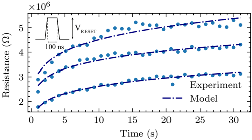
### Visual Description
\n
## Chart: Resistance vs. Time
### Overview
The image presents a chart illustrating the relationship between resistance (in Ohms, Ω) and time (in seconds, s). Two data series are displayed: experimental data represented by solid blue circles, and a model prediction represented by dashed blue lines. A small inset diagram in the top-left corner depicts a pulse waveform with a labeled reset voltage (V<sub>RESET</sub>) and pulse duration (100 ns).
### Components/Axes
* **X-axis:** Time (s), ranging from 0 to 30 seconds.
* **Y-axis:** Resistance (Ω), ranging from approximately 1.5 x 10<sup>6</sup> to 5.5 x 10<sup>6</sup> Ohms. The scale is explicitly shown as "x 10<sup>6</sup>".
* **Data Series 1:** "Experiment" - Represented by solid blue circles.
* **Data Series 2:** "Model" - Represented by dashed blue lines.
* **Legend:** Located in the bottom-right corner, labeling the two data series.
* **Inset Diagram:** A pulse waveform in the top-left corner, labeled with "V<sub>RESET</sub>" and "100 ns".
### Detailed Analysis
The chart displays the change in resistance over time for both the experimental data and the model.
**Experiment Data (Solid Blue Circles):**
The experimental data shows an increasing resistance over time.
* At t = 0 s, Resistance ≈ 1.8 x 10<sup>6</sup> Ω.
* At t = 5 s, Resistance ≈ 3.2 x 10<sup>6</sup> Ω.
* At t = 10 s, Resistance ≈ 4.2 x 10<sup>6</sup> Ω.
* At t = 15 s, Resistance ≈ 4.6 x 10<sup>6</sup> Ω.
* At t = 20 s, Resistance ≈ 4.8 x 10<sup>6</sup> Ω.
* At t = 25 s, Resistance ≈ 4.9 x 10<sup>6</sup> Ω.
* At t = 30 s, Resistance ≈ 5.1 x 10<sup>6</sup> Ω.
**Model Data (Dashed Blue Lines):**
The model data also shows an increasing resistance over time, but with a steeper initial increase and a slower rate of increase as time progresses. There are three dashed lines, representing three different model predictions.
* **Top Model Line:**
* At t = 0 s, Resistance ≈ 2.2 x 10<sup>6</sup> Ω.
* At t = 5 s, Resistance ≈ 3.8 x 10<sup>6</sup> Ω.
* At t = 10 s, Resistance ≈ 4.7 x 10<sup>6</sup> Ω.
* At t = 15 s, Resistance ≈ 5.0 x 10<sup>6</sup> Ω.
* At t = 20 s, Resistance ≈ 5.2 x 10<sup>6</sup> Ω.
* At t = 25 s, Resistance ≈ 5.3 x 10<sup>6</sup> Ω.
* At t = 30 s, Resistance ≈ 5.4 x 10<sup>6</sup> Ω.
* **Middle Model Line:**
* At t = 0 s, Resistance ≈ 2.0 x 10<sup>6</sup> Ω.
* At t = 5 s, Resistance ≈ 3.5 x 10<sup>6</sup> Ω.
* At t = 10 s, Resistance ≈ 4.4 x 10<sup>6</sup> Ω.
* At t = 15 s, Resistance ≈ 4.7 x 10<sup>6</sup> Ω.
* At t = 20 s, Resistance ≈ 4.9 x 10<sup>6</sup> Ω.
* At t = 25 s, Resistance ≈ 5.0 x 10<sup>6</sup> Ω.
* At t = 30 s, Resistance ≈ 5.1 x 10<sup>6</sup> Ω.
* **Bottom Model Line:**
* At t = 0 s, Resistance ≈ 1.8 x 10<sup>6</sup> Ω.
* At t = 5 s, Resistance ≈ 3.2 x 10<sup>6</sup> Ω.
* At t = 10 s, Resistance ≈ 4.1 x 10<sup>6</sup> Ω.
* At t = 15 s, Resistance ≈ 4.4 x 10<sup>6</sup> Ω.
* At t = 20 s, Resistance ≈ 4.6 x 10<sup>6</sup> Ω.
* At t = 25 s, Resistance ≈ 4.7 x 10<sup>6</sup> Ω.
* At t = 30 s, Resistance ≈ 4.8 x 10<sup>6</sup> Ω.
**Inset Diagram:**
The inset diagram shows a rectangular pulse with a sharp rise and fall time. The pulse duration is labeled as "100 ns". The reset voltage is labeled as "V<sub>RESET</sub>".
### Key Observations
* The experimental data and the model data both show an increasing resistance over time, indicating a change in the material's properties.
* The model predictions diverge, suggesting different parameter settings or assumptions within the model.
* The experimental data generally falls between the lower and middle model predictions.
* The initial rate of resistance increase is higher for the model predictions than for the experimental data.
### Interpretation
The chart demonstrates the relationship between time and resistance, likely in a material undergoing a change in state (e.g., a phase change memory). The model attempts to predict the experimental behavior, and the comparison reveals the model's accuracy and limitations. The inset diagram suggests that a reset pulse (V<sub>RESET</sub>) is applied to the material, potentially triggering the observed resistance change. The divergence in model predictions indicates sensitivity to model parameters. The fact that the experimental data falls between the model predictions suggests that the model is reasonably accurate, but may require further refinement to capture the nuances of the experimental behavior. The slower initial increase in experimental resistance compared to the model could indicate a delay in the material's response to the reset pulse or a difference in the material's properties compared to the model's assumptions.
</details>
With the collaboration of CEA-LETI, we integrated Ge 2 Sb 2 Te 5 -based PCM in state-of-the-art PCM heater-based devices fabricated in the Back-End-Of-Line (BEOL) based on 130 nm CMOS technology. The PCM thickness is 50 nm with the bottom size of 3600 nm 2 . Drift measurements
F igure 3 . 12 : Accumulating eligibility trace using PCM-trace drift model (Eq. 3 . 7 ). After resetting the PCM-trace device at t = 0, 5 random synaptic tags are applied to the synapse, implemented by a gradual SET for each tag that results in 50% increase in the conductivity. The device can keep the eligibility trace for more than 10 s.
<details>
<summary>Image 20 Details</summary>
### Visual Description
\n
## Line Chart: Conductance Over Time
### Overview
The image presents a line chart illustrating the change in conductance (µS) over time (seconds). Two distinct lines represent "Accumulating e-trace" and "Synaptic tagging". A shaded region labeled "Higher Baseline" is present in the background. The chart focuses on the initial 12 seconds of observation.
### Components/Axes
* **X-axis:** Time (s), ranging from 0 to 12 seconds.
* **Y-axis:** Conductance (µS), ranging from approximately 0 to 1.1 µS.
* **Lines:**
* "Accumulating e-trace" - Solid black line.
* "Synaptic tagging" - Dotted black line.
* **Shaded Region:** "Higher Baseline" - Light blue shaded area covering the majority of the chart area from approximately 2 seconds onwards.
* **Legend:** Located in the bottom-left corner, identifying the lines.
### Detailed Analysis
* **Accumulating e-trace:** This line begins at approximately 0.6 µS at time 0 seconds. It rapidly increases to a peak of approximately 1.0 µS around 0.7 seconds. Following the peak, the line exhibits a steep decline, leveling off to approximately 0.55 µS by 12 seconds. The trend is initially sharply upward, followed by a gradual decay.
* **Synaptic tagging:** This line starts at approximately 0.6 µS at time 0 seconds. It shows a rapid initial increase, peaking at approximately 1.1 µS around 0.6 seconds. The line then rapidly decreases, crossing below 0.5 µS by approximately 2 seconds, and continues to decline, reaching approximately 0.4 µS by 12 seconds. The trend is a sharp initial rise followed by a more rapid decay than the "Accumulating e-trace".
* **Higher Baseline:** The shaded region indicates a higher baseline conductance level, starting around 2 seconds and continuing to 12 seconds. The exact conductance value within this region is not explicitly defined but is visually represented as being above the level of the "Accumulating e-trace" line at 12 seconds.
### Key Observations
* Both conductance traces exhibit a rapid initial increase followed by a decay.
* The "Synaptic tagging" trace has a higher peak conductance and a faster decay rate compared to the "Accumulating e-trace" trace.
* The "Higher Baseline" region suggests a sustained elevated conductance level after the initial transient events.
* The initial rapid increase and subsequent decay of both traces occur within the first 2 seconds.
### Interpretation
The chart likely represents the dynamics of conductance changes in a biological system, potentially related to synaptic plasticity. The "Accumulating e-trace" could represent a cumulative effect of electrical signals, while "Synaptic tagging" might represent a more transient process involved in marking synapses for long-term potentiation or depression. The "Higher Baseline" suggests a sustained change in the system's overall conductance, possibly due to the activation of other pathways or mechanisms. The difference in decay rates between the two traces suggests that the underlying processes have different time scales. The initial rapid increase and decay could represent the initial response to a stimulus, while the subsequent sustained conductance level reflects a longer-lasting effect. The data suggests that synaptic tagging is a faster, more transient process than accumulating e-trace. The higher baseline could indicate a shift in the system's overall excitability.
</details>
were performed on three devices to monitor the temporal evolution of the resistance in the HRS state, particularly confirming the model in Eq. ( 3 . 6 ). The test was conducted by first resetting all the cells by applying a RESET pulse to the heater, which has a width of 100 ns with 5 ns rising and falling times, and a peak voltage of 1.85 V. Then, an additional programming pulse is used to bring the devices to different initial conditions, corresponding to R ( t = 1 s ) = [ 1.77 M Ω , 2.39 M Ω , 2.89 M Ω ] . The low-field device resistances are measured every 1 s for 30 s by applying a READ pulse which has the same timing of the RESET pulse but a peak voltage of 0.05 V.
PCM-trace is a novel method to implement seconds-long eligibility trace for the synapse using the drift feature of PCM. By writing Eq. ( 3 . 6 ) as a difference equation of the conductance, we can show that the temporal evolution of the conductance has decay characteristics similar to Eq. ( 3 . 5 ) such that G t + ∆ t ij = ( t -t p t -t p + ∆ t ) ν G t ij , where G t 0 ij = 1/ R t 0 ij , and t p is the last programming time as drift re-initializes with every gradual SET [ 81 , 222 ]. The main difference is that the rate of change in PCM resistivity is a function of time; nevertheless, its time constant is comparable for behavioral time-scales as τ PCM = -∆ t / log (( t / ( t + ∆ t )) ν ) is on the order of tens of seconds [ 213 ]. Therefore, the PCM-trace dynamics can emulate the eligibility trace of the synapse as follows:
$$G _ { i j } ^ { t + \Delta t } = \left ( \frac { t - t _ { p } } { t - t _ { p } + \Delta t } \right ) ^ { \nu } G _ { i j } ^ { t } + \eta f _ { j } ( x _ { j } ^ { t } ) g _ { i } ( x _ { i } ^ { t } )$$
In the PCM-trace method (Eq. 3 . 7 ), the accumulating term on the eligibility trace is implemented by applying a gradual SET to the PCM device whenever the synapse is tagged. To maximize the number of accumulations a PCM device can handle without getting stuck in the LRS regime, some operational conditions need to be satisfied. We initialize the device to HRS by applying a strong RESET pulse, and wait for an initialization time t init of at least 250 ms for the device resistance to increase. If t init is too short, the device conductance would still be too high to be able to accumulate enough tags; and if it is too long, the decay will be weaker (see Eq. 3 . 6 ). Initialization time can be modulated to reach the desired drift speed depending on the material choice and the application. After the initialization time, whenever the synapse is tagged, a single gradual SET (with an amplitude of 100 µA and a pulse width of 100 ns with 5 ns rising and falling times) is applied. To make sure that the device stays in the HRS, a read-verify-set scheme can be used. Finally, the value of the eligibility trace can be measured after seconds by reading the conductance of the device (see Fig. 3 . 12 ).
## 3 . 3 . 3 Multi PCM-trace: Increasing the dynamic range of traces
The number of gradual SET pulses applied to a single PCM-trace device is limited, because each pulse partially increases the device conductivity and eventually move the device toward its LRS ( < 2 M Ω ), where the drift converges to a higher baseline level. This problem can be solved by storing the synaptic eligibility trace distributed across multiple PCM devices, as in Fig. 3 . 13 .
F igure 3 . 13 : Multi PCM-trace concept. Each synapse has a weight and a PCM-trace block where multiple parallel PCM devices keep the eligibility trace of the synapse with their natural drift behavior.
<details>
<summary>Image 21 Details</summary>
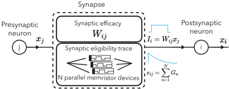
### Visual Description
\n
## Diagram: Synapse Model
### Overview
The image depicts a diagram of a synapse, illustrating the flow of information from a presynaptic neuron to a postsynaptic neuron. The synapse is represented as a processing unit containing synaptic efficacy and synaptic eligibility trace components, with the latter implemented using N parallel memristor devices. The diagram also includes equations representing the signal transmission and eligibility trace calculation.
### Components/Axes
The diagram consists of the following components:
* **Presynaptic Neuron:** Labeled "Presynaptic neuron" and represented by a circle with the input signal "x<sub>j</sub>".
* **Synapse:** Enclosed in a dashed box, labeled "Synapse".
* **Synaptic Efficacy:** A rectangular box within the synapse, labeled "Synaptic efficacy" and containing the variable "W<sub>ij</sub>".
* **Synaptic Eligibility Trace:** A rectangular box within the synapse, labeled "Synaptic eligibility trace" and containing a representation of N parallel memristor devices.
* **N parallel memristor devices:** Represented as a series of four rectangular blocks with pulse-like waveforms within them, labeled "N parallel memristor devices".
* **Postsynaptic Neuron:** Labeled "Postsynaptic neuron" and represented by a circle with the output signal "x<sub>i</sub>".
* **Signal Transmission Equation:** "I<sub>i</sub> = W<sub>ij</sub>x<sub>j</sub>" representing the signal transmission from the presynaptic to the postsynaptic neuron.
* **Eligibility Trace Equation:** "ε<sub>ij</sub> = ∑<sub>n=1</sub><sup>N</sup> G<sub>n</sub>" representing the calculation of the synaptic eligibility trace based on the memristor devices.
### Detailed Analysis or Content Details
The diagram illustrates the following flow:
1. A signal "x<sub>j</sub>" is transmitted from the presynaptic neuron (j) to the synapse.
2. Within the synapse, the signal is multiplied by the synaptic efficacy "W<sub>ij</sub>", resulting in the signal "I<sub>i</sub>" which is transmitted to the postsynaptic neuron (i).
3. The synaptic eligibility trace is calculated based on the output of N parallel memristor devices, represented by the summation equation "ε<sub>ij</sub> = ∑<sub>n=1</sub><sup>N</sup> G<sub>n</sub>".
4. The output of the synaptic eligibility trace influences the synaptic efficacy "W<sub>ij</sub>" (although the feedback loop is not explicitly shown).
The waveforms within the "N parallel memristor devices" block suggest a pulsed or time-varying signal. The equation for the synaptic eligibility trace indicates that the trace is a sum of contributions from each of the N memristor devices (G<sub>n</sub>).
### Key Observations
The diagram highlights the role of memristor devices in implementing the synaptic eligibility trace, which is a crucial component in synaptic plasticity models. The use of N parallel devices suggests a potential for increased computational capacity or robustness. The diagram focuses on the signal flow and mathematical representation of the synapse, rather than the physical structure of the synapse.
### Interpretation
This diagram represents a computational model of a synapse, likely used in the context of artificial neural networks or neuromorphic computing. The use of memristors as the core element of the synaptic eligibility trace suggests an attempt to mimic the biological mechanisms of synaptic plasticity. The equations provided formalize the relationship between the input signal, synaptic efficacy, and eligibility trace. The diagram suggests that the synaptic strength (W<sub>ij</sub>) is modulated by the activity of the presynaptic neuron (x<sub>j</sub>) and the state of the memristor devices (G<sub>n</sub>). The parallel architecture of the memristor devices could enable efficient and scalable implementation of synaptic plasticity. The diagram is a simplified representation of a complex biological system, focusing on the key computational elements and their interactions.
</details>
By successively routing the tags to multiple PCM devices, the number of gradual SET pulses to be applied per single device is significantly reduced. The postsynaptic neuron receives the sum of product of the pre-synaptic activity and the weight block. In parallel, the PCM-trace block calculates the eligibility trace as a function of pre- and post-synaptic activities (Eq. 3 . 7 ), to be used in the weight update. Fig. 3 . 14 demonstrates the increase of effective dynamic range (number of updates to eligibility trace without getting stuck in the LRS) using multiple PCM devices.
F igure 3 . 14 : Accumulating eligibility trace using multi-PCM configuration. Synapse receives 15 tags between 300 ms to 1300 ms which are routed to three different devices shown in the top three plots. The effective eligibility trace is calculated by applying a READ pulse to the parallel PCM devices. The initialization duration and synaptic activity period are shown with dashed lines in the bottom plot. The synaptic efficacy Wij is modified depending on the state of eligibility trace once the third-factor signal arrives.
<details>
<summary>Image 22 Details</summary>
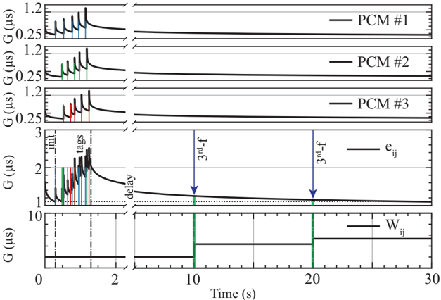
### Visual Description
\n
## Chart: PCM Response Over Time
### Overview
The image presents a time-domain plot showing the response of three Phase Change Memory (PCM) devices (PCM #1, PCM #2, PCM #3) and a combined signal (e<sub>ij</sub>) alongside a write pulse (W<sub>ij</sub>). The plot displays the change in 'G' (likely conductance or a related property) in microseconds (µs) over time in seconds (s). The chart aims to illustrate the dynamic behavior of PCM devices during read and write operations.
### Components/Axes
* **X-axis:** Time (s), ranging from 0 to 30 seconds.
* **Y-axis:** G (µs), with varying scales for each subplot.
* PCM #1, PCM #2, PCM #3: Scale from 0 to 1.2E+6 µs (1.2 million µs).
* e<sub>ij</sub>: Scale from 0 to 3 µs.
* W<sub>ij</sub>: Scale from 0 to 10 µs.
* **Data Series:**
* PCM #1 (Black line)
* PCM #2 (Green line)
* PCM #3 (Red line)
* e<sub>ij</sub> (Black line)
* W<sub>ij</sub> (Green line)
* **Annotations:**
* "init." (initialization)
* "tags"
* "delay"
* "3rd-f" (appears twice, indicating a third frequency component or a related event)
* **Legend:** Located on the right side of the chart, labeling each data series with its corresponding color.
### Detailed Analysis
The chart consists of five subplots stacked vertically.
* **PCM #1:** The black line shows an initial rapid decrease in G, followed by a slow decay towards a stable value around 0.25 µs. The initial drop occurs within approximately 0.5 seconds.
* **PCM #2:** The green line exhibits a similar initial drop in G, but with a more pronounced oscillation before settling around 0.25 µs. The initial drop occurs within approximately 0.5 seconds.
* **PCM #3:** The red line shows a similar initial drop in G, but with a more pronounced oscillation before settling around 0.25 µs. The initial drop occurs within approximately 0.5 seconds.
* **e<sub>ij</sub>:** The black line shows a complex response. Initially, all three PCM responses (black, green, and red) overlap. After approximately 2 seconds, the signal decays, with a noticeable "delay" indicated by an arrow. Around 10 seconds and 20 seconds, there are spikes labeled "3rd-f". The signal stabilizes around 1 µs.
* **W<sub>ij</sub>:** The green line represents a write pulse, consisting of rectangular pulses with a duration of approximately 2 seconds, repeated at intervals of approximately 8 seconds. The amplitude of the pulse is around 10 µs.
**Approximate Data Points (from visual inspection):**
* **PCM #1:** At t=0s, G ≈ 1.2 µs. At t=0.5s, G ≈ 0.3 µs. At t=30s, G ≈ 0.25 µs.
* **PCM #2:** At t=0s, G ≈ 1.2 µs. At t=0.5s, G ≈ 0.3 µs. At t=30s, G ≈ 0.25 µs.
* **PCM #3:** At t=0s, G ≈ 1.2 µs. At t=0.5s, G ≈ 0.3 µs. At t=30s, G ≈ 0.25 µs.
* **e<sub>ij</sub>:** At t=0s, G ≈ 2 µs. At t=2s, G ≈ 1.2 µs. At t=10s, G ≈ 1.1 µs. At t=20s, G ≈ 1.1 µs.
* **W<sub>ij</sub>:** Pulse amplitude ≈ 10 µs. Pulse width ≈ 2s. Period ≈ 10s.
### Key Observations
* All three PCM devices exhibit a similar initial response, suggesting a common underlying physical mechanism.
* The "e<sub>ij</sub>" signal appears to be a composite of the responses from the three PCM devices.
* The write pulse (W<sub>ij</sub>) is significantly larger in amplitude than the read signal (e<sub>ij</sub>).
* The "3rd-f" spikes in the "e<sub>ij</sub>" signal may indicate a resonant frequency or a harmonic component in the system.
* The delay between the initial response and the stabilization of the "e<sub>ij</sub>" signal suggests a latency in the measurement or the PCM device itself.
### Interpretation
This chart demonstrates the dynamic behavior of PCM devices during read and write operations. The initial rapid decrease in conductance (G) represents the transition of the PCM material from a crystalline to an amorphous state during a write operation. The subsequent decay and stabilization of G represent the relaxation of the material and the establishment of a new resistance state. The "e<sub>ij</sub>" signal likely represents the read signal, which is used to sense the resistance state of the PCM device. The write pulse (W<sub>ij</sub>) is used to induce the change in resistance state.
The overlapping initial responses of the three PCM devices suggest that they are responding to the same stimulus. The differences in the subsequent behavior may be due to variations in the manufacturing process or the operating conditions of the devices. The "3rd-f" spikes in the "e<sub>ij</sub>" signal may be related to the resonant frequency of the PCM device or the measurement circuitry. The delay between the initial response and the stabilization of the "e<sub>ij</sub>" signal may be due to the time it takes for the PCM material to fully transition to its new resistance state.
The chart provides valuable insights into the performance characteristics of PCM devices and can be used to optimize their design and operation. The observed trends and anomalies may indicate potential areas for improvement in the manufacturing process or the control circuitry.
</details>
## 3 . 3 . 4 Circuits and Architecture
## 3 . 3 . 4 . 1 PCM-trace Architecture
An example in-memory event-based neuromorphic architecture is shown in Fig. 3 . 15 , where the PCM-trace is employed to enable three-factor learning on behavioral time scales.
Synapse: Each synapse includes a weight block Wij in which two PCM devices are used in differential configuration to represent positive and negative weights [ 143 ]. The effective synaptic weight is calculated as the difference of these two conductance values, i.e., Wij = W + ij -W -ij . Also, each synapse has a PCM-trace block e ij that keeps the eligibility trace. Inside the PCM-trace block, there are two PCM devices, keeping track of the positive and negative correlation between pre
and post-synaptic neurons. On the onset of the pre-synaptic input spike, PREj , (i) Wij is read, and the current is integrated by the post-synaptic neuron i ; (ii) Based on the UP / DN signal from the learning block (LB), a gradual SET programming current is applied to positive/negative PCM-trace devices.
Neuron with Learning Block (LB): The LB estimates the pre-post synaptic neuron correlation using the Spike-Driven Synaptic Plasticity (SDSP) rule [ 223 ]. At the time of the pre-synaptic spike, the post-synaptic membrane variable is compared against a threshold, above (below) which an UP ( DN ) signal is generated representing the tag type. On the arrival of the third factor binary reward signal, REW , the state of the Eligibility Traces (ETs) devices is read by the VPROG block (Fig. 3 . 16 b) which generates a gate voltage that modulates the current that programs the weight devices Wij (see Alg. 2 ).
F igure 3 . 15 : PCM-trace-based neuromorphic architecture for three-factor learning. Only positive eligibility trace ( e + ij ) and W + ij are shown.
<details>
<summary>Image 23 Details</summary>
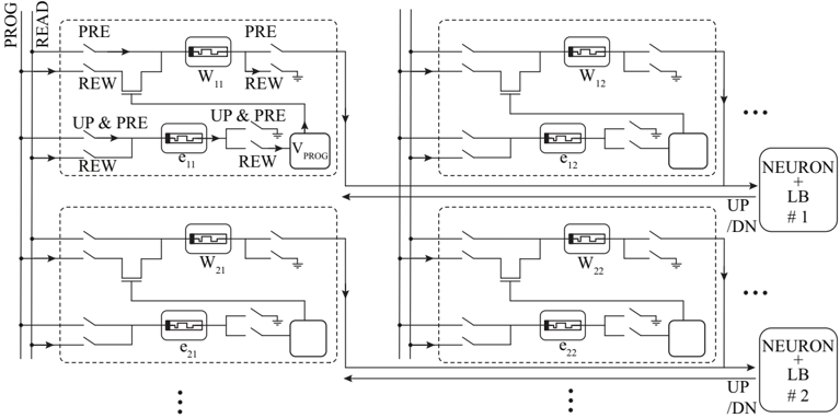
### Visual Description
## Diagram: Neural Network Architecture
### Overview
The image depicts a schematic diagram of a neural network architecture, likely a memory-based or neuromorphic computing system. It shows interconnected blocks representing neurons and associated logic gates, with signals labeled "PRE", "REW", "UP & PRE", "UP/DN", and "PROG". The diagram appears to illustrate the flow of signals during programming (PROG) and read operations (READ). The structure is repeated, suggesting a multi-layered or array-based implementation.
### Components/Axes
The diagram consists of repeating blocks, each representing a neuron and associated circuitry. Key labels include:
* **PROG/READ:** Input signal indicating programming or read mode. Located on the left vertical edge.
* **PRE:** Precharge signal.
* **REW:** Read/Write enable signal.
* **UP & PRE:** Combined Up and Precharge signal.
* **UP/DN:** Up/Down signal.
* **W<sub>ij</sub>:** Weighting element (likely a transistor or resistive element). Subscripts 'ij' denote the connection between neurons.
* **c<sub>ij</sub>:** Capacitive element (likely a capacitor). Subscripts 'ij' denote the connection between neurons.
* **NEURON + LB #1 & #2:** Labels indicating neuron blocks with local buffering.
* The diagram is structured in a grid-like fashion, with rows and columns of neuron blocks.
* Ground symbol (represented by a triangle pointing downwards) is present in multiple locations.
### Detailed Analysis or Content Details
The diagram shows a repeating pattern of neuron blocks. Let's analyze one block in detail:
1. **Input Signals:** The block receives signals "PRE", "REW", and "UP & PRE" from the left. "PROG" is also present.
2. **Weighting Element (W<sub>ij</sub>):** A transistor-like element labeled "W<sub>ij</sub>" is connected to the "PRE" signal. This likely represents a synaptic weight.
3. **Capacitive Element (c<sub>ij</sub>):** A capacitor-like element labeled "c<sub>ij</sub>" is connected to the "REW" signal. This likely stores charge representing the neuron's state.
4. **Logic Gates:** Logic gates (AND-like symbols) combine signals "UP" and "PRE" to control the flow of current.
5. **Output Signal:** The block outputs the "UP/DN" signal to the next neuron block.
6. **Repetition:** The pattern repeats horizontally and vertically, forming an array of neurons. The "..." notation indicates that the array continues beyond the visible portion of the diagram.
The diagram shows the following signal flow:
* **Programming (PROG):** The "PROG" signal likely controls the writing of information into the capacitive element "c<sub>ij</sub>" via the "REW" signal and weighting element "W<sub>ij</sub>".
* **Reading (READ):** During read mode, the "PRE" signal charges the capacitive element, and the "REW" signal reads the stored charge. The "UP/DN" signal represents the output of the neuron.
### Key Observations
* The diagram emphasizes the interplay between precharge, read/write, and up/down signals in controlling the neuron's behavior.
* The use of weighting elements (W<sub>ij</sub>) and capacitive elements (c<sub>ij</sub>) suggests a memory-based or analog computing approach.
* The repeating structure indicates a scalable architecture.
* The diagram does not provide specific numerical values for the components or signals. It is a conceptual representation of the architecture.
### Interpretation
The diagram illustrates a neural network architecture that leverages analog memory elements (capacitors) and weighted connections (transistors) to perform computations. The "PROG/READ" signal suggests a dynamic system where the network can be programmed with specific weights and then used for inference. The "UP/DN" signal likely represents the neuron's activation level.
The architecture appears to be designed for efficient energy consumption and scalability. The use of local buffering ("LB") suggests an attempt to reduce the impact of parasitic capacitances and improve signal integrity. The diagram highlights the fundamental building blocks of a neuromorphic computing system, where computation is performed using physical properties of the hardware rather than purely digital logic.
The diagram is a high-level representation and does not provide details about the specific implementation of the transistors, capacitors, or logic gates. It focuses on the overall signal flow and the key components of the architecture. The absence of numerical values suggests that the diagram is intended to convey the conceptual design rather than a precise engineering specification. The diagram is a conceptual illustration of a neural network architecture, likely for research or educational purposes.
</details>
## 3 . 3 . 4 . 2 Circuit Simulation
Fig. 3 . 16 describes the block diagram of the LB implementing SDSP rule, which calculates the prepost neurons' correlation. The membrane variable (described here as a current Imem since circuits are in current-mode) is compared against a threshold value I th through a Bump circuit [ 143 , 224 ].
The output of this block is digitized through a current comparator (in our design chosen as a Winner-Take-All (WTA) block [ 225 ]) and generates UP / DN signals if the membrane variable is above/below the threshold I th , and STOP, SP , if they are close within the dead zone of the bump circuit [ 224 ].
Fig. 3 . 16 b presents the circuit schematic which reads the PCM-trace and generates VPROG . To read the state of the device, a voltage divider is formed between the PCM device and a pseudo resistor, highlighted in green. As the device resistance changes, the input voltage to the differential pair, highlighted in red, changes. This change is amplified by the gain of the diff. pair and the device current is normalized to its tail current giving rise to IPROG
F igure 3 . 16 : (a) Learning block diagram generating UP/DN signals as a function of the correlation between pre and post-synaptic activity. (b) VPROG circuit reading from the eligibility trace device through the voltage divider (green) and generating IPROG through the diff. pair (red) to program the weight device.
<details>
<summary>Image 24 Details</summary>
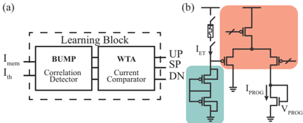
### Visual Description
\n
## Diagram: Learning Block and Circuit Schematic
### Overview
The image presents a schematic diagram of a learning block and a corresponding circuit implementation. Part (a) shows a block diagram of the learning block, while part (b) details the circuit schematic. The diagram appears to relate to neuromorphic computing or analog machine learning.
### Components/Axes
**Part (a): Learning Block**
* **Inputs:** I<sub>mem</sub>, I<sub>th</sub>
* **Internal Blocks:** BUMP, Correlation Detector, WTA (Winner-Take-All), Current Comparator
* **Outputs:** UP, SP, DN
* **Label:** "Learning Block" enclosed in a dashed rectangle.
**Part (b): Circuit Schematic**
* **Inputs:** I<sub>ET</sub>, I<sub>PROG</sub>, V<sub>PROG</sub>
* **Components:** MOSFETs (transistors), Switch
* **Color Coding:** Teal (bottom section), Peach/Salmon (top section)
* **Labels:** I<sub>ET</sub>, I<sub>PROG</sub>, V<sub>PROG</sub>, UP, SP, DN
### Detailed Analysis or Content Details
**Part (a): Learning Block**
The learning block receives two inputs: I<sub>mem</sub> and I<sub>th</sub>. These inputs feed into a "BUMP" block, which then connects to a "Correlation Detector". The output of the Correlation Detector is fed into a "Current Comparator" along with the output of the "WTA" block. The Current Comparator produces three outputs: UP, SP, and DN. The function of each block is not explicitly defined in the diagram, but the names suggest their roles in a learning process.
**Part (b): Circuit Schematic**
The circuit schematic consists of several MOSFETs arranged in a specific configuration. The top section (peach/salmon) contains a series of transistors connected to a voltage source. A switch controls the connection between I<sub>ET</sub> and the top section. The bottom section (teal) consists of a stack of transistors connected to ground. The schematic shows connections for I<sub>PROG</sub> and V<sub>PROG</sub>. The outputs UP, SP, and DN are connected to the circuit. The schematic appears to implement the functionality of the learning block described in part (a).
### Key Observations
* The diagram uses a block diagram approach for the learning block (part a) and a detailed circuit schematic for its implementation (part b).
* The color coding in part (b) may indicate different functional sections or signal paths within the circuit.
* The outputs UP, SP, and DN are consistent between the block diagram and the circuit schematic, suggesting they represent the same signals.
* The diagram does not provide specific values for currents or voltages, only labels.
### Interpretation
The diagram illustrates a potential hardware implementation of a learning block. The "BUMP" and "Correlation Detector" blocks likely perform some form of signal processing to detect patterns or correlations in the input signals. The "WTA" block selects the strongest signal, and the "Current Comparator" compares the selected signal with a threshold or reference signal. The outputs UP, SP, and DN likely control the adjustment of synaptic weights or other parameters in a learning system. The circuit schematic in part (b) provides a possible analog circuit implementation of this learning block, using MOSFETs to perform the necessary computations. The diagram suggests a neuromorphic approach to machine learning, where analog circuits are used to mimic the behavior of biological neurons and synapses. The lack of specific values suggests this is a conceptual diagram rather than a detailed design specification. The diagram is a high-level representation of a learning system, and further details would be needed to fully understand its functionality.
</details>
which develops VPROG through the diode-connected NMOS transistor. VPROG is connected to the gate of the transistor in series with the weight PCM (see Fig. 3 . 15 ).
Fig. 3 . 17 a plots PRE, Imem , the output of the learning block at the time of the PRE, and the gradual
<details>
<summary>Image 25 Details</summary>
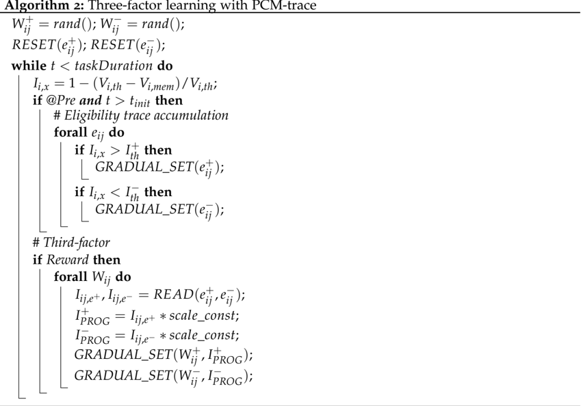
### Visual Description
\n
## Algorithm: Three-factor learning with PCM-trace
### Overview
The image presents a pseudocode algorithm titled "Three-factor learning with PCM-trace". It outlines a learning process involving iterative updates based on eligibility traces and reward signals. The algorithm is structured as a `while` loop with nested `if` and `for all` statements, indicating a sequential and iterative process.
### Components/Axes
There are no axes or traditional chart components. The structure is purely textual, representing a computational algorithm. Key variables and functions are:
* `Wᵢⱼ⁺`: Positive weight.
* `Wᵢⱼ⁻`: Negative weight.
* `eᵢⱼ⁺`: Positive eligibility trace.
* `eᵢⱼ⁻`: Negative eligibility trace.
* `Iᵢₓ`: Input index.
* `Vᵢ,th`: Threshold value.
* `Vᵢ,mem`: Memory value.
* `t`: Time step.
* `taskDuration`: Total duration of the task.
* `tᵢnit`: Initialization time.
* `Iᵢ,th`: Input threshold.
* `Iᴾᴿᴼᶜ`: Processed input.
* `scale_const`: Scaling constant.
* `READ(eᵢⱼ⁺, eᵢⱼ⁻)`: Function to read eligibility traces.
* `GRADUAL_SET(variable)`: Function to gradually set a variable.
* `RESET(variable)`: Function to reset a variable.
* `@Pre`: Condition for pre-processing.
* `Reward`: Condition for reward processing.
### Detailed Analysis / Content Details
The algorithm can be broken down as follows:
1. **Initialization:**
* `Wᵢⱼ⁺ = rand(); Wᵢⱼ⁻ = rand();`: Initialize positive and negative weights randomly.
* `RESET(eᵢⱼ⁺); RESET(eᵢⱼ⁻);`: Reset positive and negative eligibility traces.
2. **Main Loop:** `while t < taskDuration do`
* `Iᵢₓ = 1 − (Vᵢ,th − Vᵢ,mem) / Vᵢ,th;`: Calculate the input index `Iᵢₓ`.
* `if @Pre and t > tᵢnit then`: Check if the pre-processing condition is met and the time step is greater than the initialization time.
* `# Eligibility trace accumulation`: Comment indicating eligibility trace accumulation.
* `forall eᵢⱼ do`: Iterate over all eligibility traces.
* `if Iᵢₓ > Iᵢ,th then`: If the input index is greater than the input threshold.
* `GRADUAL_SET(eᵢⱼ⁺);`: Gradually set the positive eligibility trace.
* `if Iᵢₓ < Iᵢ,th then`: If the input index is less than the input threshold.
* `GRADUAL_SET(eᵢⱼ⁻);`: Gradually set the negative eligibility trace.
* `# Third-factor`: Comment indicating the third-factor processing.
* `if Reward then`: Check if a reward is received.
* `forall Wᵢⱼ do`: Iterate over all weights.
* `Iᵢⱼ₋⁺, Iᵢⱼ₋⁻ = READ(eᵢⱼ⁺, eᵢⱼ⁻);`: Read the positive and negative eligibility traces.
* `Iᴾᴿᴼᶜ₋⁺ = Iᵢⱼ₋⁺ * scale_const;`: Calculate the processed positive input.
* `Iᴾᴿᴼᶜ₋⁻ = Iᵢⱼ₋⁻ * scale_const;`: Calculate the processed negative input.
* `GRADUAL_SET(Wᵢⱼ⁺, Iᴾᴿᴼᶜ₋⁺);`: Gradually set the positive weight using the processed positive input.
* `GRADUAL_SET(Wᵢⱼ⁻, Iᴾᴿᴼᶜ₋⁻);`: Gradually set the negative weight using the processed negative input.
### Key Observations
The algorithm combines elements of reinforcement learning (reward signal) with eligibility traces to update weights. The use of separate positive and negative weights and eligibility traces suggests a mechanism for handling both reinforcement and punishment signals. The `GRADUAL_SET` function implies a learning rate or smoothing factor is applied during weight updates. The `READ` function suggests that the eligibility traces are being accessed for use in weight updates.
### Interpretation
This algorithm appears to implement a form of reinforcement learning where the weights are adjusted based on the reward received and the eligibility traces of the associated actions. The eligibility traces act as a short-term memory of recent actions, allowing the algorithm to credit or blame those actions for the received reward. The "third-factor" component, involving the `READ` function and processed inputs, likely introduces a more nuanced weighting scheme based on the magnitude of the eligibility traces. The use of `scale_const` suggests a control over the impact of the eligibility traces on the weight updates. The algorithm's structure suggests it is designed for continuous learning in an environment where rewards are sparse or delayed. The `GRADUAL_SET` function is crucial for stability, preventing drastic weight changes that could disrupt learning. The algorithm is a sophisticated approach to learning, combining several key concepts from reinforcement learning and neural networks.
</details>
SET pulse applied to the device. As shown, the UP signal is asserted when the membrane current is higher than the threshold indicated in red, which causes a gradual SET pulse with 100 µA to be applied across the PCM-trace device upon PRE events. Fig 3 . 17 b shows the generated IPROG as a function of the state of the eligibility trace device. The higher the ET device's resistance, the less the accumulated correlation, thus the lower the programming current that should be applied to the weight device. The resistance on the x axis of the plot matches the measured resistance of PCM devices shown in Fig. 3 . 11 .
## 3 . 3 . 5 Discussion
Long-lasting ETs enable the construction of powerful learning mechanisms for solving complex tasks by bridging the synaptic and behavioral time-scales. In this work, for the first time, we proposed to use the drift of PCM devices to implement ETs, and analyzed their feasibility for implementation in existing fabrication technologies.
The implementation of the three-factor learning rules with ETs per synapse requires complex memory structures for keeping track of the eligibility trace and the weight. Our proposed approach has clear advantages for scaling. Table 3 . 4 shows a comparison between our PCM synapse and a CMOS-only implementation in 22 nm FDSOI technology from [ 226 ].
PCM is among the most advanced emerging memory technology integrated into the neuromorphic domain [ 109 ]. Our approach of using PCM to store both the synaptic weight and the eligibility trace requires no additional nano-fabrication methods.
| | Area ( µm 2 ) | τ ( s ) | Area/ τ ( µm 2 s - 1 ) |
|-----------------|-----------------|-----------|--------------------------|
| CMOS [ 226 ] | 20 × 17 | 6 | 56.6 |
| PCM [This work] | 12 12 | > 30 | < 4.8 |
×
T able 3 . 4 : Area comparison of eligibility trace implementation
<details>
<summary>Image 26 Details</summary>
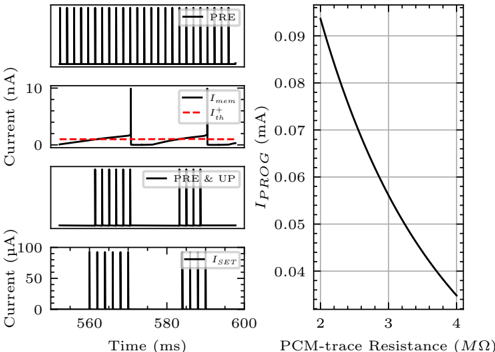
### Visual Description
## Charts/Graphs: Current vs. Time and Program Current vs. Resistance
### Overview
The image presents two distinct charts. The left side displays four time-series plots of current (in nA and µA) versus time (in milliseconds). The right side shows a single plot of program current (I_PROG, in mA) versus PCM-trace resistance (in MΩ). The left charts appear to illustrate different current profiles during a process labeled "PRE" and "UP", while the right chart shows the relationship between program current and resistance.
### Components/Axes
**Left Charts:**
* **X-axis:** Time (ms), ranging from approximately 560 ms to 600 ms.
* **Y-axis (Top & Third Charts):** Current (nA), ranging from 0 to approximately 10 nA.
* **Y-axis (Bottom Chart):** Current (µA), ranging from 0 to approximately 100 µA.
* **Legends:**
* "PRE" (Solid black line)
* "I_mem" (Solid black line)
* "I_th" (Dashed red line)
* "PRE & UP" (Solid black line)
* "I_SET" (Solid black line)
**Right Chart:**
* **X-axis:** PCM-trace Resistance (MΩ), ranging from approximately 2 MΩ to 4 MΩ.
* **Y-axis:** I_PROG (mA), ranging from approximately 0.04 mA to 0.09 mA.
### Detailed Analysis or Content Details
**Left Charts:**
* **Top Chart ("PRE"):** The "PRE" signal is a series of approximately equally spaced, short pulses. The pulses are roughly 0.5 ms wide and occur approximately every 1.5 ms. The amplitude of the pulses is around 5 nA.
* **Second Chart (I_mem & I_th):** "I_mem" starts at approximately 0 mA and gradually increases to around 2 nA by 600 ms. "I_th" remains relatively constant at approximately 0.5 nA until around 580 ms, then increases to approximately 1.5 nA by 600 ms.
* **Third Chart ("PRE & UP"):** This chart shows a similar pattern to the top chart ("PRE") for the first part, then transitions to a series of wider pulses with a higher amplitude. The pulses are approximately 2 ms wide and occur approximately every 3 ms. The amplitude of these pulses is around 5 nA.
* **Bottom Chart ("I_SET"):** The "I_SET" signal consists of a series of short, high-amplitude pulses. The pulses are approximately 0.5 ms wide and occur approximately every 1.5 ms. The amplitude of the pulses is around 80 µA.
**Right Chart (I_PROG vs. PCM-trace Resistance):**
* The line slopes downward, indicating an inverse relationship between program current and PCM-trace resistance.
* At approximately 2 MΩ resistance, the program current is approximately 0.09 mA.
* At approximately 4 MΩ resistance, the program current is approximately 0.04 mA.
* The relationship appears approximately linear.
### Key Observations
* The left charts show different current profiles associated with "PRE", "UP", and "SET" operations.
* The "PRE" signal appears to be a series of small pulses.
* The "PRE & UP" signal combines the "PRE" pulses with larger pulses, suggesting a transition or change in state.
* The "I_SET" signal is characterized by high-amplitude pulses.
* The right chart demonstrates that as the PCM-trace resistance increases, the required program current decreases.
### Interpretation
The data suggests a process involving phase-change memory (PCM) where different current profiles are used to control the state of the memory cell. The "PRE" signal likely prepares the cell for a change, while the "UP" signal initiates the change. The "I_SET" signal is used to set the cell to a specific resistance state. The right chart shows the relationship between the program current and the resulting resistance of the PCM trace. The inverse relationship indicates that higher resistance requires lower program current, and vice versa. This is consistent with the physics of PCM, where higher resistance corresponds to an amorphous state and lower resistance to a crystalline state. The "I_mem" and "I_th" curves likely represent the memory current and threshold current, respectively, and their gradual increase suggests a change in the cell's properties over time. The combination of these signals and their relationship to resistance provides insight into the control and operation of a PCM device.
</details>
Ω)
F igure 3 . 17 : a) From the top: PRE events, POST membrane current ( Imem ) and learning threshold ( I th ), PRE events only when Imem is higher than I th , and corresponding gradual SET current pulse applied to PCM-trace. b) Programming current to be applied to the weight PCM as a function of eligibility trace state.
<details>
<summary>Image 27 Details</summary>

### Visual Description
Icon/Small Image (61x85)
</details>
## DISCOVERING SINGLE MATERIAL THAT SWITCHES BETWEEN VOLATILE OR NON-VOLATILE MODES
This chapter's content was published in Nature Communications, featured as one of 50 best papers recently published in the field and can be found online in an extended form including all experimental details which we omit here for clarity. The original publication is authored by Yigit Demirag ∗ , Rohit Abraham John ∗ , Yevhen Shynkarenko, Yuliia Berezovska, Natacha Ohannessian, Melika Payvand, Peng Zeng, Maryna I. Bodnarchuk, Frank Krumeich, Gökhan Kara, Ivan Shorubalko, Manu V. Nair, Graham A. Cooke, Thomas Lippert, Giacomo Indiveri and Maksym V. Kovalenko.
∗ These authors contributed equally.
Many in-memory computing frameworks demand electronic devices with specific switching characteristics to achieve the desired level of computational complexity. Existing memristive devices cannot be reconfigured to meet the diverse volatile and non-volatile switching requirements, and hence rely on tailored material designs specific to the targeted application, limiting their universality. "Reconfigurable memristors" that combine both ionic diffusive and drift mechanisms could address these limitations, but they remain elusive. Here we present a reconfigurable halide perovskite nanocrystal memristor that achieves ondemand switching between diffusive/volatile and drift/non-volatile modes by controllable electrochemical reactions. Judicious selection of the perovskite nanocrystals and organic capping ligands enable state-of-the-art endurance performances in both modes - volatile ( 2 × 10 6 cycles) and non-volatile ( 5.6 × 10 3 cycles ) . We demonstrate the relevance of such proofof-concept perovskite devices on a benchmark reservoir network with volatile recurrent and non-volatile readout layers based on 19 , 900 measurements across 25 dynamically-configured devices.
## 4 . 1 introduction
The human brain operating at petaflops consumes less than 20 W, setting a precedent for scientists that real-time, ultralow-power data processing in a small volume is possible. Inspired by the human brain, the field of neuromorphic computing attempts to emulate various computational principles of the biological substrate by engineering unique materials [ 227 -229 ] and circuits [ 29 , 230 , 231 ]. In the context of hardware implementation of neural networks, the discovery of memristors has been one of the main driving forces for highly efficient in-memory realizations of synaptic operations. Similar to evolution optimizing neurons and synapses by exploiting stable and metastable molecular dynamics [ 232 ], memristive devices of various physical mechanisms [ 25 , 233 , 234 ] have been discovered and developed with different volatile and non-volatile specifications. Since their inception, memristors have been utilized to implement a wide gamut of applications [ 235 ] such as stochastic computing [ 236 ], hyperdimensional computing [ 237 ], spiking [ 238 ] and artificial neural networks [ 95 ]. However, many of these frameworks often demand very different hardware specifications [ 16 ] (Fig. 1 a). To meet these specifications, the memristor fabrication processes are often tediously engineered to reflect the requirements of targeted neural network configurations (e.g., neural encoding, synaptic precision, etc.). For example, the latest state-of-the-art spiking neural network (SNN) models [ 75 , 197 ] require memory elements operating at multiple timescales, with both volatile and non-volatile properties (from tens of milliseconds to hours) [ 144 ]. The current approach of optimizing memristive devices to a single requirement hinders the possibility of implementing multiple computational primitives in neural networks and precludes their monolithic integration on the same hardware substrate.
In this regard, the realization of drift and diffusive memristors have garnered significant attention. Drift memristors portraying non-volatile memory characteristics are typically designed using oxide dielectric materials with a soft-breakdown behaviour. In combination with inert electrodes, the switching mechanism is determined by filaments of oxygen vacancies (valence change memory); whereas implementations with reactive electrodes rely on electrochemical
F igure 4 . 1 : (a) Different neural network frameworks demand particular switching characteristics from in-memory computing implementations. For example, delay systems [ 239 ] (dynamical nonlinear systems with delayed feedback such as virtual reservoir networks), should exhibit only a fading memory to process the inputs from the recent past. Such short-term dynamics are best represented by volatile thresholdswitching memristors [ 240 ]. SNNs often demand both volatile and non-volatile dynamics, simultaneously. Synaptic mechanisms requiring STP and eligibility traces [ 241 ] can be implemented using volatile memristors [ 24 , 151 ] whereas synaptic efficacy requires either efficient binary-switching [ 20 ] or analog switching devices. Lastly, ANN performances specifically benefit from non-volatile features such as multi-level bit precision of weights and linear conductance response during the training phase [ 21 , 22 ] (b) A reconfigurable memristor with active control over its diffusive and drift dynamics may be a feasible unifying solution. Schematic of the reconfigurable halide perovskite nanocrystal memristor is shown for reference. We utilize the same active switching material ( CsPbBr3NCs capped with OGB ligands) to implement two distinct types of computation in the RC framework. The volatile diffusive mode exhibiting short-term memory is utilized as the reservoir layer while the non-volatile drift mode exhibiting long-term memory serves as the readout layer.
<details>
<summary>Image 28 Details</summary>
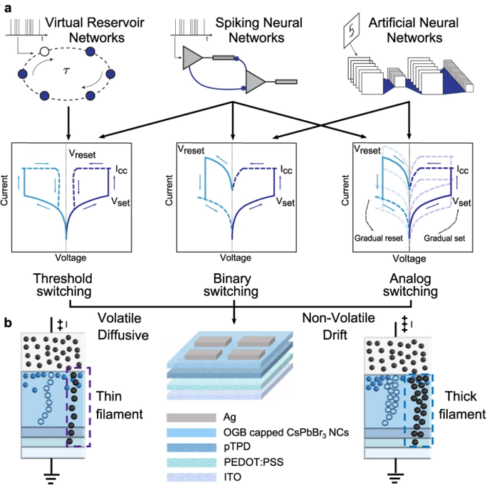
### Visual Description
\n
## Diagram: Neuromorphic Computing Architectures & Switching Mechanisms
### Overview
The image presents a comparison of three types of neural networks (Virtual Reservoir Networks, Spiking Neural Networks, and Artificial Neural Networks) and their corresponding switching mechanisms. The top row depicts schematic representations of each network type. The bottom row illustrates the associated current-voltage (I-V) characteristics and the physical mechanisms underlying the switching behavior. The image is divided into two main sections, labeled 'a' and 'b'. Section 'a' focuses on the network architectures and their I-V curves, while section 'b' details the physical structures and switching mechanisms.
### Components/Axes
**Section a:**
* **Network Types (Top Row):** Virtual Reservoir Networks, Spiking Neural Networks, Artificial Neural Networks.
* **I-V Curves (Bottom Row):** Each curve has a Voltage axis (horizontal) and a Current axis (vertical).
* **I-V Curve Labels:** V<sub>reset</sub>, I<sub>cc</sub>, V<sub>set</sub>, "Gradual reset", "Gradual set".
* **Switching Types (Below I-V Curves):** Threshold switching, Binary switching, Analog switching.
* **Switching Properties (Above I-V Curves):** Volatile Diffusive, Non-Volatile Drift.
**Section b:**
* **Physical Structures:** Depictions of thin filament, layered structures, and thick filament configurations.
* **Material Legend:** Ag, OGB capped CsPbBr<sub>3</sub> NCs, pTPD, PEDOT:PSS, ITO.
* **Electrical Connections:** Ground symbol (inverted triangle).
* **Voltage/Current Arrows:** Indicate the direction of current flow.
### Detailed Analysis or Content Details
**Section a: Network Architectures & Switching**
* **Virtual Reservoir Networks:** The schematic shows a network of interconnected nodes with a time constant denoted by τ. The I-V curve exhibits a threshold switching behavior with a clear V<sub>set</sub> and V<sub>reset</sub>. The current rises sharply after V<sub>set</sub> is reached.
* **Spiking Neural Networks:** The schematic depicts a network with a funnel-like input converging onto a neuron. The I-V curve shows binary switching, with a distinct on/off state. V<sub>reset</sub> and V<sub>set</sub> are indicated.
* **Artificial Neural Networks:** The schematic shows a layered structure of interconnected nodes. The I-V curve demonstrates analog switching, with a gradual set and reset behavior. The current changes smoothly with voltage.
**Section b: Physical Structures & Switching Mechanisms**
* **Volatile Diffusive Switching (Left):** A schematic shows a thin filament formed by conductive nanoparticles within an insulating matrix. The filament is connected to a voltage source and ground. The legend indicates the materials: Ag, OGB capped CsPbBr<sub>3</sub> NCs, pTPD, PEDOT:PSS, ITO.
* **Non-Volatile Drift (Right):** A schematic shows a thick filament formed by conductive nanoparticles within an insulating matrix. The filament is connected to a voltage source and ground. The legend indicates the materials: Ag, OGB capped CsPbBr<sub>3</sub> NCs, pTPD, PEDOT:PSS, ITO.
* **Layered Structure (Center):** A schematic shows a layered structure with Ag, OGB capped CsPbBr<sub>3</sub> NCs, pTPD, PEDOT:PSS, and ITO layers.
### Key Observations
* The three network types are linked to distinct switching mechanisms. Virtual Reservoir Networks utilize threshold switching, Spiking Neural Networks employ binary switching, and Artificial Neural Networks leverage analog switching.
* The volatile diffusive switching mechanism involves a thin filament, while the non-volatile drift mechanism utilizes a thick filament.
* The material stack in section 'b' is consistent across all three structures, suggesting a common material platform for implementing these switching mechanisms.
* The I-V curves are qualitatively different, reflecting the different switching behaviors.
### Interpretation
This diagram illustrates the relationship between different neuromorphic computing architectures and the underlying physical mechanisms that enable their functionality. The choice of switching mechanism (threshold, binary, or analog) directly impacts the computational capabilities of the corresponding neural network. The use of metal-organic halide perovskite (CsPbBr<sub>3</sub> NCs) suggests a focus on emerging materials for neuromorphic applications. The distinction between volatile and non-volatile switching highlights the trade-offs between memory retention and energy efficiency. The diagram suggests a pathway for designing and implementing neuromorphic systems by carefully selecting the appropriate network architecture and switching mechanism based on the desired application requirements. The layered structure in the center of section 'b' likely represents a device used to demonstrate the switching mechanisms on either side. The consistent material stack suggests a common fabrication process for all three devices. The diagram is a conceptual overview and does not provide quantitative data on device performance.
</details>
reactions to form conductive bridges (electrochemical metallization memory) [ 242 ]. Such driftbased memristors fit well for emulating synaptic weights that stay stable between weight updates. In contrast, diffusive memristors are often built with precisely embedded clusters of metallic ions with low diffusion activation energy within a dielectric matrix [ 234 ]. The large availability of such mobile ionic species and their low diffusion activation energy facilitate spontaneous relaxation to the insulating state upon removing power, resulting in volatile threshold switching. Memristive devices with such short-term volatility, are better suited to process temporally-encoded input patterns [ 243 ]. Hence, the application determines the type of volatility, bit-precision or endurance of the memristors, which are then heavily tailored by tedious material design strategies to meet these demands [ 16 ]. For example, deep neural network (DNN) inference workloads require linear conductance response over a wide dynamic range for optimal weight update and minimum
noise for gradient calculation [ 21 , 22 , 95 ]. Whereas SNNs often demand richer and multiple synaptic dynamics simultaneously e.g., short term conductance decay (to implement synaptic cleft phenomena such Ca 2 +-dependent short-term plasticity (STP) and CAMKII-related eligibility traces [ 244 ]), non-volatile device states (to represent synaptic efficacy) and a probabilistic nature (to mimic synaptic vesicle releases [ 243 ]) (Fig. 1 a). However, optimizing the active memristive material for each of these features limits their feasibility to suit a wide range of computational frameworks and ultimately increases the system complexity for most demanding applications. Moreover, these diverse specifications cannot always be implemented by combining different types of memristors on a monolithic circuit e.g., volatile and non-volatile, binary and analog, due to the incompatibility of the fabrication processes. Therefore, the lack of universality of memristors that realize not only one, but diverse computational primitives is an unsolved challenge today.
A reconfigurable memristive computing substrate that allows active control over their ionic diffusive and drift dynamics can offer a viable unifying solution but is hitherto undemonstrated. Although dual-functional memory behaviour has been observed previously, the dominance of one of the mechanisms often results in poor switching performance for either one or both modes, limiting the employability of such devices for demanding applications [ 96 , 97 ]. To the best of our knowledge, there is no report yet of a reconfigurable memristive material that can portray both volatile diffusive and multi-state non-volatile drift kinetics, exhibit facile switching between these two modes, and still pertain excellent performance.
Here we report a reconfigurable memristor computing substrate based on halide perovskite nanocrystals that achieves on-demand switching between volatile and non-volatile modes by encompassing both diffusive and drift kinetics (Fig. 1 b). Halide perovskites are newcomer optoelectronic semiconducting materials that have enabled state-of-the-art solar cells [ 245 ], solid state light emitters [ 246 , 247 ] and photodetectors [ 248 -250 ].Recently, these materials have attracted significant attention as memory elements due to their rich variety of charge transport physics that supports memristive switching, such as modulatable ion migration [ 251 -253 ], electrochemical metallization reactions with metal electrodes [ 254 ] and localized interfacial doping with charge transport layers [ 255 ]. While most reports are based on thin films or bulk crystals of halide perovskites [ 251 -253 , 256 ], interestingly perovskite nanocrystal (NC)-based formulations have been much less investigated till date [ 244 , 257 ]. NCs in general are recently garnering significant attention for artificial synaptic implementations because they support a wide range of switching physics such as trapping and release of photogenerated carriers at dangling bonds over a broad spectral region [ 258 ], and single-electron tunnelling [ 259 ]. They allow low-energy (< fJ), highspeed (MHz) operation, and can support scalable and CMOS-compatible fabrication processes. In the case of perovskite NCs, however, existing implementations often utilize NCs only as a charge trapping medium to modulate the resistance states of another semiconductor, in flash-like configurations a.k.a synaptic transistor [ 260 -263 ]. The memristive switching capabilities and limits of the perovskite NC active matrix remains unaddressed, entailing significant research in this direction. Colloids of perovskite nanocrystals (NCs) are readily processable into thin-film NC solids and they offer a modular approach to impart mesoscale structures and electronic interfaces, tunable by adjusting the NC composition, size and surface ligand capping.
Our device comprises all-inorganic cesium lead bromide ( CsPbBr3 ) NCs capped with organic ligands as the active switching matrix and silver ( Ag ) as the active electrode. The design principle for realizing reconfigurable memristors revolves around two main factors. (i) From a material selection perspective, the low activation energy of migration of Ag + and Br -allows easy formation of conductive filaments. The soft lattice of the halide perovskite NCs facilitates diffusion of the mobile ions. Moreover, the organic capping ligands help regulate the extent of electrochemical reactions, resulting in high endurance and good reconfigurability. (ii) From a peripheral circuit design perspective, active control of the compliance control ( Icc ) determines the magnitude of flux of the mobile ionic species and in turn allows facile switching between volatile diffusive and multi-bit non-volatile drift modes of operation.
The surface capping ligands are observed to play a vital role in determining the switching characteristics and endurance performance. CsPbBr3NCs capped with didodecyldimethylammonium bromide (DDAB) ligands display poor switching performance in both volatile ( 10 cycles) and non-volatile ( 50 cycles) modes, whereas NCs capped with oleylguanidinium bromide (OGB)
ligands exhibit record-high endurance performances in both volatile ( 2 million cycles) as well as non-volatile switching ( 5655 cycles) modes [ 240 , 255 , 264 ]
To validate our approach and demonstrate the advantages of such reconfigurable memristive materials, we use a benchmark model of a fully-memristive reservoir computing (RC) framework interfaced to an artificial neural network (ANN) [ 240 ]. The reservoir is modelled as a network of recurrently-connected units whose dynamics act as short-term memory. Any temporal signal entering the reservoir is subject to a high-dimensional nonlinear transformation that enhances the separability of its temporal features. A linear read-out ANN layer is then connected to the reservoir units with all-to-all connections and trained to perform classification based on the temporal information maintained in the reservoir. Our RC implementation comprises perovskite memristors that are configured as diffusion-based volatile dynamic elements to implement the reservoir nodes and as drift-based non-volatile weights to implement the readout ANN layer. In their diffusive mode, the low activation energy of ion migration of the mobile ionic species ( Ag + and Br -) enables volatile threshold switching. The resulting short-term dynamics are essential for capturing temporal correlations within the input data stream. In the drift mode, stable conductive filaments formed by the drift of the ionic species facilitate programming of non-volatile synaptic weights in the readout layer for both training and inference. Furthermore, the readout layer can be trained online via active regulation of the Icc which allows precise selection of the drift dynamics and enables multiple-bit resolution in the low resistive state (LRS). Using neural firing patterns, we show via both experiments and simulations that a RC framework based on reconfigurable perovskite memristors can accurately extract features in the temporal signals and classify firing patterns.
## 4 . 2 diffusive mode of the perovskite reconfigurable memristor
We investigate two systems for diffusive dynamics-didodecyldimethylammonium bromide (DDAB) and oleylguanidinium bromide (OGB)-capped CsPbBr3NCs. The device structure comprises indium tin oxide (ITO), poly( 3 , 4 -ethylenedioxythiophene) polystyrene sulfonate (PEDOT:PSS), poly(N,N'-bis4 -butylphenyl-N,N'-bisphenyl)benzidine (polyTPD), CsPbBr3NCs and Ag (see 'Methods" section). With an lcc of 1 µ A, both material systems portray volatile threshold switching characteristics with diffusive dynamics and spontaneous relaxation back to the initial state, albeit with contrasting endurance. The DDAB-capped perovskite NCs exhibit a poor on-off ratio (volatile memory a.k.a. VM Ipower ON /Ipower OFF ∼ 10 ) and quick transition to a non-volatile state, resulting in an inferior volatile endurance of ∼ 10 cycles. On the other hand, the OGB-capped perovskite NCs depict a highly robust threshold switching behaviour with sub1 V set voltages, VM Ipower ON /Ipower OFF ∼ 10 3 and a record volatile endurance of 2 × 10 6 cycles (Fig. 3 a). The volatile threshold switching behaviour can be attributed to the redistribution of Ag + and Br -ions under an applied electric field, and their back-diffusion upon removing power [ 253 , 265 , 266 ]. It is also important to note that both these devices exhibit a unidirectional DC threshold switching behaviour with no switching occurring under reverse bias (negative voltage on the Ag electrode). This can be correlated to the dominant bipolar electrode effect over thermal-driven diffusion, in alignment with literature [ 267 -269 ]
## 4 . 3 drift mode of the perovskite reconfigurable memristor
Upon increasing the Icc to 1 mA, both the DDAB and OGB-capped CsPbBr3 NC memristors portray typical non-volatile bipolar resistive switching characteristics, once again with contrasting endurance (Fig. 4 . 2 , Fig. 4 . 3 and Supplementary Fig. A. 22 ). Both systems depict forming-free operations and similar on-off ratios ( ≥ 10 3 ) . However, the DDAB capped perovskite NCs quickly transit to a non-erasable non-volatile state, resulting in an inferior non-volatile endurance of 50 cycles (Supplementary Fig. A. 23 ). On the other hand, the OGB-capped perovskite NC-based memristor portrays a highly robust switching behaviour with sub- 1 V set voltages, and record-high non-volatile endurance and retention of 5655 cycles and 10 5 s, respectively (Fig. 4 . 3 , Supplementary Fig. A. 24 ). Similar to the volatile threshold switching mechanism, the nonvolatile resistive
F igure 4 . 2 : The device structure comprises ITO ( 100 nm), PEDOT:PSS ( 30 nm), polyTPD ( 20 nm), OGBcapped CsPbBr3NCs ( 20 nm ) and Ag ( 150 nm ) . (a) Diffusive mode- illustration of the proposed volatile diffusive switching mechanism. (b) Drift mode-illustration of the proposed non-volatile drift switching mechanism. Additional note: The thickness of the individual layers in the device schematic are not drawn to scale to match the experimentally-measured thicknesses. The perovskite layer is not a bulk semiconductor, but 1 -2 layers of nanocrystals (NCs). The schematic is drawn for simplicity, to illustrate the formation and rupture of conductive filaments (CFs) of Ag through the device structure.
<details>
<summary>Image 29 Details</summary>
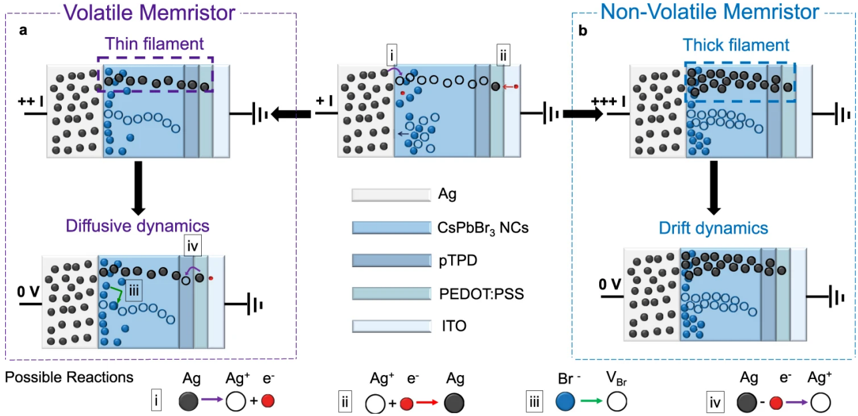
### Visual Description
\n
## Diagram: Memristor Dynamics - Volatile vs. Non-Volatile
### Overview
The image presents a comparative diagram illustrating the dynamics of volatile and non-volatile memristors. It depicts the structural changes and ion movement within these devices under different voltage conditions. The diagram is split into two main sections (a and b), representing volatile and non-volatile memristors respectively. Each section shows a series of states representing the device's behavior under positive voltage, zero voltage, and the resulting dynamics. A legend at the bottom explains the symbols used to represent ions and vacancies.
### Components/Axes
The diagram consists of layered structures representing the memristor components. These layers are labeled as follows:
* **Ag:** Silver
* **CsPbBr3 NCs:** Cesium Lead Bromide Nanocrystals
* **pTPD:** (likely an organic semiconductor)
* **PEDOT:PSS:** Poly(3,4-ethylenedioxythiophene) polystyrene sulfonate
* **ITO:** Indium Tin Oxide
The diagram also uses symbols to represent ions and vacancies:
* **i:** Ag⁺ + e⁻ (Silver ion plus electron) - Red circle with a plus sign and an electron.
* **ii:** Ag⁺ → Ag (Silver ion transforms to Silver) - Red circle transforming into a black circle.
* **iii:** Br⁻ (Bromide ion) - Blue circle.
* **iv:** VBr (Bromide vacancy) - Yellow circle.
Voltage sources are indicated with "+" and "-" signs, and arrows show the direction of ion movement.
### Detailed Analysis / Content Details
**Section a: Volatile Memristor - Thin Filament**
* **Initial State (Top-Left):** A positive voltage is applied to the structure. Silver ions (Ag⁺, represented by red circles) and electrons (e⁻) are present.
* **Intermediate State (Top-Center):** Silver ions are reduced to silver atoms (Ag, represented by black circles), forming a thin filament. The reaction i (Ag⁺ + e⁻ → Ag) is indicated.
* **Intermediate State (Top-Right):** The filament continues to grow with more silver atoms.
* **Final State (Bottom-Left):** When the voltage is set to 0V, the silver atoms exhibit diffusive dynamics. Silver atoms are shown moving randomly within the structure.
* **Final State (Bottom-Center):** Silver atoms are shown moving randomly within the structure. The reaction iii (Br⁻) is indicated.
* **Final State (Bottom-Right):** Silver atoms are shown moving randomly within the structure. The reaction iv (Ag e⁻ Ag⁺) is indicated.
**Section b: Non-Volatile Memristor - Thick Filament**
* **Initial State (Top-Left):** A positive voltage is applied to the structure. Silver ions (Ag⁺, represented by red circles) and electrons (e⁻) are present.
* **Intermediate State (Top-Center):** Silver ions are reduced to silver atoms (Ag, represented by black circles), forming a thick filament. The reaction i (Ag⁺ + e⁻ → Ag) is indicated.
* **Intermediate State (Top-Right):** The filament continues to grow with more silver atoms.
* **Final State (Bottom-Left):** When the voltage is set to 0V, the silver atoms exhibit drift dynamics. Silver atoms are shown moving in a directed manner within the structure.
* **Final State (Bottom-Center):** Silver atoms are shown moving in a directed manner within the structure. The reaction iii (Br⁻) is indicated.
* **Final State (Bottom-Right):** Silver atoms are shown moving in a directed manner within the structure. The reaction iv (Ag e⁻ Ag⁺) is indicated.
### Key Observations
The key difference between the volatile and non-volatile memristors lies in the dynamics of the silver atoms when the voltage is removed. In the volatile memristor, the silver atoms exhibit diffusive dynamics (random movement), leading to filament dissolution and loss of memory. In the non-volatile memristor, the silver atoms exhibit drift dynamics (directed movement), maintaining the filament structure and preserving the memory state. The filament in the non-volatile memristor is also depicted as being thicker than in the volatile memristor.
### Interpretation
This diagram illustrates the fundamental mechanisms governing the volatility of memristors. The type of ion dynamics (diffusive vs. drift) is directly linked to the stability of the conductive filament and, consequently, the memory retention capability of the device. The thicker filament in the non-volatile memristor likely contributes to its stability by providing more anchoring points and reducing the likelihood of complete dissolution. The reactions i, ii, iii, and iv represent the electrochemical processes involved in the formation and dissolution of the silver filament, driven by the applied voltage and the movement of ions and vacancies within the material. The diagram provides a visual explanation of how material properties and ion dynamics can be engineered to create memristors with desired volatility characteristics. The diagram is a conceptual illustration and does not provide quantitative data. It focuses on the qualitative differences in behavior.
</details>
switching can also be attributed to redistribution of ions, and electrochemical reactions under an applied electric field [ 251 , 252 ]. The larger Icc of 1 mA results in permanent and thicker conductive filamentary pathways, and the switching dynamics is now dominated by the drift kinetics of the mobile ion species Ag + and Br -, rather than diffusion.
In the case of DDAB-capped CsPbBr3NCs, the inferior volatile endurance, quick transition to a non-volatile state and mediocre non-volatile endurance indicates poor control of the underlying electrochemical processes and formation of permanent conductive filaments even at low compliance currents. On the other hand, capping CsPbBr3NCs with OGB ligands enables better regulation of the electrochemical processes, resulting in superior on-off ratio, volatile endurance as well as non-volatile endurance. Scanning Electron Microscope (SEM) images indicate similar film thickness in both devices, ruling out dependence on the active material thickness (Fig. 4 . 3 ). Transmission Electron Microscopy (TEM) and Atomic Force Microscopy (AFM) images reveal similar nanocrystal size ( ∼ 10 nm ) and surface roughness for both films, dismissing variations in crystal size and morphology as possible differentiating reasons (Fig. 4 . 3 and Supplementary Fig. A. 25 ). While the exact mechanism is still unknown, the larger size of the OGB ligands compared to DDAB ( 2.3 nm vs. 1.7 nm ) could intuitively provide better isolation to the CsPbBr3NCs and prevent excess electrochemical redox reactions of Ag + and Br -, modulating the formation and rupture of conductive filaments. This comparison is further supported by photoluminescence measurements, pointing to a larger drop of luminescence quantum yield in the films of DDAB-capped NCs, arising from the stronger excitonic diffusion and trapping.
To probe the mechanism further, devices with Au as the top electrode were fabricated, but did not show any resistive switching behaviour. The devices do not reach the compliance current of 1 mA during the set process and do not portray the sudden increase in current, typical of filamentary memristors. This indicates that Ag is crucial for resistive switching and also proves that Br - ions play a trivial role in our devices if any. Control experiments on PEDOT:PSS only and PEDOT:PSS + pTPD devices further reiterate importance of the perovskite NC thin film as an active matrix for reliable and robust Ag filament formation and rupture. Secondary ion mass spectrometry (SIMS) profiling reveals a clear difference in the 107 Ag cross section profile
F igure 4 . 3 : The device structure comprises ITO ( 100 nm ) , PEDOT:PSS ( 30 nm ) , polyTPD ( 20 nm ) , OGBcapped CsPbBr3NCs ( 20 nm ) and Ag ( 150 nm ) as shown in the SEM cross-section. Thickness of the individual layers were confirmed by AFM. The TEM image reveals NCs with an average diameter of -10 nm. (a) Diffusive mode- evolution of the device conductance upon applying DC sweep voltages ( 0 V → 2 V → 0 V ) with an Icc = 1 µ A (top), endurance performance (bottom). (b) Drift mode- evolution of the device conductance upon applying DC sweep voltages ( 0 V → + 5 V → 0 V → -7 V → 0 V ) with an Icc = 1 mA during SET operation (top), endurance performance (bottom).
<details>
<summary>Image 30 Details</summary>
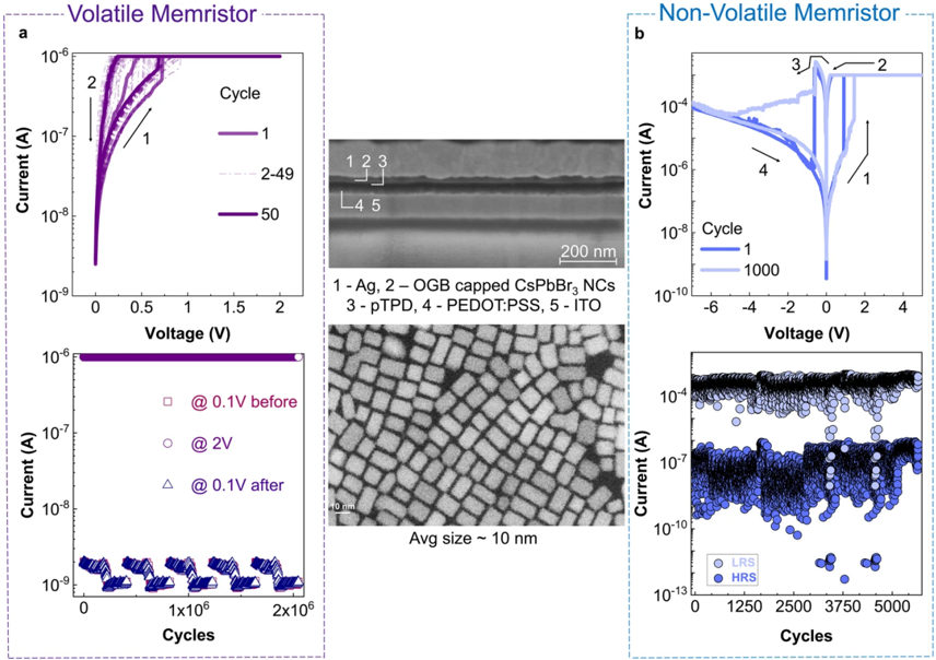
### Visual Description
## Chart/Diagram Type: Memristor Characteristics Comparison
### Overview
The image presents a comparison between volatile and non-volatile memristors, showcasing their current-voltage (I-V) characteristics and endurance (current vs. cycles). The left side (a) focuses on a volatile memristor, while the right side (b) focuses on a non-volatile memristor. A schematic diagram and a transmission electron microscopy (TEM) image are also included to provide structural context.
### Components/Axes
**Volatile Memristor (a):**
* **Top Chart:** I-V curves. X-axis: Voltage (V) from 0 to 1.25. Y-axis: Current (A) on a logarithmic scale from 10^-8 to 10^-6.
* **Bottom Chart:** Current vs. Cycles. X-axis: Cycles from 0 to 2x10^6. Y-axis: Current (A) on a logarithmic scale from 10^-9 to 10^-6.
* **Legend (Top Chart):**
* 1: Cycle 1 (Dark Purple)
* 2-49: Intermediate Cycles (Light Purple)
* 50: Cycle 50 (Red)
* **Legend (Bottom Chart):**
* @ 0.1V before (Purple Squares)
* @ 2V (Light Blue Circles)
* @ 0.1V after (Light Purple Triangles)
**Non-Volatile Memristor (b):**
* **Top Chart:** I-V curves. X-axis: Voltage (V) from -6 to 4. Y-axis: Current (A) on a logarithmic scale from 10^-10 to 10^-4.
* **Bottom Chart:** Current vs. Cycles. X-axis: Cycles from 0 to 5000. Y-axis: Current (A) on a logarithmic scale from 10^-13 to 10^-7.
* **Legend (Top Chart):**
* 1: Cycle 1 (Dark Blue)
* 2: Cycle 2 (Light Blue)
* 3: Cycle 3 (Dark Blue)
* 4: Cycle 4 (Light Blue)
* **Legend (Bottom Chart):**
* LRS: Low Resistance State (Blue Circles)
* HRS: High Resistance State (Orange Circles)
**Schematic Diagram (Center):**
* Labeled layers: 1-Ag, 2-OGB capped CsPbBr3 NCs, 3-ptPD, 4-PEDOT:PSS, 5-ITO. Scale bar: 200 nm.
**TEM Image (Center):**
* Shows a lattice structure. Average size ~ 10 nm.
### Detailed Analysis or Content Details
**Volatile Memristor (a):**
* **Top Chart:** The I-V curves show a hysteresis loop that diminishes with increasing cycles. Cycle 1 (dark purple) exhibits a clear hysteresis. As the cycle number increases (light purple), the hysteresis loop becomes smaller, and by cycle 50 (red), the loop is significantly reduced.
* **Bottom Chart:** The current at 0.1V before cycling is approximately 5x10^-7 A. The current at 2V is approximately 2x10^-6 A. After cycling at 0.1V, the current drops to approximately 2x10^-8 A. The current remains relatively stable over 2 million cycles, with some fluctuations.
**Non-Volatile Memristor (b):**
* **Top Chart:** The I-V curves show a more pronounced hysteresis loop that persists across multiple cycles. Cycle 1 (dark blue) and Cycle 2 (light blue) show a clear switching behavior. The curves exhibit a pinched hysteresis loop.
* **Bottom Chart:** The device alternates between Low Resistance State (LRS) and High Resistance State (HRS). The LRS current is approximately 5x10^-7 A, while the HRS current is approximately 1x10^-11 A. The device shows stable switching between LRS and HRS for up to 5000 cycles.
**Schematic Diagram:**
* The diagram illustrates a layered structure of the memristor, with Ag, CsPbBr3 nanocrystals, ptPD, PEDOT:PSS, and ITO layers.
**TEM Image:**
* The TEM image reveals a lattice structure with an average size of approximately 10 nm.
### Key Observations
* The volatile memristor exhibits a diminishing hysteresis loop with increasing cycles, indicating a loss of memory.
* The non-volatile memristor maintains a stable hysteresis loop and switching behavior between LRS and HRS, demonstrating its non-volatile nature.
* The schematic diagram and TEM image provide insights into the device's structure and nanoscale features.
* The current difference between LRS and HRS in the non-volatile memristor is significant, indicating a clear on/off ratio.
### Interpretation
The data demonstrates a clear distinction between volatile and non-volatile memristor behavior. The volatile memristor's I-V characteristics change significantly with cycling, losing its initial hysteresis and thus its memory capability. This suggests that the resistance state is not retained after repeated switching. In contrast, the non-volatile memristor exhibits stable switching between LRS and HRS, indicating a persistent memory effect. The layered structure shown in the schematic diagram and the nanoscale features observed in the TEM image likely contribute to the observed memristive behavior. The CsPbBr3 nanocrystals are likely the active material responsible for the resistance switching. The difference in performance between the two memristor types highlights the importance of material selection and device architecture in achieving stable non-volatile memory. The large difference in current between LRS and HRS in the non-volatile memristor suggests a high on/off ratio, which is crucial for practical applications.
</details>
when comparing an ON and OFF device. An increase of the 107 Ag count is observed at the interface between the halide perovskite and the organic layers for the device in the ON state. Temperature-dependent measurements further confirm the theory of migration of Ag + ions through the perovskite matrix. The conclusions in this study are observed to be independent of the NC layer thickness, NC size and dispersity.
## 4 . 4 reservoir computing with perovskite memristors
To demonstrate the advantages of the reconfigurability features of our perovskite memristors, we model a fully-memristive RC framework with dynamically-configured layer of virtual volatile reservoir nodes and a readout ANN layer with non-volatile weights in simulation. In particular, we address three distinct forms of computational requirements using the reconfigurability of the proposed device: an accumulating/decaying short-term memory for the temporal processing in the reservoir; a stable long-term memory for retaining trained weights in the readout layer, and a circuit methodology for accessing analog states from binary devices to enhance the training performance.
## 4 . 5 diffusive perovskite memristors as reservoir elements
To implement the reservoir layer with the fabricated memristor devices, we utilize the virtual node concept originally proposed by Appeltant et al. [ 239 ]. Instead of conventional transforming of the input signal to a high-dimensional reservoir state by processing over many non-linear units, the virtual node concept employs the idea of delayed feedback on a single physical device exhibiting strong short-term effects. Under the influence of a sequential input, the dynamical device state goes through a non-linear transient response, which is recorded with fixed timesteps to create a set of virtual nodes representing the reservoir state. Hence, the transient device non-linearity constitutes temporal processing, and the delay system forms the high dimensional representation in the reservoir.
Elements of a reservoir layer should ideally possess a fading memory (sometimes called shortterm memory or echo state property) and non-linear internal dynamics [ 270 ]. The fading memory effect plays a key role in extracting features in the temporal domain of the input data stream, while the non-linear internal dynamics enable projection of temporal features to a high-dimensional state with good separability [ 271 ]. Response of the OGB-capped CsPbBr3NC memristors to low-voltage electrical spikes reveal short-term/fading diffusive dynamics with a relaxation time ≥ 5 ms for an input pulse duration = 20 ms and amplitude = 1 V. Non-linear internal dynamics are evident in 4 formats- (i) from the transient evolution of the device conductance during the stimulations; and from the final device conductance as a function of the applied pulse (ii) amplitude, (iii) width and (iv) number (Supplementary Fig. A. 26 ). An additional test of the echo state property reveals that the present device state is reflective of the input temporal features in the recent past ( < 23 ms ) but not the far past, enabling efficient capture of short-term dependencies in the input data stream (Supplementary Fig. A. 27 ). Stimulation of pulse streams with different temporal features results in distinct temporal dynamics of memristor states.
## 4 . 6 drift perovskite memristors as readout elements
Storing the weight of the fully-connected readout layer of the ANN requires non-volatile synaptic devices. For representing synaptic efficacy, we use the drift-based perovskite memristor configuration that enables stable access to multiple conductance states. Because synaptic efficacy in ANNs can be either positive or negative, we use two memristor devices G + and G -in a differential architecture to represent a single synapse [ 272 ]. Hence, synaptic potentiation is obtained by increasing the conductance of G + , and depression by increasing the conductance of G -with identical pulses. The effective synaptic strength is expressed by the difference between the two conductances ( G + -G -) . Arranged in a crossbar array with the differential configuration, synaptic propagation at the readout layer is realized efficiently, governed by Kirchhoff's Current Law and Ohm's Law at O ( 1 ) complexity [ 273 ].
Like most filament-based memristors, our devices display non-volatile switching across only two stable states (binary) and suffer from the lack of access to true analog conductance states for synaptic efficacy. This low bit resolution during learning has been empirically shown to cause poor network performance [ 274 , 275 ]. To have more granular control over the filament formation, we migrate a recently proposed programming approach for oxide memristors to halide perovskites [ 276 ]. We achieve multi-level stable conductance states in the device's low resistance regime by modulating the programming Icc. In comparison to the undesirable nonlinear transformations seen in HfO2 devices, the mapping from Icc to conductance follows a linear relation for the drift-based CsPbBr3NC devices, hence providing linear mapping to the desired conductance values (see below). This enables controlled weight updates using a single shot without requiring a write-verify scheme.
We use Icc modulation to train the readout layer of the reservoir network (see "Methods") using the statistical measurement data from the devices. For every input pattern received from reservoir nodes, the readout layer produces a classification prediction via a sigmoid activation function. Depending on the classification error, the desired conductance changes of each differential
memristor pair per synapse are calculated. The memristive weights are then updated with the corresponding Icc, resulting in the desired conductance values.
## 4 . 7 classification of neural firing patterns
Next, we present a virtual reservoir neural network [ 239 , 277 ] simulation with the short-term diffusive configuration of perovskite memristors in the reservoir layer and long-term stable drift configuration in the trainable readout layer (Fig. 4 a). The network is tested on the classification of the four commonly observed neural firing patterns in the human brainBursting, Adaptation, Tonic, and Irregular [ 278 ]. These spike trains (Supplementary Fig. A. 28 ) are applied to a single perovskite memristor in the reservoir layer, whose diffusive dynamics constitute a short-term memory between 5 and 20 ms timescale. We exploit the concept of a virtual reservoir, where each reservoir node is uniformly sampled at finite intervals to emulate the rich non-linear temporal processing in reservoir computing. We use a sampling interval of 35 ms, resulting in a population of 30 virtual reservoir nodes representing the temporal features across 1050 ms long neural firing patterns. The device responses are derived from electrical measurements of 25 different memristive devices (Fig. 4 b). Both device-to-device and cycle-to-cycle variability are captured with extensive measurements. Stimulation with "Bursting" spikes results in an accumulative behaviour within each high-frequency group and an exponential decay in the inter-group interval, reflective of the fading memory and non-linear internal dynamics as described above. "Adaptive" patterns trigger weakened accumulative behaviour as a function of the pulse interval, "Irregular" results in random accumulation and decay, while "Tonic" generates states with no observable accumulation. As the last stage of computation, these features are projected to a fully-connected readout layer with 4 sigmoid neurons (see "Methods"). The reservoir network achieves a classification accuracy of 85.1% with the training method of modulating the programming I cc of drift-based perovskite weights in the readout layer (Fig. 4 c). Remarkably, with double-precision floating-point weights trained with the Delta rule [ 195 ] on readout, the test accuracy is 91.8% confirming the effectiveness of our Icc approach (Supplementary Fig. A. 29 , A. 30 , A. 31 ). The training and test accuracy over 5 epochs demonstrates that both networks are not overfitting the training data (Fig. 4 . 4 , Supplementary Table A. 1 ).
## 4 . 8 discussion
We present robust halide perovskite NC-based memristive switching elements that can be reconfigured to exhibit both volatile diffusive and non-volatile drift dynamics. This represents a significant advancement in the experimental realization of memristors. In comparison to pristine volatile and non-volatile memristors, our reconfigurable CsPbBr3NC memristors can be utilized to implement both neurons and synapses with the same material/device platform and adapt to diverse computational primitives without additional modifications to the device stack at run-time. The closest comparison to our devices are dual functional memristors- those that exhibit both volatile and non-volatile switching behaviours without additional materials or device engineering. While impressive demonstrations of dual functional memristors exist, many devices require an electroforming step to initiate the resistive switching behaviour and most importantly, the endurance and retention performance are often limited to < 500 cycles in both modes and ≤ 10 4 s respectively. In comparison, we report a record-high endurance of 2 million cycles in the volatile mode, 5655 cycles in the non-volatile mode, and a retention of 10 5 s, highlighting the significance of our approach. This makes these devices ideal for alwayson online learning systems. The forming-free operation, and low set-reset voltages would allow low power vector-matrix multiplication operations, while the high retention and endurance ensure precise mapping of synaptic weights during training and inference of artificial neural networks. In contrast to most metal oxide-based diffusive memristors that require high programming currents to initiate filament formation ( ≥ 1 V or/and ≥ 10 µ A ), our devices demonstrate forming-free volatile switching at lower voltages and currents ( ≤ 1 V and ≤ 1 µ A ) . This is possibly due to the lower activation energy for Ag + and Br -migration in halide perovskites compared to oxygen
vacancies in oxide dielectrics, softer lattice of the halide perovskite layer and the large availability of mobile ion species in the halide perovskite matrix. Most importantly, our devices can be switched to the volatile mode even after programming multiple non-volatile states, proving true "reconfigurability" (Supplementary Fig. A. 32 ). Such behaviour is an example of the neuromorphic implementation of synapses in SNNs that demand both volatile and non-volatile switching properties, simultaneously (see Fig. 4 . 1 a). It is important to note that existing implementations of dual functional devices cannot be reconfigured back to the volatile mode once the nonvolatile mode is activated, making our device concept and its use case for neuromorphic computing unique.
In operando thermal camera imaging provides further support to our hypothesis of better management of the electrochemical reactions with the OGB ligands when compared to DDAB, and points to the importance of investigating nanocrystal-ligand chemistry for the development of high-performance robust memristors. While the exact memristive mechanism is still unclear, our results favour NC film implementations over thin films empirically. The insights derived on the apt choice of the capping ligands paves way for further investigations on nanocrystal-ligand chemistry for the development of high-performance robust memristors. The ability to reconfigure the switching mode ondemand allows easy implementation of multiple computational layers with a single technology, alleviating the hardware system design requirements for new neuromorphic computational frameworks. Our work complements and goes beyond previous model-based implementations [ 240 ], by comprehensively characterizing diffusive and drift devices for ∼ 5000 patterns of different input spike streams, and collecting statistical data on device-to-device and cycle-to-cycle variability, device degradation, temporal conductance drift and real-time nanoscopic changes in memristor conductance. This statistical data is incorporated in the simulations for a very accurate modelling of the device behaviour for this task. To the best of our knowledge, this is the first time this extent of systematic analysis is being done to use the same device for both diffusive and drift behaviour for a real-world benchmark. Given the excellent performance and record endurance of our reconfigurable halide perovskite memristors, this opens way for a completely novel type of memristive substrate, for applications such as time series forecasting and feature classification.
## 4 . 9 methods
device fabrication Indium tin oxide (ITO, 7 Ω cm -2 ) coated glass substrates were cleaned by sequential sonication in helmanex soap, distilled water, acetone, and isopropanol solution. Substrates were dried and exposed to UV for 15 min. PEDOT:PSS films were deposited by spincoating ( 4000 rpm for 25 s ) the precursors (Clevios, Al 4083 ) and followed by annealing at 130 ◦ C for 20 min. PolyTPD (Poly[N,N'-bis( 4 -butylphenyl)-N,N'-bisphenylbenzidine]) dissolved in chlorobenzene ( 4mg/ml ) was then spin-coated at 2000rpm, 25 s; followed by annealing at 130 ◦ C for 20 min. Solutions of CsPbBr3NCs capped with DDAB and OGB were next deposited via spin coating ( 2000 rpm for 25 s ). Finally, 150 nm of Ag was thermally evaporated through shadow masks ( 100 µ m × 100 µ m ) to complete the device fabrication.
electrical measurements For endurance testing in the volatile mode, write and read voltages of + 2 V and + 0.1 V were used respectively with a pulse width of 5 ms. The following methodology was used: 1 . read the current level of the device using + 0.1 V, 2. apply + 2 V for 5 ms as the write pulse and monitor the device's current level, 3 . repeat step 1 . For the non-volatile mode, write voltage of + 5 V, erase voltage of -7 V and read voltage of + 0.1 V were used. The following methodology was used: 1 . read the current level of the device using + 0.1 V, 2. apply + 5 V/ -7 V for 5 ms as the write/erase pulse, 3 . repeat step 1 and extract the on-off ratio comparing steps 1 and 3 . Note: Since our VM loses the stored information upon removing power, the ON state ( Ipower ON ) is reported as the current value corresponding to the application of the programming pulse (at 2 V ) and the OFF state ( Ipower OFF ) is reported as the current value corresponding to the application of the reading pulse (at 0.1 V ), in alignment with the reported literature [ 234 ]. For endurance measurements in the non-volatile memory (NVM) mode, the
conventional methodology was used, i.e., the ON-OFF ratios were extracted from the current values corresponding to the same reading pulse ( 0.1 V ) .
neural spike pattern dataset generation The neural spike pattern dataset consists of samples of four classes: Bursting, Adaptation, Tonic, and Irregular. "Bursting" firing patterns are defined as groups of high-frequency spikes with a constant inter-group interval; "Adapting" corresponds to spikes with gradually increased intervals; "Tonic" denotes low-frequency spikes with a constant interval; and "Irregular" corresponds to spikes that fire irregularly. In total, the dataset consists of 4975 patterns ( 199 cycles applied to 25 devices) for each of the four types. Each pattern is -1050 ms long, where spikes are emulated with square wave voltage pulses ( 1 V, 25 ms ). For Bursting patterns, each spike train consists of 4 -5 highfrequency burst groups ( 4 spikes per burst group) with an interspike interval (ISI) of 5 ms. Between bursts, there exist 75 -125 ms intervals. For Adaptation patterns, each spike train starts with high-frequency pulses with an ISI of 5 ms and gradually increases 50% with each new spike (with 5% standard deviation). For Tonic patterns, a regular spiking pattern with an average ISI of 70 ms is used. For each ISI, 5% standard deviation is applied. For irregular patterns, spike trains are divided into 60 ms segments, and a spike is assigned randomly with a 50% probability to the beginning of each segment.
simulation of neural networks For classifying neural spike patterns, a fully-connected readout layer with 30 inputs and 4 outputs is used. In addition, there is one bias unit in the input. The 4 neurons at the output are sigmoid neurons. For training, 90% of the neural spike pattern dataset is used over 5 epochs. At the end of each epoch, the network performance is tested with the rest 10% of the dataset. During Icc modulated training, each synapse comprises two conductance values in a differential configuration. The differential current is scaled such that W = β ( G + -G -) , where β = 1/ ( Gmax -Gmin ) , corresponds to maximum and minimum allowed conductance values of memristors. Conductances are initialized randomly with a Normal distribution ( µ G = 0.5mS and σ G = 0.1mS ) . Network prediction is selected deterministically by choosing the output neuron with the maximum activation. After the prediction, the L 1 loss is calculated. Then, weight change that reflects a step in the direction of the ascending loss gradient is calculated with ∆ W = ( η xi δ j ) / β , where η is the learning rate, xi is the reservoir node output, δ j is the calculated loss and 1/ β is the scaling factor between weights and conductances. Target weights are clipped between 0.1mS and 3.5mS. Subsequently, Icc values corresponding to the target conductances are calculated (Supplementary Fig. A. 31 ). Finally, we sample new conductance values from a Normal distribution whose mean and standard deviation is calculated using linear functions of Icc. For the double-precision floating-point-based training, the same readout layer size is used. Network loss is calculated via the Mean Squared Error. Weights are adjusted using the Delta rule with an adaptive learning rate [ 175 ]. Both networks are trained with a batch size of 1 and a suitably tuned hyperparameters.
F igure 4 . 4 : (a) An ANN is trained to perform classification using the temporal properties of the reservoir, in response to a series of inputs representing neural firing patterns. Using Icc control, OGBcapped CsPbBr3NC memristors are configured to the diffusion-based volatile mode to serve as virtual nodes in the reservoir; and to the drift-based non-volatile mode to implement synaptic weights in the ANN readout layer. During single inference, a neural firing pattern represented as a short-voltage pulse train is applied to a single diffusive-mode perovskite device. Based on the virtual node concept [ 239 ] temporal features of the input signal are intrinsically encoded as an evolving conductance of the device due to their nonlinear short-term memory effects. This evolving device state is sampled with equal intervals of 35 ms in time, denoting 30 virtual nodes that jointly represent the reservoir state. These virtual node states are delayed and fed into the readout layer, whose weights, Wji (size of 30 × 4 ), are implemented by the drift-mode non-volatile perovskite memristors, placed in a differential configuration [ 115 ]. Classification of neural firing patterns. (b) Experiments. The memristive reservoir elements are stimulated using four common neural firing input patterns - "Bursting", "Adapting", "Tonic" and "Irregular". During the presentation of inputs, the evolution of the device conductance is monitored. Each spike in the input data stream is realized as a voltage pulse of 1 V amplitude and 20 ms duration, while the device states are read with -0.5 V, 5 ms pulses. (c) Distribution of the programmed perovskite memristor non-volatile conductances with Icc modulation. The inset shows the simulated linear Icc → G relation. Simulations. (d) Normalized confusion matrix shows the classification results with the Icc controlled training scheme. The RC performs slightly worse in irregular patterns due to lack of temporal correlations among samples. (e) Training ( 86.75% ) and test ( 85.14% ) accuracies of the fully-memristive RC framework.
<details>
<summary>Image 31 Details</summary>
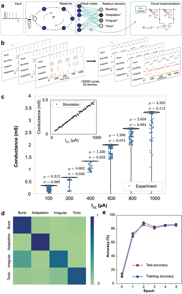
### Visual Description
## Diagram: Reservoir Computing System Performance
### Overview
The image presents a multi-panel diagram illustrating a reservoir computing system, its implementation, and performance characteristics. Panel (a) shows a schematic of the reservoir computing architecture. Panel (b) displays raster plots of neuron activity for different neuron types. Panel (c) presents a scatter plot comparing simulated and experimental conductance data. Panel (d) shows a heatmap of neuron type distribution and a graph of training/testing accuracy over epochs.
### Components/Axes
**Panel a:**
* **Labels:** Input, Reservoir, Virtual nodes, Readout neurons, Circuit implementation, Icc Control, G*, G.
* **Diagram Elements:** Input signal flowing into a reservoir of interconnected neurons, readout layer connecting the reservoir to output neurons, and a circuit implementation showing transistors.
* **Annotations:** τ (time constant), W<sub>ij</sub> (weights).
**Panel b:**
* **Labels:** Bursting, Adaptation, Irregular, Tonic, Time (ms).
* **Axes:** X-axis: Time (0-1000 ms). Y-axis: Neuron index (25 devices).
* **Legend:** Bursting (orange), Adaptation (purple), Irregular (blue), Tonic (green).
**Panel c:**
* **Labels:** Conductance (mS), I<sub>cc</sub> (µA), Simulation, Experiment.
* **Axes:** X-axis: I<sub>cc</sub> (µA) (0-1100). Y-axis: Conductance (mS) (0-4).
* **Annotations:** μ (mean), σ (standard deviation) values for simulation and experiment.
* **Inset:** A smaller scatter plot showing simulation data.
**Panel d:**
* **Labels:** Burst, Adaptation, Irregular, Tonic, Epoch.
* **Heatmap Axes:** X-axis: Neuron type (Burst, Adaptation, Irregular, Tonic). Y-axis: Neuron type (Burst, Adaptation, Irregular, Tonic).
* **Accuracy Graph Axes:** X-axis: Epoch (1-5). Y-axis: Accuracy (%) (0-100).
* **Legend:** Test accuracy (black), Training accuracy (red).
### Detailed Analysis or Content Details
**Panel a:**
The diagram illustrates a reservoir computing system. An input signal is fed into a reservoir of randomly connected neurons. The reservoir's state is then mapped to output neurons via a readout layer. The circuit implementation shows a transistor-based circuit with Icc control and gate voltages G* and G.
**Panel b:**
Raster plots show the spiking activity of different neuron types over time. The plots display 25 devices.
* **Bursting:** Shows sporadic, high-frequency bursts of activity.
* **Adaptation:** Shows activity that adapts over time, decreasing in frequency.
* **Irregular:** Shows a relatively constant, random spiking pattern.
* **Tonic:** Shows a consistent, low-frequency spiking pattern.
**Panel c:**
A scatter plot compares simulated and experimental conductance data as a function of I<sub>cc</sub>.
* **Simulation:** The simulation data shows a positive correlation between conductance and I<sub>cc</sub>. The mean (μ) is approximately 0.312 mS, with a standard deviation (σ) of approximately 0.060 mS.
* **Experiment:** The experimental data also shows a positive correlation, but with a wider spread. The mean (μ) is approximately 1.330 mS, with a standard deviation (σ) of approximately 0.033 mS.
* **Inset:** The inset shows a zoomed-in view of the simulation data, revealing a more detailed relationship between conductance and I<sub>cc</sub>.
* **Overall:** The experimental data has a higher conductance range than the simulation data. The mean (μ) for the experiment is approximately 2.658 mS, with a standard deviation (σ) of approximately 0.084 mS. The mean (μ) for the experiment is approximately 3.325 mS, with a standard deviation (σ) of approximately 0.112 mS.
**Panel d:**
* **Heatmap:** The heatmap shows the distribution of neuron types. The diagonal elements (Burst-Burst, Adaptation-Adaptation, etc.) are the most prominent, indicating a higher proportion of neurons of the same type.
* **Accuracy Graph:** The graph shows the training and testing accuracy of the reservoir computing system over epochs.
* **Training Accuracy:** Starts at approximately 20% at epoch 1 and increases to approximately 80% by epoch 5.
* **Test Accuracy:** Starts at approximately 40% at epoch 1 and plateaus at approximately 70% by epoch 3, remaining relatively stable through epoch 5.
### Key Observations
* The experimental conductance values are significantly higher than the simulated values.
* The accuracy graph shows a clear overfitting trend, with training accuracy increasing while test accuracy plateaus.
* The heatmap suggests a preference for neurons of the same type within the reservoir.
* The raster plots in panel (b) clearly differentiate the spiking behavior of the four neuron types.
### Interpretation
The diagram demonstrates the implementation and performance of a reservoir computing system. The comparison between simulation and experiment highlights the discrepancies between theoretical models and real-world implementations, potentially due to factors not captured in the simulation. The accuracy graph reveals a potential overfitting issue, suggesting that the model is memorizing the training data rather than generalizing to unseen data. The heatmap provides insight into the composition of the reservoir, indicating a non-uniform distribution of neuron types. The different spiking patterns observed in the raster plots suggest that the neuron types contribute differently to the reservoir's dynamics. The overall system demonstrates the potential of reservoir computing for complex information processing, but also highlights the challenges of bridging the gap between simulation and experiment and avoiding overfitting. The Icc control and transistor-based circuit implementation in panel (a) suggest a physical realization of the reservoir computing concept. The data suggests that the system is capable of learning, but requires careful tuning to avoid overfitting and achieve optimal performance.
</details>
## MOSAIC: AN ANALOG SYSTOLIC ARCHITECTURE FOR IN-MEMORY COMPUTING AND ROUTING
This chapter's content was published in Nature Communications, featured as one of 50 best papers recently published in the field. The original publication is authored by Yigit Demirag ∗ , Thomas Dalgaty ∗ , Filippo Moro ∗ , Alessio De Pra, Giacomo Indiveri, Elisa Vianello and Melika Payvand.
∗ These authors contributed equally.
The brain's connectivity is locally dense and globally sparse, forming a small-world graph-a principle prevalent in the evolution of various species, suggesting a universal solution for efficient information routing. However, current artificial neural network circuit architectures do not fully embrace small-world neural network models. Here, we present the neuromorphic Mosaic: a nonvon Neumann systolic architecture employing distributed memristors for in-memory computing and in-memory routing, efficiently implementing small-world graph topologies for SNNs. We've designed, fabricated, and experimentally demonstrated the Mosaic's building blocks, using integrated memristors with 130 nm CMOS technology. We show that thanks to enforcing locality in the connectivity, routing efficiency of Mosaic is at least one order of magnitude higher than other SNN hardware platforms. This is while Mosaic achieves a competitive accuracy in a variety of edge benchmarks. Mosaic offers a scalable approach for edge systems based on distributed spike-based computing and in-memory routing.
## 5 . 1 introduction
Despite millions of years of evolution, the fundamental wiring principle of biological brains has been preserved: dense local and sparse global connectivity through synapses between neurons. This persistence indicates the efficiency of this solution in optimizing both computation and the utilization of the underlying neural substrate [ 30 ]. Studies have revealed that this connectivity pattern in neuronal networks increases the signal propagation speed [ 279 ], enhances echo-state properties [ 280 ] and allows for a more synchronized global network [ 281 ]. While densely connected neurons in the network are attributed to performing functions such as integration and feature extraction functions [ 282 ], long-range sparse connections may play a significant role in the hierarchical organization of such functions [ 283 ]. Such neural connectivity is called smallworldness in graph theory and is widely observed in the cortical connections of the human brain [ 279 , 284 , 285 ] (Fig. 5 . 1 a, b). Small-world connectivity matrices, representing neuronal connections, display a distinctive pattern with a dense diagonal and progressively fewer connections between neurons as their distance from the diagonal increases (see Fig. 5 . 1 c).
Crossbar arrays of non-volatile memory technologies e.g., Floating Gates [ 287 ], RRAM [ 139 , 191 , 288 -291 ], and PCM [ 138 , 292 -294 ] have been previously proposed as a means for realizing artificial neural networks on hardware (Fig. 5 . 1 d). These computing architectures perform in-memory vector-matrix multiplication, the core operation of artificial neural networks, reducing the data movement, and consequently the power consumption, relative to conventional von Neumann architectures [ 144 , 287 , 295 -299 ].
However, existing crossbar array architectures are not inherently efficient for realizing smallworld neural networks at all scales. Implementing networks with small-world connectivity in a large crossbar array would result in an under-utilization of the off-diagonal memory elements (i.e., a ratio of non-allocated to allocated connections > 10) (see Fig. 5 . 1 d and Supplementary Note 1 ). Furthermore, the impact of analog-related hardware non-idealities such as current sneak-paths, parasitic resistance, and capacitance of the metal lines, as well as excessively large read currents and diminishing yield limit the maximum size of crossbar arrays in practice [ 99 -101 ].
These issues are also common to biological networks. As the resistance attenuates the spread of the action potential, cytoplasmic resistance sets an upper bound to the length of dendrites [ 30 ].
F igure 5 . 1 : Small-world graphs in biological network and how to build that into a hardware architecture for edge applications . (a) Depiction of small-world property in the brain, with highly-clustered neighboring regions highlighted with the same color. (b) Network connectivity of the brain is a small-world graph, with highly clustered groups of neurons with sparse connectivity among them. (c) (adapted from Bullmore and Sporns 2009 [ 286 ]). The functional connectivity matrix which is derived from anatomical data with rows and columns representing neural units. The diagonal region of the matrix (darkest colors) contains the strongest connectivity which represents the connections between the neighboring regions. The off-diagonal elements are not connected. (d) Hardware implementation of the connectivity matrix of c, with neurons and synapses arranged in a crossbar architecture. The red squares represent the group of memory devices in the diagonal, connecting neighboring neurons. Black squares show the group of memory devices that are never programmed in a small-world network, and are thus highlighted as 'wasted'. (e) The Mosaic architecture breaks the large crossbars into small densely-connected crossbars (green Neuron Tiles) and connects them through small routing crossbars (blue Routing Tiles). This gives rise to a distributed two-dimensional mesh, with highly connected clusters of neurons, connected to each other through routers. (f) The state of the resistive memory devices in Neuron Tiles determines how the information is processed, while the state of the routing devices determines how it is propagated in the mesh. The resistive memory devices are integrated into 130 nm technology. (g) Plot showing the required memory (number of memristors) as a function of the number of neurons per tile, for different total numbers of neurons in the network. The horizontal dashed line indicates the number of required memory bits using a fully-connected RRAM crossbar array. The cross (X) illustrates the cross-over point below which the Mosaic approach becomes favorable. (h) The Mosaic can be used for a variety of edge AI applications, benchmarked here on sensory processing and Reinforcement learning tasks.
<details>
<summary>Image 32 Details</summary>
### Visual Description
\n
## Diagram: Neuromorphic Computing Architecture
### Overview
This diagram illustrates a neuromorphic computing architecture, focusing on a small-world network implementation on memory crossbars and a mosaic layout optimized for routing and computing. It showcases the transition from a complex network to a simplified representation, the structure of memory units, and the application of this architecture to various tasks.
### Components/Axes
The diagram is segmented into several parts:
* **(a)**: A complex, colorful network representation.
* **(b)**: A simplified network representation with nodes and connections. A circle highlights a specific region.
* **(c)**: A scatter plot showing neural unit activity. X-axis labeled "Neural unit", Y-axis labeled "Neural unit".
* **(d)**: A grid representing a memory unit, with "High G memory unit" (red squares) and "Low G memory unit" (black squares). Labeled "Input" points to the top row. "Wasted" is labeled at the bottom right.
* **(e)**: A mosaic layout of interconnected tiles.
* **(f)**: A schematic showing connections between tiles and memory units, with a symbol resembling a resistor (Ω) in the center.
* **(g)**: A log-log plot of "# Memory elements" vs. "# Neurons per neuron tile". X-axis ranges from 2 to 64. Y-axis ranges from 10^0 to 10^6.
* **(h)**: Illustrations of applications: Continuous space reinforcement learning, Keyword Spotting, and Anomaly detection.
* **Footer**: Text describing the architecture: "Under-utilized small-world implementation on memory crossbars" and "Mosaic: Small-world optimized layout for routing and computing".
### Detailed Analysis or Content Details
**Part (a) & (b): Network Simplification**
Part (a) shows a highly interconnected network with nodes colored in various shades (red, green, blue, purple). Part (b) presents a simplified view of the same network, with nodes represented as dots (purple and green) and connections as lines. The highlighted circle in (b) suggests a focus on a specific sub-network.
**Part (c): Neural Unit Activity**
This is a scatter plot showing the activity of neural units. The plot appears to have a sparse distribution of points, indicating that not all neural units are active simultaneously. The density of points is relatively low.
**Part (d): Memory Unit Structure**
The grid represents a memory unit. Red squares denote "High G memory unit", while black squares denote "Low G memory unit". The "Input" is at the top. The bottom right corner is labeled "Wasted", suggesting unused memory space. The grid is approximately 10x10.
**Part (e): Mosaic Layout**
This shows a grid of interconnected tiles. Each tile contains a smaller grid of units. The tiles are connected, forming a larger network.
**Part (f): Tile Connections**
This schematic illustrates how tiles are connected to memory units. The resistor symbol (Ω) likely represents a weighting or resistance value in the circuit. The connections appear to be bidirectional.
**Part (g): Memory Elements vs. Neurons**
This log-log plot shows the relationship between the number of memory elements and the number of neurons per neuron tile. There are five lines representing different numbers of neurons: 128 (dark green), 256 (blue), 512 (light green), 1024 (red), and a dashed line representing a theoretical limit.
* **128 Neurons (Dark Green):** Starts at approximately 10^3 memory elements at 2 neurons/tile, and rises to approximately 2x10^5 memory elements at 64 neurons/tile.
* **256 Neurons (Blue):** Starts at approximately 2x10^3 memory elements at 2 neurons/tile, and rises to approximately 4x10^5 memory elements at 64 neurons/tile.
* **512 Neurons (Light Green):** Starts at approximately 4x10^3 memory elements at 2 neurons/tile, and rises to approximately 8x10^5 memory elements at 64 neurons/tile.
* **1024 Neurons (Red):** Starts at approximately 8x10^3 memory elements at 2 neurons/tile, and rises to approximately 1.6x10^6 memory elements at 64 neurons/tile.
* **Dashed Line:** Represents a theoretical upper bound, starting at approximately 1x10^3 memory elements at 2 neurons/tile, and rising to approximately 1x10^6 memory elements at 64 neurons/tile.
All lines exhibit a positive slope, indicating that the number of memory elements increases with the number of neurons per tile. The lines are roughly parallel, suggesting a linear relationship.
**Part (h): Applications**
This section demonstrates the application of the architecture to three tasks:
* **Continuous space reinforcement learning:** Shown with a waveform.
* **Keyword Spotting:** Shown with a waveform.
* **Anomaly detection:** Shown with a waveform.
A small image of a chip is also shown with an arrow pointing to "Wide application range".
### Key Observations
* The architecture leverages a small-world network for efficient routing and computation.
* The memory unit structure utilizes both high and low conductance memory units.
* The number of memory elements scales with the number of neurons per tile, but there appears to be a limit to this scaling.
* The architecture is versatile and can be applied to various machine learning tasks.
### Interpretation
The diagram presents a novel neuromorphic computing architecture that aims to overcome the limitations of traditional von Neumann architectures. The small-world network implementation on memory crossbars provides efficient routing and computation, while the mosaic layout allows for scalability. The use of both high and low conductance memory units enables more complex computations. The log-log plot (g) suggests a trade-off between the number of memory elements and the number of neurons per tile, indicating that there is a limit to how densely the network can be packed. The applications shown in (h) demonstrate the potential of this architecture for a wide range of machine learning tasks. The "Wasted" label in (d) suggests that there is room for optimization in the memory unit design. The overall design appears to be focused on energy efficiency and parallel processing, which are key advantages of neuromorphic computing.
</details>
Hence, the intrinsic physical structure of the nervous systems necessitates the use of local over global connectivity.
Drawing inspiration from the biological solution for the same problem leads to (i) a similar optimal silicon layout, a small-world graph, and (ii) a similar information transfer mechanism through electrical pulses, or spikes. A large crossbar can be divided into an array of smaller, more locally connected crossbars. These correspond to the green squares of Fig. 5 . 1 e. Each green crossbar hosts a cluster of spiking neurons with a high degree of local connectivity. To pass information among these clusters, small routers can be placed between them - the blue tiles in Fig. 5 . 1 e. We call this two-dimensional systolic matrix of distributed crossbars, or tiles, the neuromorphic Mosaic architecture. Each green tile serves as an analog computing core, which sends out information in the form of spikes, while each blue tile serves as a routing core that spreads the spikes throughout the mesh to other green tiles. Thus, the Mosaic takes advantage of distributed and de-centralized computing and routing to enable not only in-memory computing, but also in-memory routing (Fig. 5 . 1 f). Though the Mosaic architecture is independent of the choice of memory technology, here we are taking advantage of the resistive memory, for its non-volatility, small footprint, low access time and power, and fast programming [ 300 ].
Neighborhood-based computing with resistive memory has been previously explored through using Cellular Neural Networks [ 301 , 302 ], Self-organizing Maps (SOM) [ 303 ], and the crossnet architecture [ 304 ]. Though cellular architectures use local clustering, their lack of global connectivity limits both the speed of information propagation and their configurability. Therefore their application has been mostly limited to low-level image processing [ 305 ]. This also applies for SOMs, which exploit neighboring connectivity and are typically trained with unsupervised methods to visualize low-dimensional data [ 306 ]. Similarly, the crossnet architecture proposed to use distributed small tilted integrated crossbars on top of the CMOS substrate, to create local connectivity domains for image processing [ 304 ]. The tilted crossbars allow the nano-wire feature size to be independent of the CMOS technology node [ 307 ]. However, this approach requires extra post-processing lithographic steps in the fabrication process, which has so far limited its realization.
Unlike most previous approaches, the Mosaic supports both dense local connectivity, and globally sparse long-range connections, by introducing re-configurable routing crossbars between the computing tiles. This allows to flexibly program specific small-world network configurations and to compile them onto the Mosaic for solving the desired task. Moreover, the Mosaic is fully compatible with standard integrated RRAM/CMOS processes available at the foundries, without the need for extra post-processing steps. Specifically, we have designed the Mosaic for smallworld SNNs, where the communication between the tiles is through electrical pulses, or spikes. In the realm of SNN hardware, the Mosaic goes beyond the AER [ 103 , 308 , 309 ], the standard spike-based communication scheme, by removing the need to store each neuron's connectivity information in either bulky local or centralized memory units which draw static power and can consume a large chip area (Supplementary Note 2 ).
In this Article, we first present the Mosaic architecture. We report electrical circuit measurements from computational and Routing Tiles that we designed and fabricated in 130 nm CMOS technology co-integrated with Hafnium dioxide-based RRAM devices. Then, calibrated on these measurements, and using a novel method for training small-world neural networks that exploits the intrinsic layout of the Mosaic, we run system-level simulations applied to a variety of edge computing tasks (Fig. 5 . 1 h). Finally, we compare our approach to other neuromorphic hardware platforms which highlights the significant reduction in spike-routing energy, between one and four orders of magnitude.
## 5 . 2 mosaic hardware computing and routing measurements
In the Mosaic (Fig. 5 . 1 e), each of the tiles consists of a small memristor crossbar that can receive and transmit spikes to and from their neighboring tiles to the North (N), South (S), East (E) and West (W) directions (Supplementary Note 4 ). The memristive crossbar array in the green Neuron Tiles stores the synaptic weights of several LIF neurons. These neurons are implemented using
analog circuits and are located at the termination of each row, emitting voltage spikes at their outputs [ 29 ]. The spikes from the Neuron Tile are copied in four directions of N, S, E and W. These spikes are communicated between Neuron Tiles through a mesh of blue Routing Tiles, whose crossbar array stores the connectivity pattern between Neuron Tiles. The Routing Tiles at different directions decides whether or not the received spike should be further communicated. Together, the two tiles give rise to a continuous mosaic of neuromorphic computation and memory for realizing small-world SNNs.
Small-world topology can be obtained by randomly programming memristors in a computer model of the Mosaic (see Methods and Supplementary Note 3 ). The resulting graph exhibits an intriguing set of connection patterns that reflect those found in many of the small-world graphical motifs observed in animal nervous systems. For example, central 'hub-like' neurons with connections to numerous nodes, reciprocal connections between pairs of nodes reminiscent of winner-take-all mechanisms, and some heavily connected local neural clusters [ 285 ]. If desired, these graph properties could be adapted on the fly by re-programming the RRAM states in the two tile types. For example, a set of desired small-world graph properties can be achieved by randomly programming the RRAM devices into their HCS with a certain probability (Supplementary Note 3 ). Random programming can for example be achieved elegantly by simply modulating RRAM programming voltages [ 125 ].
For Mosaic-based small-world graphs, we estimate the required number of memory devices (synaptic weight and routing weight) as a function of the total number of neurons in a network, through a mathematical derivation (see Methods). Fig. 5 . 1 g plots the memory footprint as a function of the number of neurons in each tile for different network sizes. Horizontal dashed lines show the number of memory elements using one large crossbar for each network size, as has previously been used for RNN implementations [ 310 ]. The cross-over points, at which the Mosaic memory footprint becomes favorable, are denoted with a cross. While for smaller network sizes (i.e. 128 neurons) no memory reduction is observed compared to a single large array, the memory saving becomes increasingly important as the network is scaled. For example, given a network of 1024 neurons and 4 neurons per Neuron Tile, the Mosaic requires almost one order of magnitude fewer memory devices than a single crossbar to implement an equivalent network model.
neuron tile circuits : small -worlds Each Neuron Tile in the Mosaic (Fig. 5 . 2 a) is composed of multiple rows, a circuit that models a LIF neuron and its synapses. The details of one neuron row is shown in Fig. 5 . 2 b. It has N parallel one-transistor-one-resistor ( 1 T 1 R) RRAM structures at its input. The synaptic weights of each neuron are stored in the conductance level of the RRAM devices in one row. On the arrival of any of the input events Vin < i > , the amplifier pins node Vx to Vtop , and thus a read voltage equivalent to Vtop -Vbot is applied across Gi , giving rise to current i in at M 1 , and in turn to i buf f . This current pulse is mirrored through Iw to the 'synaptic dynamics' circuit, Differential Pair Integrator (DPI) [ 311 ], which low pass filters it through charging the capacitor M 9 in the presence of the pulse, and discharging it through current Itau in its absence. The charge/discharge of M 9 generates an exponentially decaying current, Isyn , which is injected into the neuron's membrane potential node, Vmem , and charges capacitor M 13 . The capacitor leaks through M 11 , whose rate is controlled by Vlk at its gate. As soon as the voltage developed on Vmem passes the threshold of the following inverter stage, it generates a pulse, at Vout . The refractory period time constant depends on the capacitor M 16 and the bias on Vrp . (For a more detailed explanation of the circuit, please see Supplementary Note 5 ).
We have fabricated and measured the circuits of the Neuron Tile in a 130 nm CMOS technology integrated with RRAM devices [ 119 ]. The measurements were done on the wafer level, using a probe station shown in Fig. 5 . 2 c. In the fabricated circuit, we statistically characterized the RRAMs through iterative programming [ 312 ] and controlling the programming current, resulting in nine stable conductance states, G , shown in Fig. 5 . 2 d. After programming each device, we apply a pulse on Vin < 0 > and measure the voltage on Vsyn , which is the voltage developed on the M 9 capacitor. We repeat the experiment for four different conductance levels of 4 µ S , 48 µ S , 64 µ S and 147 µ S . The resulting Vsyn traces are plotted in Fig. 5 . 2 e. Vsyn starts from the initial value close to the power supply, 1 . 2 V. The amount of discharge depends on the Iw current which is a linear function of the conductance value of the RRAM, G . The higher the G , the higher the
x
i
t
o
p
i
w
F igure 5 . 2 : Experimental results from the neuron column circuit. (a) Neuron Tile, a crossbar with feed-forward and recurrent inputs displaying network parameters represented by colored squares. (b) Schematic of a single row of the fabricated crossbars, where RRAMs represent neuron weights. Insets show scanning and transmission electron microscopy images of the 1 T 1 R stack with a hafnium-dioxide layer sandwiched between memristor electrodes. Upon input events Vin < i > , Vtop -Vbot is applied across Gi , yielding i in and subsequently i buf f , which feeds into the synaptic dynamic block, producing exponentially decaying current isyn , with a time constant set by MOS capacitor M 9 and bias current Itau . Integration of isyn into neuron membrane potential Vmem triggers an output pulse ( Vout ) upon exceeding the inverter threshold. Refractory period regulation is achieved through MOS cap M 16 and Vrp bias. (c) Wafer-level measurement setup utilizes an Arduino for logic circuitry management to program RRAMs and a B 1500 Device Parameter Analyzer to read device conductance. (d) Cumulative distributions of RRAM conductance ( G ) resulting from iterative programming in a 4096 -device RRAM array with varied SET programming currents. (e) Vsyn initially at 1 . 2 ,V decreases as capacitor M 9 discharges upon pulse arrival at time 0 . Discharge magnitude depends on Iw set by G . Four conductance values' Vsyn curves are recorded. (f) Input pulse train (gray pulses) at Vin < 0 > increases zeroth neuron's Vmem (purple trace) until it fires (light blue trace) after six pulses, causing feedback influence on neuron 1 's Vmem . (g) Statistical measurements on peak membrane potential in response to a pulse across a 5 -neuron array over 10 cycles. (h) Neuron output frequency linearly correlates with G , with error bars reflecting variability across 4096 devices.
<details>
<summary>Image 33 Details</summary>
### Visual Description
## Circuit Diagram & Performance Characterization: Neuromorphic Computing System
### Overview
The image presents a combination of a circuit diagram, experimental setup photograph, and performance characterization graphs related to a neuromorphic computing system. The system appears to be based on resistive random-access memory (RRAM) and utilizes a chain of inverters to implement neuron and synapse functionality. The image details the circuit architecture, experimental setup, and the relationship between RRAM conductance and the resulting output frequency.
### Components/Axes
The image is divided into several sub-sections:
* **(a):** Chain of inverters representing a neuron circuit.
* **(b):** Detailed schematic of the neuron circuit with RRAM elements.
* **(c):** Photograph of the experimental setup, including hardware and monitoring equipment.
* **(d):** Cumulative Distribution Function (CDF) of RRAM conductance (G). X-axis: G (µs), Y-axis: CDF (0.00 - 1.00).
* **(e):** Simulation of input voltage (V<sub>in</sub>) over time for different RRAM conductance values. X-axis: Time (ms), Y-axis: V<sub>in</sub> (V).
* **(f):** Voltage waveform showing the output of the inverter chain for different input voltages. X-axis: Time (ms), Y-axis: Voltage (V).
* **(g):** Box plot of peak output voltage (V<sub>peak</sub>) for different neuron row IDs. X-axis: Neuron Row ID (1-5), Y-axis: V<sub>peak</sub> (V).
* **(h):** Output frequency versus RRAM conductance. X-axis: RRAM Conductance (µs), Y-axis: Output Frequency (kHz). Two lines are shown for different input voltages (V<sub>in</sub> = 250mV and V<sub>in</sub> = 300mV).
### Detailed Analysis or Content Details
**(a) Inverter Chain:**
A series of inverters are shown, with input signals propagating from left to right. The input signal is a square wave.
**(b) Neuron Circuit Schematic:**
The schematic shows transistors (M1, M2, M3, etc.) and RRAM devices. The RRAM devices are labeled with conductance values (G). The schematic includes voltage sources (V<sub>in</sub>, V<sub>dd</sub>, V<sub>ss</sub>) and an output (V<sub>out</sub>).
**(c) Experimental Setup:**
The photograph shows a rack of electronic equipment, including a computer monitor displaying waveforms, and a circuit board with the neuromorphic chip.
**(d) CDF of RRAM Conductance:**
The CDF shows the distribution of RRAM conductance values. Multiple curves are plotted, each representing a different RRAM device. The conductance values range from approximately 25 µs to 125 µs. The CDF indicates that the conductance values are not uniformly distributed.
**(e) Input Voltage Simulation:**
The graph shows the simulated input voltage (V<sub>in</sub>) over time for different RRAM conductance values (G = 147 µs, 64 µs, 48 µs, 4 µs). The curves show that higher conductance values result in faster voltage transitions. The Y-axis ranges from approximately 0.9V to 1.2V. The X-axis ranges from 0.0 to 0.25 ms.
**(f) Voltage Waveform:**
The graph shows the output voltage waveform for different input voltages (V<sub><0</sub>, V<sub><1</sub>, V<sub><2</sub>, V<sub><3</sub>). The waveform shows a delayed and inverted signal. The Y-axis ranges from 0.0 to 1.0V. The X-axis ranges from 0.0 to 1.2 ms.
**(g) Peak Output Voltage:**
The box plot shows the distribution of peak output voltages (V<sub>peak</sub>) for different neuron row IDs (1-5). Neuron row ID 4 has the highest median V<sub>peak</sub>, approximately 0.35V. Neuron row ID 1 has the lowest median V<sub>peak</sub>, approximately 0.15V. The Y-axis ranges from 0.0 to 0.4V.
**(h) Output Frequency vs. Conductance:**
The graph shows the relationship between output frequency and RRAM conductance for two different input voltages (V<sub>in</sub> = 250mV and V<sub>in</sub> = 300mV). Both lines show an upward trend, indicating that higher conductance values result in higher output frequencies. The line for V<sub>in</sub> = 300mV is consistently above the line for V<sub>in</sub> = 250mV. At a conductance of 40 µs, the output frequency is approximately 10 kHz for V<sub>in</sub> = 250mV and approximately 20 kHz for V<sub>in</sub> = 300mV. At a conductance of 120 µs, the output frequency is approximately 60 kHz for V<sub>in</sub> = 250mV and approximately 80 kHz for V<sub>in</sub> = 300mV.
### Key Observations
* The CDF of RRAM conductance (d) shows a non-uniform distribution, suggesting variability in the RRAM devices.
* Higher RRAM conductance values lead to faster voltage transitions in the simulation (e).
* The output frequency increases with RRAM conductance (h), demonstrating the synaptic weight effect.
* Neuron row ID 4 exhibits the highest peak output voltage (g).
* Increasing the input voltage (V<sub>in</sub>) increases the output frequency (h).
### Interpretation
The image demonstrates a neuromorphic computing system based on RRAM synapses and inverter-based neurons. The RRAM conductance acts as a synaptic weight, modulating the output frequency of the neuron. The simulation and experimental results confirm that higher conductance values lead to higher output frequencies, mimicking the behavior of biological synapses. The variability in RRAM conductance, as shown by the CDF, could impact the performance and reliability of the system. The differences in peak output voltage between neuron rows suggest variations in device characteristics or circuit layout. The system's ability to modulate output frequency based on conductance provides a foundation for implementing complex neural networks. The experimental setup photograph provides context for the research and development of this neuromorphic system. The data suggests a functional neuromorphic system, but further characterization and optimization are needed to address the variability in RRAM devices and improve overall performance.
</details>
Iw , and higher the decrease in Vsyn , resulting in higher Isyn which is integrated by the neuron membrane Vmem . The peak value of the membrane potential in response to a pulse is measured across one array of 5 neurons, each with a different conductance level (Fig. 5 . 2 g). Each pulse increases the membrane potential according to the corresponding conductance level, and once it hits a threshold, it generates an output spike (Fig. 5 . 2 f). The peak value of the neuron's membrane potential and thus its firing rate is proportional to the conductance G , as shown in Fig. 5 . 2 h. The error bars on the plot show the variability of the devices in the 4 kb array. It is worth noting that this implementation does not take into account the negative weight, as the focus of the design has been on the concept. Negative weights could be implemented using a differential signaling approach, by using two RRAMs per synapse [ 115 ].
routing tile circuits : connecting small -worlds A Routing Tile circuit is shown in Fig. 5 . 3 a. It acts as a flexible means of configuring how spikes emitted from Neuron Tiles propagate locally between small-worlds. Thus, the routed message entails a spike, which is either
w
l
k
r
p
F igure 5 . 3 : Experimental measurements of the fabricated Routing Tile circuits. (a) The Routing Tile, a crossbar whose memory state steers the input spikes from different directions towards the destination. (b) Detailed schematic of one row of the fabricated routing circuits. On the arrival of a spike to any of the input ports of the Routing Tile, V in < i > , a current proportional to Gi flows in i in , similar to the Neuron Tile. A current comparator compares this current against a reference current, I re f , which is a bias current generated on chip through providing a DC voltage from the I/O pads to the gate of an on-chip transistor. If i in > i re f , the spike will get regenerated, thus 'pass', or is 'blocked' otherwise. (c) Wafer-level measurements of the test circuits through the probe station test setup. (d) Measurements from 4 kb array shows the Cumulative Distribution Function (CDF) of the RRAM in its High Conductive State (HCS) and Low Conductive State (LCS). The line between the distributions that separates the two is considered as the 'Threshold' conductance, which the decision boundary for passing or blocking the spikes. Based on this Threshold value, the I re f bias in panel (b) is determined. (e) Experimental results from the Routing Tile, with continuous and dashed blue traces showing the waveforms applied to the <N> and <S> inputs, while the orange trace shows the response of the output towards the <E> port. The <E> output port follows the <N> input, resulting from the device programmed into the HCS, while the input from the <S> port gets blocked as the corresponding RRAM device is in its LCS. (f) A binary checker-board pattern is programmed into the routing array, to show a ratio of 10 between the High Resistive and Low Resistive state, which sets a perfect boundary for a binary decision required for the Routing Tile.
<details>
<summary>Image 34 Details</summary>
### Visual Description
## Diagram Set: Neuromorphic Computing Components & Characteristics
### Overview
This image presents a set of diagrams and data visualizations related to neuromorphic computing, specifically focusing on memristive devices and their application in building logic gates and neural networks. The image is divided into six sections (a-f), each illustrating a different aspect of the system.
### Components/Axes
* **a:** Schematic representation of a memristive crossbar array with labeled inputs: <N>, <W>, <S>, <E>.
* **b:** Circuit diagram showing the implementation of a logic gate using memristors and an operational amplifier. Includes transistor schematics and voltage labels (V<sub>bot</sub>, V<sub>in</sub>, V<sub>buff</sub>, V<sub>out</sub>).
* **c:** Photograph of a physical experimental setup, likely a probe station with a memristive device under test.
* **d:** Cumulative Distribution Function (CDF) plot of conductance (µS) with labeled curves: LCS (Low Conductance State) and HCS (High Conductance State). X-axis: Conductance (µS) from 0 to 125. Y-axis: CDF from 0 to 1.0. A vertical line indicates a "Threshold" value at approximately 25 µS.
* **e:** Time-series plot of voltage (V<sub>in</sub>) vs. time (µs) for different input signals: V<sub>in</sub> <N>, V<sub>in</sub> <W>, V<sub>in</sub> <S>, V<sub>in</sub> <E>. X-axis: Time (µs) from -4 to 8. Y-axis: Voltage (V) from 0 to 1.2.
* **f:** Heatmap showing conductance (µS) as a function of inputs (0, 1, 2, 3) and outputs. X-axis: Inputs (0, 1, 2, 3). Y-axis: Conductance (µS) from 20 to 80.
### Detailed Analysis or Content Details
**a:** The schematic shows a grid of square elements, presumably memristors, arranged in a crossbar configuration. The inputs <N>, <W>, <S>, and <E> likely represent North, West, South, and East, indicating the direction of addressing or signal input.
**b:** The circuit diagram illustrates a differential amplifier configuration. The memristors (labeled G<sub>i</sub>) are connected in series between the input and output. The transistors are arranged in a cascaded inverter configuration. The diagram shows how the memristor's conductance modulates the output voltage.
**c:** The photograph shows a complex experimental setup with various cables and components. It appears to be a probe station used for making electrical contact with a small device.
**d:** The CDF plot shows the distribution of conductance values for the memristive devices. The LCS curve rises steeply from 0 to approximately 0.4 at around 10 µS, indicating a high probability of low conductance states. The HCS curve rises more gradually, reaching 0.4 at around 50 µS, indicating a broader distribution of high conductance states. The threshold is set at approximately 25 µS.
**e:** The time-series plot shows voltage pulses for each input signal. The pulses are approximately 2 µs wide and have a peak voltage of around 1.2 V. The pulses are offset in time, suggesting sequential application of inputs.
**f:** The heatmap shows the relationship between inputs and conductance. The color intensity represents the conductance value. The heatmap appears to demonstrate a non-linear relationship between inputs and outputs, with varying conductance values for different input combinations. The conductance values range from approximately 20 µS to 80 µS. The pattern suggests a complex mapping between inputs and outputs, potentially representing a logic function or a neural network weight matrix.
### Key Observations
* The CDF plot (d) shows a clear bimodal distribution of conductance, indicating distinct low and high conductance states.
* The time-series plot (e) demonstrates the ability to apply different input signals sequentially.
* The heatmap (f) suggests a complex, non-linear relationship between inputs and outputs, indicative of computational functionality.
* The circuit diagram (b) shows a potential implementation of a logic gate using memristors.
### Interpretation
The image demonstrates the potential of memristive devices for building neuromorphic computing systems. The crossbar array (a) provides a dense connectivity matrix, while the circuit diagram (b) shows how memristors can be used to implement logic gates. The CDF plot (d) confirms the bistable nature of the memristors, allowing them to store information in the form of conductance states. The time-series plot (e) shows the ability to control the input signals, and the heatmap (f) suggests that the system can perform complex computations.
The threshold value in the CDF plot (d) is crucial for defining the switching behavior of the memristors. The non-linear relationship between inputs and outputs in the heatmap (f) is a key characteristic of neural networks and other complex computational systems. The experimental setup in (c) suggests that these concepts are being actively investigated in a laboratory setting.
The overall data suggests a functional neuromorphic system capable of performing computations based on the manipulation of memristive conductance states. The system's ability to represent and process information in a manner analogous to the human brain could lead to significant advances in artificial intelligence and machine learning.
</details>
blocked by the router, if the corresponding RRAM is in its HRS, or is passed otherwise. The functional principles of the Routing Tile circuits are similar to the Neuron Tiles. The principal difference is the replacement of the synapse and neuron circuit models with a simple current comparator circuit (highlighted with a black box in Fig. 5 . 3 b). The measurements were done on the wafer level, using a probe station shown in Fig. 5 . 3 c. On the arrival of a spike on an input port of the Routing Tile, V in < i > , 0 < i < N , a current proportional to Gi flows to the device, giving rise to read current i buf f . A current comparator compares i buf f against i re f , which is a bias generated on chip by providing a voltage from the I/O pad to the gate of a transistor (not shown in the Fig.). The I re f value is decided based on the 'Threshold' conductance boundary in Fig. 5 . 3 d. The Routing Tile regenerates a spike if the resulting i buf f is higher than i re f , and blocks it otherwise, since the output remains at zero. Therefore, the state of the device serves to either pass or block input spikes arriving from different input ports ( N , S , W , E ), sending them to its output ports (Supplementary Note 4 ). Since the routing array acts as a binary pass or no-pass, the decision boundary is on whether the devices is in its HCS or LCS, as shown in Fig. 5 . 3 d [ 313 ]. Using a fabricated Routing Tile circuit, we demonstrate its functionality experimentally in Fig. 5 . 3 e. Continuous and dashed blue traces show the waveforms applied to the <N> and <S> inputs of the tile respectively, while the orange trace shows the response of the output towards the E port. The E output port follows the N input resulting from the corresponding RRAM programmed into its HCS, while the input from the S port gets blocked as the corresponding RRAM device is in its LCS, and thus the output remains at zero. This output pulse propagates onward to the next tile.
Note that in Fig. 5 . 3 d the output spike does not appear as rectangular due to the large capacitive load of the probe station (see Methods). To allow for greater reconfigurability, more channels per direction can be used in the Routing Tiles (see Supplementary Note 6 ).
## 5 . 3 analog hardware -aware simulations
## Application to real-time sensory-motor processing through hardware-aware simulations
The Mosaic is a programmable hardware well suited for the application of pre-trained smallworld RSNN in energy and memory-constrained applications at the edge. Through hardwareaware simulations, we assess the suitability of the Mosaic on a series of representative sensory processing tasks, including anomaly detection in heartbeat (application in wearable devices), keyword spotting (application in voice command), and motor system control (application in robotics) tasks (Fig. 5 . 4 a,b,c respectively). We apply these tasks to three network cases, ( i ) a non-constrained RSNN with full-bit precision weights ( 32 bit Floating Point (FP 32 )) (Fig. 5 . 4 d), ( ii ) Mosaic constrained connectivity with FP 32 weights (Fig. 5 . 4 e), and ( iii ) Mosaic constrained connectivity with noisy and quantized RRAM weights (Fig. 5 . 4 f). Therefore, case ( iii ) is fully hardware-aware, including the architecture choices (e.g., number of neurons per Neuron Tile), connectivity constraints, noise and quantization of weights.
For training case i , we use BPTT [ 314 ] with surrogate gradient approximations of the derivative of a LIF neuron activation function on a vanilla RSNN [ 165 ] (see Methods). For training case ( ii ) , we introduce a Mosaic-regularized cost function during the training, which leads to a learned weight matrix with small-world connectivity that is mappable onto the Mosaic (see Methods). For case ( iii ) , we quantize the weights using a mixed hardware-software experimental methodology whereby memory elements in a Mosaic software model are assigned conductance values programmed into a corresponding memristor in a fabricated array. Programmed conductances are obtained through a closed-loop programming strategy [ 312 , 315 -317 ].
For all the networks and tasks, the input is fed as a spike train and the output class is identified as the neuron with the highest firing rate. The RSNN of case ( i ) includes a standard input layer, recurrent layer, and output layer. In the Mosaic cases ( ii ) and ( iii ) , the inputs are directly fed into the Mosaic Neuron Tiles from the top left, are processed in the small-world RSNN, and the resulting output is taken directly from the opposing side of the Mosaic, by assigning some of the Neuron Tiles in the Mosaic as output neurons. As the inputs and outputs are part of the Mosaic fabric, this scheme avoids the need for explicit input and output readout layers, relative to the RSNN, that may greatly simplify a practical implementation.
ecg anomaly detection We first benchmark our approach on a binary classification task in detecting anomalies in the Electrocardiogram (ECG) recordings of the MIT-BIH Arrhythmia Database [ 318 ]. In order for the data to be compatible with the RSNN, we first encode the continuous ECG time-series into trains of spikes using a delta-modulation technique, which describes the relative changes in signal magnitude [ 319 , 320 ] (see Methods). An example heartbeat and its spike encoding are plotted in Fig. 5 . 4 a.
The accuracy over the test set for five iterations of training, transfer, and test for cases ( i ) (red), ( ii ) (green) and ( iii ) (blue) is plotted in Fig. 5 . 4 g using a boxplot. Although the Mosaic constrains the connectivity to follow a small-world pattern, the median accuracy of case ( ii ) only drops by 3 % compared to the non-constrained RSNN of case ( i ) . Introducing the quantization and noise of the RRAM devices in case ( iii ) , drops the median accuracy further by another 2 %, resulting in a median accuracy of 92 . 4 %. As often reported, the variation in the accuracy of case iii also increases due to the cycle-to-cycle variability of RRAM devices [ 317 ].
keyword spotting ( kws ) We then benchmarked our approach on a 20 -class speech task using the Spiking Heidelberg Digits (SHD) [ 206 ] dataset. SHD includes the spoken digits between zero and nine in English and German uttered by 12 speakers. In this dataset, the speech signals have been encoded into spikes using a biologically-inspired cochlea model which effectively
computes a spectrogram with Mel-spaced filter banks, and convert them into instantaneous firing rates [ 206 ].
The accuracy over the test set for five iterations of training, transfer, and test for cases ( i ) (red), ( ii ) (green) and ( iii ) (blue) is plotted in Fig. 5 . 4 h using a boxplot. The dashed red box is taken directly from the SHD paper [ 206 ]. The Mosaic connectivity constraints have only an effect of about 2 . 5 % drop in accuracy, and a further drop of 1 % when introducing RRAM quantization and noise constraints. Furthermore, we experimented with various numbers of Neuron Tiles and the number of neurons within each Neuron Tile (Supplementary Note 8 , Fig. S 10 ), as well as sparsity constraints (Supplementary Note 8 , Fig. S 11 ) as hyperparameters. We found that optimal performance can be achieved when an adequate amount of neural resources are allocated for the task.
motor control by reinforcement learning Finally, we also benchmark the Mosaic in a motor system control RL task, i.e., the Half-cheetah [ 321 ]. RL has applications ranging from active sensing via camera control [ 322 ] to dexterous robot locomotion [ 323 ].
To train the network weights, we employ the evolutionary strategies (ES) from Salimans et. al. [ 113 ] in reinforcement learning settings [ 324 -326 ]. ES enables stochastic perturbation of the network parameters, evaluation of the population fitness on the task and updating the parameters using stochastic gradient estimate, in a scalable way for RL.
Fig. 5 . 4 i shows the maximum gained reward for five runs in cases i, ii, and iii, which indicates that the network learns an effective policy for forward running. Unlike tasks a and b, the network connectivity constraints and parameter quantization have relatively little impact.
Encouragingly, across three highly distinct tasks, performance was only slightly impacted when passing from an unconstrained neural network topology to a noisy small-world neural network. In particular, for the half-cheetah RL task, this had no impact.
## 5 . 4 benchmarking routing energy in neuromorphic platforms
In-memory computing greatly reduces the energy consumption inherent to data movement in Von Neumann architectures. Although crossbars bring memory and computing together, when neural networks are scaled up, neuromorphic hardware will require an array of distributed crossbars (or cores) when faced with physical constraints, such as IR drop and capacitive charging [ 101 ]. Small-world networks may naturally permit the minimization of communication between these crossbars, but a certain energy and latency cost associated with the data movement will remain, since the compilation of the small-world network on a general-purpose routing architecture is not ideal. Hardware that is specifically designed for small-world networks will ideally minimize these energy and latency costs (Fig. 5 . 1 g). In order to understand how the spike routing efficiency of the Mosaic compares to other SNN hardware platforms, optimized for other metrics such as maximizing connectivity, we compare the energy and latency of (i) routing one spike within a core ( 0 -hop), (ii) routing one spike to the neighboring core ( 1 -hop) and (iii) the total routing power consumption required for tasks A and B, i.e., heartbeat anomaly detection and spoken digit classification respectively (Fig. 5 . 4 a,b).
The results are presented in Table 5 . 1 . We report the energy and latency figures, both in the original technology where the systems are designed, and scaled values to the 130 nm technology, where Mosaic circuits are designed, using general scaling laws [ 327 ]. The routing power estimates for Tasks A and B are obtained by evaluating the 0 - and 1 -hop routing energy and the number of spikes required to solve the tasks, neglecting any other circuit overheads. In particular, the optimization of the sparsity of connections between neurons implemented to train Mosaic assures that 95 % of the spikes are routed with 0 -hops operations, while about 4 % of the spikes are routed via 1 -hop operations. The remaining spikes require k-hops to reach the destination Neuron Tile. The Routing energy consumption for Tasks A and B is estimated accounting for the total spike count and the routing hop partition.
The scaled energy figures show that although the Mosaic's design has not been optimized for energy efficiency, the 0 - and 1 -hop routing energy is reduced relative to other approaches,
F igure 5 . 4 : Benchmarking the Mosaic against three edge tasks, heartbeat (ECG) arrhythmia detection, keyword spotting (KWS), and motor control by reinforcement learning (RL). (a,b,c) A depiction of the three tasks, along with the corresponding input presented to the Mosaic. (a) ECG task, where each of the two-channel waveforms is encoded into up (UP) and down (DN) spiking channels, representing the signal derivative direction. (b) KWS task with the spikes representing the density of information in different input (frequency) channels. (c) half-cheetah RL task with input channels representing state space, consisting of positional values of different body parts of the cheetah, followed by the velocities of those individual parts. (d, e, f) Depiction of the three network cases applied to each task. (d) Case ( i ) involves a non-constrained Recurrent Spiking Neural Network (RSNN) with full-bit precision weights (FP 32 ), encompassing an input layer, a recurrent layer, and an output layer. (e) Case ( ii ) represents Mosaic-constrained connectivity with FP 32 weights, omitting explicit input and output layers. Input directly enters the Mosaic, and output is extracted directly from it. Circular arrows denote local recurrent connections, while straight arrows signify sparse global connections between cores. (f) Case ( iii ) is similar to case ( ii ) , but with noisy and quantized RRAM weights. (g, h, i) A comparison of task accuracy among the three cases: case ( i ) (red, leftmost box), case ( ii ) (green, middle box), and case ( iii ) (blue, right box). Boxplots display accuracy/maximum reward across five iterations, with boxes spanning upper and lower quartiles while whiskers extend to maximum and minimum values. Median accuracy is represented by a solid horizontal line, and the corresponding values are indicated on top of each box. The dashed red box for the KWS task with FP 32 RSNN network is included from Cramer et al., 2020 [ 206 ] with 1024 neurons for comparison (with mean value indicated). This comparison reveals that the decline in accuracy due to Mosaic connectivity and further due to RRAM weights is negligible across all tasks. The inset figures depict the resulting Mosaic connectivity after training, which follows a small-world graphical structure.
<details>
<summary>Image 35 Details</summary>
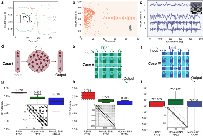
### Visual Description
## Chart/Diagram Type: Neuromorphic Computing Performance Analysis
### Overview
The image presents a series of plots and diagrams evaluating the performance of different neuromorphic computing architectures (RSNN FP32, Mosaic SNN FP32, and RRAM) on a spiking neural network task. It includes time-series data of input signals, schematic representations of network architectures, and box plots comparing test accuracy and inference speed.
### Components/Axes
* **a:** Time-series plot of two input channels (CH1 and CH2) over time (0-600 ms). The y-axis represents Input Channel ID (1 UP, 1 DN, 2 UP, 2 DN).
* **b:** Scatter plot of Input Channel ID (0-120) versus Time (0-100 ms). A microphone icon is present.
* **c:** Time-series plot of Input Channel ID (1-17) versus Environment Step (0-500).
* **d:** Schematic diagram illustrating Case i: a fully connected network with Input and Output layers.
* **e:** Schematic diagram illustrating Case ii: a network with a FP32 layer between Input and Output.
* **f:** Schematic diagram illustrating Case iii: a network with a FP32 layer and a processing unit between Input and Output.
* **g:** Box plot comparing Test Accuracy (0.75-1.00) for RSNN FP32, Mosaic SNN FP32, and RRAM. The x-axis represents the architecture.
* **h:** Box plot comparing Test Accuracy (0.55-0.80) for RSNN FP32, Mosaic SNN FP32, and RRAM. The x-axis represents the architecture. Inset plot shows a zoomed-in view of the data.
* **i:** Box plot comparing inference speed (640-780) for RSNN FP32, Mosaic SNN FP32, and RRAM. The x-axis represents the architecture. Inset plot shows a zoomed-in view of the data.
### Detailed Analysis or Content Details
**a:** The plot shows two fluctuating signals (CH1 and CH2). CH1 appears to have a higher frequency and amplitude than CH2. The signals are approximately periodic, with peaks and troughs occurring roughly every 100-200 ms.
**b:** The scatter plot shows a dense cluster of points, indicating a high frequency of activity in the lower Input Channel IDs (around 20-40) during the initial time period (0-20 ms). The density of points decreases over time, and the distribution becomes more spread out.
**c:** The plot shows fluctuating signals across multiple Input Channels. The signals appear noisy and irregular.
**d:** Case i depicts a network with a circular Input layer connected to an elliptical Output layer. The connections appear to be fully connected.
**e:** Case ii shows a network with an Input layer connected to a square FP32 layer, which is then connected to an Output layer.
**f:** Case iii shows a network with an Input layer connected to a square FP32 layer, which is then connected to a processing unit (represented by a square with a symbol), and finally to an Output layer.
**g:** RSNN FP32 has the highest median Test Accuracy at approximately 0.970, with a range from approximately 0.95 to 0.99. Mosaic SNN FP32 has a median Test Accuracy of approximately 0.936, with a range from approximately 0.91 to 0.96. RRAM has a median Test Accuracy of approximately 0.918, with a range from approximately 0.89 to 0.94.
**h:** RSNN FP32 has a median Test Accuracy of approximately 0.765, with a range from approximately 0.73 to 0.79. Mosaic SNN FP32 has a median Test Accuracy of approximately 0.729, with a range from approximately 0.69 to 0.76. RRAM has a median Test Accuracy of approximately 0.703, with a range from approximately 0.67 to 0.73.
**i:** RSNN FP32 has a median inference speed of approximately 736.972, with a range from approximately 725 to 750. Mosaic SNN FP32 has a median inference speed of approximately 723.86, with a range from approximately 700 to 740. RRAM has a median inference speed of approximately 725.835, with a range from approximately 680 to 760.
### Key Observations
* RSNN FP32 consistently outperforms Mosaic SNN FP32 and RRAM in terms of Test Accuracy in both box plots (g and h).
* RSNN FP32 also exhibits the highest inference speed, although the differences between the architectures are relatively small.
* The input signals (a, b, c) exhibit varying degrees of complexity and noise.
* The network architectures (d, e, f) demonstrate a progression from a simple fully connected network to more complex architectures incorporating FP32 layers and processing units.
### Interpretation
The data suggests that RSNN FP32 is the most effective architecture for the given spiking neural network task, achieving the highest Test Accuracy and inference speed. The inclusion of FP32 layers (as seen in Cases ii and iii) appears to improve performance compared to the fully connected network (Case i). The varying input signals (a, b, c) likely represent different types of sensory data or environmental conditions, and the network's ability to process these signals effectively is crucial for its overall performance. The box plots (g, h, i) provide a clear visualization of the performance differences between the architectures, highlighting the advantages of RSNN FP32. The inset plots in h and i provide a more detailed view of the data, revealing the distribution of values and potential outliers. The microphone icon in plot b suggests that the input data may be related to audio signals. The overall study aims to evaluate the trade-offs between accuracy and efficiency in different neuromorphic computing architectures.
</details>
even if we compare with digital approaches in more advanced technology nodes. This efficiency can be attributed to the Mosaic's in-memory routing approach resulting in low-energy routing memory access which is distributed in space. This reduces (i) the size of each router, and thus energy, compared to larger centralized routers employed in some platforms, and (ii) it avoids the use of CAMs, which consumes the majority of routing energy in some other spike-based routing mechanisms (Supplementary Note 2 ).
Neuromorphic platforms have each been designed to optimize different objectives [ 328 ], and the reason behind the energy efficiency of Mosaic in communication lies behind its explicit optimization for this very metric, thanks to its small-world connectivity layout. Despite this, as was shown in Fig. 5 . 4 , the Mosaic does not suffer from a considerable drop in accuracy, at least for problem sizes of the sensory processing applications on the edge. This implies that for these problems, large connectivity between the cores is not required, which can be exploited for reducing the energy.
The Mosaic's latency figure per router is comparable to the average latency of other platforms. Often, and in particular, for neural networks with sparse firing activity, this is a negligible factor. In applications requiring sensory processing of real-world slow-changing signals, the time constants dictating how quickly the model state evolves will be determined by the size of the Vlk in Fig. 5 . 2 , typically on the order of tens or hundreds of milliseconds. Although, the routing latency grows linearly with the number of hops in the networks, as shown in the final connectivity matrices of Fig. 5 . 4 g,h,i, the number of non-local connections decays down exponentially. Therefore, the latency of routing is always much less than the the time scale of the real-world signals on the edge, which is our target application.
The two final rows of Table 5 . 1 indicates the power consumption of the neuromorphic platforms in tasks A and B respectively. All the platforms are assumed to use a core (i.e., neuron tile) size of 32 neurons, and to have an N-hop energy cost equal to N times the 1 -hop value. The potential of the Mosaic is clearly demonstrated, whereby a power consumption of only a few hundreds of pico Watts is required, relative to a few nano/microwatts in the other neuromorphic platforms.
## 5 . 5 discussion
We have identified small-world graphs as a favorable topology for efficient routing, have proposed a hardware architecture that efficiently implements it, designed and fabricated memristor-based building blocks for the architecture in 130 nm technology, and report measurements and comparison to other approaches. We empirically quantified the impact of both the small-world neural network topology and low memristor precision on three diverse and challenging tasks representative of edge-AI settings. We also introduced an adapted machine learning strategy that enforces small-worldness and accounted for the low-precision of noisy RRAM devices. The results achieved across these tasks were comparable to those achieved by floating point precision models with unconstrained network connectivity.
Although the connectivity of the Mosaic is sparse, it still requires more number of routing nodes than computing nodes. However, the Routing Tiles are more compact than the neuron tiles, as they only perform binary classification. This means that the read-out circuitry does not require a large Signal to Noise Ratio (SNR), compared to the neuron tiles. This loosened requirement reduces the overhead of the Routing Tiles readout in terms of both area and power (Supplementary Note 9 ).
In this work, we have treated Mosaic as a standard RSNN, and trained it with BPTT using the surrogate gradient approximation, and simply added the loss terms that punish the network's dense connectivity to shape sparse graphs. Therefore, the potential computational advantages of small-world architectures do not necessarily emerge, and the performance of the network is mainly related to its number of parameters. In fact, we found that Mosaic requires more neurons, but about the same number of parameters, for the same accuracy as that of an RSNN on the same task. This confirms that taking advantage of small-world connectivity requires a novel training procedure, which we hope to develop in the future. Moreover, in this paper, we have benchmarked the Mosaic on sensory processing tasks and have proposed to take advantage of the small-worldness for energy savings thanks to the locality of information processing. However, from a computational perspective, these tasks do not necessarily take advantage of the smallwordness. In future works, one can foresee tasks that can exploit the small-world connectivity from a computational standpoint.
Mosaic favors local processing of input data, in contrast with conventional deep learning algorithms such as Convolutional and Recurrent Neural Networks. However, novel approaches in
◦ Assuming an average resistance value of 10 k Ω , and a read pulse 10 ns width. ∗ The same as energy per Synaptic Operation (SOP), numbers are taken from Basu, et al, 2022 [ 332 ]
| Mosaic | 130 nm ( 1 . 2 V) | on-chip | 400 fJ ◦ | 400 fJ | 1 . 6 pJ ◦ | 1 . 6 pJ ◦ | 25 ns | 25 ns | Yes | 809 pW ◦ 5 . 06 nW ◦ |
|-------------------|---------------------|-------------|------------|-----------------|-------------------|----------------------|---------------------|-------------------------------|--------------------------|--------------------------|
| Loihi [ 89 ] | 14 nm ( 0 . 75 V) | on-chip | 23 . 6 pJ | 60 . 416 pJ | 3 . 5 pJ | 10 . 24 pJ | 6 . 5 ns 60 . 35 ns | No | 7 . 71 nW | 248 . 41 nW |
| Dynap-SE [ 103 ] | 180 nm ( 1 . 8 V) | on-chip | 30 pJ | 13 . 4 pJ | 17 pJ (@ 1 . 3 V) | 17 pJ | 40 ns 28 . 88 ns | Yes | 10 . 02 nW | 322 . 7 nW |
| Neurogrid [ 331 ] | 180 nm ( 3 V) | on/off-chip | 1 nJ | 160 pJ | 14 nJ | 8 . 35 nJ | 20 ns 14 . 4 ns | No | 563 . 31 nW | 18 . 14 µ W |
| SpiNNaker [ 330 ] | 130 nm ( 1 . 2 V) | on-chip | 30 . 3 nJ | 30 . 3 nJ | 1 . 11 nJ | 1 . 11 nJ | 200 ps 200 ps | No | 9 . 85 µ W | 317 . 08 µ W |
| TrueNorth [ 329 ] | 28 nm ( 0 . 775 V) | on-chip | 26 pJ | 62 . 4 pJ | 2 . 3 pJ | 5 . 52 pJ . ns | 6 25 29 ns | No | 8 . 47 nW | 272 . 82 nW |
| Neuromorphic Chip | Technology | Routing | ∗ original | sct ∗∗ . 130 nm | ⋄ original | sct. 130 nm original | sct. 130 nm | Optimized for Small-Worldness | Routing Power for task A | Routing Power for task B |
| Neuromorphic Chip | Technology | Routing | 0 -hop | energy | 1 -hop | energy | 1 -hop latency | Optimized for Small-Worldness | Routing Power for task A | Routing Power for task B |
sct. = Scaled to
∗∗
⋄ = Numbers are taken from Moradi, et al, 2018 [ 103 ]
T able 5 . 1 : Comparison of spike-routing performance across neuromorphic platforms
deep learning, e.g., Vision Transformers with Local Attention [ 333 ] and MLP-mixers [ 334 ], treat input data in a similar way as the Mosaic, subdividing the input dimensions, and processing the resulting patches locally. This is also similar to how most biological system processes information in a local fashion, such as the visual system of fruit flies [ 335 ].
In the broader context, graph-based computing is currently receiving attention as a promising means of leveraging the capabilities of SNNs [ 336 -338 ]. The Mosaic is thus a timely dedicated hardware architecture optimized for a specific type of graph that is abundant in nature and in the real-world and that promises to find application at the extreme-edge.
## 5 . 6 methods
## Design, fabrication of Mosaic circuits
## 5 . 6 . 0 . 1 Neuron and routing column circuits
Both neuron and routing column share the common front-end circuit which reads the conductances of the RRAM devices. The RRAM bottom electrode has a constant DC voltage Vbot applied to it and the common top electrode is pinned to the voltage Vx by a rail-to-rail operational amplifier (OPAMP) circuit. The OPAMP output is connected in negative feedback to its non-inverting input (due to the 180 degrees phase-shift between the gate and drain of transistor M 1 in Fig. 5 . 2 ) and has the constant DC bias voltage Vtop applied to its inverting input. As a result, the output of the OPAMP will modulate the gate voltage of transistor M 1 such that the current it sources onto the node Vx will maintain its voltage as close as possible to the DC bias Vtop . Whenever an input pulse Vin < n > arrives, a current i in equal to ( Vx -Vbot ) Gn will flow out of the bottom electrode. The negative feedback of the OPAMP will then act to ensure that Vx = Vtop , by sourcing an equal current from transistor M 1 . By connecting the OPAMP output to the gate of transistor M 2, a current equal to i in , will therefore also be buffered, as i buf f , into the branch composed of transistors M 2 and M 3 in series. In the Routing Tile, this current is compared against a reference current, and if higher, a pulse is generated and transferred onwards. The current comparator circuit is composed of two current mirrors and an inverter (Fig. 5 . 3 b). In the neuron column, this current is injected into a CMOS differential-pair integrator synapse circuit model [ 188 ] which generates an exponentially decaying waveform from the onset of the pulse with an amplitude proportional to the injected current. Finally, this exponential current is injected onto the membrane capacitor of a CMOS leaky-integrate and fire neuron circuit model [ 339 ] where it integrates as a voltage (see Fig. 5 . 2 b). Upon exceeding a voltage threshold (the switching voltage of an inverter) a pulse is emitted at the output of the circuit. This pulse in turn feeds back and shunts the capacitor to ground such that it is discharged. Further circuits were required in order to program the device conductance states. Notably, multiplexers were integrated on each end of the column in order to be able to apply voltages to the top and bottom electrodes of the RRAM devices.
A critical parameter in both Neuron and Routing Tiles is the spike's pulse width. Minimizing the width of spikes assures maximal energy efficiency, but that comes at a cost. If the duration of the voltage pulse is too low, the readout current from the 1 T 1 R will be imprecise, and parasitic effects due to the metal lines in the array might even impede the correct propagation of either the voltage pulse or the readout current. For this reason, we thoroughly investigated the minimal pulse-width that allows spikes and readout currents to be reliably propagated, at a probability of 99 . 7 % ( 3 σ ). Extensive Monte Carlo simulation resulted in a spike pulse width of around 100 ns. Based on these SPICE simulations, we also estimated the energy consumption of Mosaic for the different tasks presented in Figure 5 . 4 .
## Fabrication/integration
The circuits described in the Results section have been taped-out in 130 nmtechnology at CEA-Leti, in a 200 mm production line. The Front End of the Line, below metal layer 4 , has been realized by ST-Microelectronics, while from the fifth metal layer upwards, including the deposition of the composites for RRAM devices, the process has been completed by CEA-Leti. RRAM devices are
composed of a 5 nm thick HfO 2 layer sandwiched by two 5 nm thick TiN electrodes, forming a TiN / HfO 2 / Ti / TiN stack. Each device is accessed by a transistor giving rise to the 1 T 1 R unit cell. The size of the access transistor is 650 nm wide. 1 T 1 R cells are integrated with CMOS-based circuits by stacking the RRAM cells on the higher metal layers. In the cases of the neuron and Routing Tiles, 1 T 1 R cells are organized in a small - either 2 x 2 or 2 x 4 - matrix in which the bottom electrodes are shared between devices in the same column and the gates shared with devices in the same row. Multiplexers operated by simple logic circuits enable to select either a single device or a row of devices for programming or reading operations. The circuits integrated into the wafer, were accessed by a probe card which connected to the pads of the dimension of [ 50 x 90 ] µ m 2 .
## RRAM characteristics
Resistive switching in the devices used in our paper are based on the formation and rupture of a filament as a result of the presence of an electric field that is applied across the device. The change in the geometry of the filament results in different resistive state in the device. A SET/RESET operation is performed by applying a positive/negative pulse across the device which forms/disrupts a conductive filament in the memory cell, thus decreasing/increasing its resistance. When the filament is formed, the cell is in the HCS, otherwise the cell is is the LCS. For a SET operation, the bottom of the 1 T 1 R structure is conventionally left at ground level, and a positive voltage is applied to the 1 T 1 R top electrode. The reverse is applied in the RESET operation. Typical values for the SET operation are Vgate in [ 0.9 -1.3 ] V , while the Vtop peak voltage is normally at 2.0 V . For the RESET operation, the gate voltage is instead in the [ 2.75, 3.25 ] V range, while the bottom electrode is reaching a peak at 3.0 V . The reading operation is performed by limiting the Vtop voltage to 0.3 V , a value that avoids read disturbances, while opening the gate voltage at 4.5 V .
## Mosaic circuit measurement setups
The tests involved analyzing and recording the dynamical behavior of analog CMOS circuits as well as programming and reading RRAM devices. Both phases required dedicated instrumentation, all simultaneously connected to the probe card. For programming and reading the RRAM devices, Source Measure Units (SMU)s from a Keithley 4200 SCS machine were used. To maximize stability and precision of the programming operation, SET and RESET are performed in a quasi-static manner. This means that a slow rising and falling voltage input is applied to either the Top (SET) or Bottom (RESET) electrode, while the gate is kept at a fixed value. To the Vtop ( t ) , Vbot ( t ) voltages, we applied a triangular pulse with rising and falling times of 1 sec and picked a value for Vgate . For a SET operation, the bottom of the 1 T 1 R structure is conventionally left at ground level, while in the RESET case the Vtop is equal to 0 V and a positive voltage is applied to Vbot . Typical values for the SET operation are Vgate in [ 0.9 -1.3 ] V , while the Vtop peak voltage is normally at 2.0 V . Such values allow to modulate the RRAM resistance in an interval of [ 5 -30 ] k Ω corresponding to the HCS of the device. For the RESET operation, the gate voltage is instead in the [ 2.75, 3.25 ] V range, while the bottom electrode is reaching a peak at 3.0 V .
The LCS is less controllable than the HCS due to the inherent stochasticity related to the rupture of the conductive filament, thus the HRS level is spread out in a wider [ 80 -1000 ] k Ω interval. The reading operation is performed by limiting the Vtop voltage to 0.3 V , a value that avoids read disturbances, while opening the gate voltage at 4.5 V .
Inputs and outputs are analog dynamical signals. In the case of the input, we have alternated two HP 8110 pulse generators with a Tektronix AFG 3011 waveform generator. As a general rule, input pulses had a pulse width of 1 µ s and rise/fall time of 50 ns . This type of pulse is assumed as the stereotypical spiking event of a Spiking Neural Network. Concerning the outputs, a 1 GHz Teledyne LeCroy oscilloscope was utilized to record the output signals.
## Mosaic layout-aware training via regularizing the loss function
We introduce a new regularization function, LM , that emphasizes the realization cost of short and long-range connections in the Mosaic layout. Assuming the Neuron Tiles are placed in a square layout, LM calculates a matrix H ∈ R j × i , expressing the minimum number of Routing Tiles used to connect a source neuron Nj to target neuron Ni , based on their Neuron Tile positions on Mosaic. Following this, a static mask S ∈ R j × i is created to exponentially penalize the long-range connections such that S = e β H -1, where β is a positive number that controls the degree of penalization for connection distance. Finally, we calculate the LM = ∑ S ⊙ W 2 , for the recurrent weight matrix W ∈ R j × i . Note that the weights corresponding to intra-Neuron Tile connections (where H = 0) are not penalized, allowing the neurons within a Neuron Tile to be densely connected. During the training, task-related cross-entropy loss term (total reward in case of RL) increases the network performance, while LM term reduces the strength of the neural network weights creating long-range connections in Mosaic layout. Starting from the 10 th epoch, we deterministically prune connections (replacing the value of corresponding weight matrix elements to 0 ) when their L 1 -norm is smaller than a fixed threshold value of 0 . 005 . This pruning procedure privileges local connections (i.e., those within a Neuron Tile or to a nearby Neuron Tile) and naturally gives rise to a small-world neural network topology. Our experiments found that gradient norm clipping during the training and reducing the learning rate by a factor of ten after 135 th epoch in classification tasks help stabilize the optimization against the detrimental effects of pruning.
## RRAM-aware noise-resilient training
The strategy of choice for endowing Mosaic with the ability to solve real-world tasks is offline training. This procedure consists of producing an abstraction of the Mosaic architecture on a server computer, formalized as a Spiking Neural Network that is trained to solve a particular task. When the parameters of Mosaic are optimized, in a digital floating-point32 -bits (FP 32 ) representation, they are to be transferred to the physical Mosaic chip. However, the parameters in Mosaic are constituted by RRAM devices, which are not as precise as the FP 32 counterparts. Furthermore, RRAMs suffer from other types of non-idealities such as programming stochasticity, temporal conductance relaxation, and read noise [ 312 , 315 -317 ].
To mitigate these detrimental effects at the weight transfer stage, we adapted the noise-resilient training method for RRAM devices [ 18 , 340 ]. Similar to quantization-aware training, at every forward pass, the original network weights are altered via additive noise (quantized) using a straight-through estimator. We used a Gaussian noise with zero mean and standard deviation equal to 5 % of the maximum conductance to emulate transfer non-idealities. The profile of this additive noise is based on our RRAM characterization of an array of 4096 RRAM devices [ 312 ], which are programmed with a program-and-verify scheme (up to 10 iterations) to various conductance levels then measured after 60 seconds for modeling the resulting distribution.
## ECG task description
The Mosaic hardware-aware training procedure is tested on a electrocardiogram arrhythmia detection task. The ECG dataset was downloaded from the MIT-BIH arrhythmia repository [ 318 ]. The database is composed of continuous 30 -minute recordings measured from multiple subjects. The QRS complex of each heartbeat has been annotated as either healthy or exhibiting one of many possible heart arrhythmias by a team of cardiologists. We selected one patient exhibiting approximately half healthy and half arrhythmic heartbeats. Each heartbeat was isolated from the others in a 700 ms time-series centered on the labelled QRS complex. Each of the two 700 ms channel signals were then converted to spikes using a delta modulation scheme [ 341 ]. This consists of recording the initial value of the time-series and, going forward in time, recording the time-stamp when this signal changes by a pre-determined positive or negative amount. The value of the signal at this time-stamp is then recorded and used in the next comparison forward
in time. This process is then repeated. For each of the two channels this results in four respective event streams - denoting upwards and downwards changes in the signals. During the simulation of the neural network, these four event streams corresponded to the four input neurons to the spiking recurrent neural network implemented by the Mosaic.
Data points were presented to the model in mini-batches of 16 . Two populations of neurons in two Neuron Tiles were used to denote whether the presented ECG signals corresponded to a healthy or an arrhythmic heartbeat. The softmax of the total number of spikes generated by the neurons in each population was used to obtain a classification probability. The negative log-likelihood was then minimized using the categorical cross-entropy with the labels of the signals.
## Keyword Spotting task description
For keyword spotting task, we used SHD dataset ( 20 classes, 8156 training, 2264 test samples). Each input example drawn from the dataset is sampled three times along the channel dimension without overlap to obtain three augmentations of the same data with 256 channels each. The advantage of this method is that it allows feeding the input stream to fewer Neuron Tiles by reducing the input dimension and also triples the sizes of both training and testing datasets.
We set the simulation time step to 1 ms in our simulations. The recurrent neural network architecture consists of 2048 LIF neurons with 45 ms membrane time constant. The neurons are distributed into 8 x 8 Neuron Tiles with 32 neurons each. The input spikes are fed only into the neurons of the Mosaic layout's first row ( 8 tiles). The network prediction is determined after presenting each speech data for 100 ms by counting the total number of spikes from 20 neurons (total number of classes) in 2 output Neuron Tiles located in the bottom-right of the Mosaic layout. The neurons inside input and output Neuron Tiles are not recurrently connected. The network is trained using BPTT on the loss L = LCE + λ LM , where LCE is the cross-entropy loss between input logits and target and LM is the Mosaic-layout aware regularization term. We use batch size of 512 and suitably tuned hyperparameters.
## Reinforcement Learning task description
In the RL experiments, we test the versatility of a Mosaic-optimized RSNN on a continuous action space motor-control task, half-cheetah, implemented using the BRAX physics engine for rigid body simulations [ 342 ]. At every timestep t , environment provides an input observation vector o t ∈ R 25 and a scalar reward value r t . The goal of the agent is to maximize the expected sum of total rewards R = ∑ 1000 t = 0 r t over an episode of 1000 environment interactions by selecting action a t ∈ R 7 calculated by the output of the policy network. The policy network of our agent consists of 256 recurrently connected LIF neurons, with a membrane decay time constant of 30 ms. The neuron placement is equally distributed into 16 Neuron Tiles to form a 7 x 7 Mosaic layout. We note that for simulation purposes, selecting a small network of 16 Neuron Tiles with 16 neurons each, while not optimal in terms of memory footprint (Eq. 5 . 2 ), was preferred to fit the large ES population within the constraints of single GPU memory capacities. At each time step, the observation vector o t is accumulated into the membrane voltages of the first 25 neurons of two upper left input tiles. Furthermore, action vector a t is calculated by reading the membrane voltages of the last seven neurons in the bottom right corner after passing tanh non-linearity.
We considered Evolutionary Strategies (ES) as an optimization method to adjust the RSNN weights such that after the training, the agent can successfully solve the environment with a policy network with only locally dense and globally sparse connectivity. We found ES particularly promising approach for hardware-aware training as (i) it is blind to non-differentiable hardware constraints e.g., spiking function, quantizated weights, connectivity patterns, and (ii) highly parallelizable since ES does not require spiking variable to be stored for thousand time steps compared to BPTT that explicitly calculates the gradient. In ES, the fitness function of an offspring is defined as the combination of total reward over an episode, R and realization cost of short and long-range connections LM (same as KWS task), such that F = R -λ LM . We used the population
size of 4096 (with antithetic sampling to reduce variance) and mutation noise standard deviation of 0 . 05 . At the end of each generation, the network weights with L 0-norm smaller than a fixed threshold are deterministically pruned. The agent is trained for 1000 generations.
## Calculation of memory footprint
We calculate the Mosaic architecture's Memory Footprint (MF) in comparison to a large crossbar array, in building small-world graphical models.
To evaluate the MF for one large crossbar array, the total number of devices required to implement any possible connections between neurons can be counted - allowing for any RSNN to be mapped onto the system. Setting N to be the number of neurons in the system, the total possible number of connections in the graph is MFref = N 2 .
For the Mosaic architecture, the number of RRAM cells (i.e., the MF) is equal to the number of devices in all the Neuron Tiles and Routing Tiles: MFmosaic = MFNeuronTiles + MFRoutingTiles .
Considering each Neuron Tile with k neurons, each Neuron Tile contributes to 5 k 2 devices (where the factor of 5 accounts for the four possible directions each tile can connect to, plus the recurrent connections within the tile). Evenly dividing the N total number of neurons in each Neuron Tile gives rise to T = ceil ( N / k ) required Neuron Tiles. This brings the total number of devices attributed to the Neuron Tile to T · 5 k 2 .
The problem can then be re-written as a function of the geometry. Considering Fig. 5 . 1 g, let i be an integer and ( 2 i + 1 ) 2 the total number of tiles. The number of Neuron Tiles can be written as T = ( i + 1 ) 2 , as we consider the case where Neuron Tiles form the outer ring of tiles. As a consequence, the number of Routing Tiles is R = ( 2 i + 1 ) 2 -( i + 1 ) 2 . Substituting such values in the previous evaluations of MFNeuronTiles + MFRoutingTiles and remembering that k < N · T , we can impose that MFMosaic = MFNeuronTiles + MFRoutingTiles < MFMFref .
The number of Routing Tiles that connects all the Neuron Tiles depends on the geometry of the Mosaic systolic array. Here, we assume Neuron Tiles assembled in a square, each with a Routing Tile on each side. We consider R to be the number of Routing Tiles with ( 4 k ) 2 devices in each. This brings the total number of devices related to Routing Tiles up to MFRoutingTiles = R · ( 4 k ) 2 .
This results in the following expression:
$$M F _ { M o s a i c } = M F _ { N e u r o n T i l e s } + M F _ { R o u t i n g T i l e s } < M F _ { r e f e r e n c e }$$
$$\begin{array} { l } ( i + 1 ) ^ { 2 } \, ( 5 k ^ { 2 } ) + [ ( 2 i + 1 ) ^ { 2 } - ( i + 1 ) ^ { 2 } ] \, ( 4 k ) ^ { 2 } < ( k \, ( i + 1 ) ^ { 2 } ) ^ { 2 } \end{array} \quad ( 5 . 2 )$$
This expression can then be evaluated for i , given a network size, giving rise to the relationships as plotted in Fig. 5 . 1 g in the main text.
<details>
<summary>Image 36 Details</summary>

### Visual Description
Icon/Small Image (54x82)
</details>
In this thesis, I explored implementing neural computation on mixed-signal hardware with in-memory computing capabilities. Neural computation (i.e., inference, learning and routing) is fundamentally memory-centric, and von Neumann architecture's separation of memory and computation is a major contributor to modern neural networks' overall energy consumption and latency. Based on this observation, we investigated offloading critical neural computations directly onto the raw analog dynamics of resistive memory technologies.
This thesis begins by addressing the challenge of online training of feedforward spiking neural networks implemented using intrinsically 1 -bit RRAM devices. In Chapter 2 , we presented a novel memristor programming technique to precisely control the filament formation in RRAMs devices, increasing their effective bit resolution for more stable training dynamics and improved performance. The versatility of this technique was further demonstrated by applying it to novel perovskite memristors in Chapter 4 , achieving an even more linear device response.
In Chapter 3 , we tackled the temporal credit assignment problem in RSNNs on an analog substrate. We developed a simulation framework based on a comprehensive statistical model of the PCM crossbar array, capturing major non-linearities of memristors. This framework enabled the simulation of device responses to various weight programming techniques designed to mitigate these non-idealities. Using this framework, we trained a RSNN with the e-prop local learning rule, demonstrating that gradient accumulation is crucial for accurately reflecting weight updates on memristive devices - a finding later validated on a real neuromorphic chip. While our solution, which relies on a digital coprocessor, incurs an energy cost, it motivates the development of future devices with intrinsic accumulation capabilities, potentially through conductance or charge storage. Additionally, we introduced PCM-trace, a scalable implementation of synaptic eligibility traces for local learning using the volatile regime of PCM devices.
In Chapter 4 , we presented a discovery of a novel memristor capable of switching between volatile and non-volatile modes. This reconfigurable memristor, based on halide perovskite nanocrystals, offers a significant advancement in emerging memory technologies, enabling the implementation of both static and dynamic neural parameters with the same material and fabrication technique.
Finally, in Chapter 5 , we introduced Mosaic, a memristive systolic architecture for in-memory computing and routing. Mosaic efficiently implements small-world graph connectivity, demonstrating superior energy efficiency in spike routing compared to other hardware platforms. Additionally, we introduced a hardware-layout aware training method that takes the physical layout of the chip into account while optimizing the neural network weights.
## Discussion and Outlook
I conclude by highlighting significant limitations of neural computation on analog substrates, which serve as a foundation for future research.
- 1 . Discovering efficient material and peripheral circuits Although our experiments demonstrate the potential of learning on analog substrates using mature RRAM and PCM technologies, significant challenges remain in achieving efficiency of digital accelerators. Limited bit resolution inherent to these devices necessitates energy-intensive gradient accumulation on a co-processor, hindering overall efficiency. As the analog device sizes shrink, this problem is expected to become more pronounced. While improving bit precision can enhance accuracy, it alone won't guarantee efficient analog learning. Additionally, the high WRITE operation energy of memristors needs to be lowered to match the low programming energies of SRAM. Finally, it's worth noting that scaling trends are primarily driven by peripheral circuitry, rather than the memory cells, necessitating area optimization on the periphery to achieve cost-effective fabrication. Future research should prioritize addressing these challenges, relatively in this order to achieve learning performances competitive with digital accelerators.
- 2 . Local learning in unconventional networks The co-design approach is driving neural architectures to be increasingly tailored to hardware for efficiency. For example quantization is adapted to reduce memory footprint, State Space Models (SSMs) leverage recurrency and improve arithmetic intensity (FLOPs/byte) in digital and spiking neurons convert analog membrane voltage to binary spikes and eliminate the need for ADC in analog. It seems reasonable to expect more such primitives to emerge potentially leveraging sparsity or stochasticity. This raises the question of how to design local learning rules for unconventional future architectures. Can a single learning rule provide an end-to-end solution, or can credit assignment be modularized for subgraphs? Recent work suggests that exploring such directions may yield valuable insights and unexpected performance tradeoffs [ 69 , 71 , 72 , 343 , 344 ].
- 3 . Mismatch between silicon and brain Biological plausibility and silicon efficiency represent distinct optimization goals. While silicon dynamics outpace neuronal dynamics in raw speed 1 , it falls short in matching the brain's power efficiency and parallelism. I argue that while mimicking the brain's intricacies may be scientifically interesting, it is not necessarily an ideal blueprint for either silicon efficiency or intelligence. Instead, focusing on silicon efficiency allows us to leverage the unique strengths of this substrate. This will naturally lead to design principles that are common, such as minimizing wiring and localizing computation, however, we are not bound by the specific artifacts of biological evolution. So it remains an open question which criteria from neuroscience should inform hardware design improvements.
- 4 . Remembering the Jevons Paradox While hardware-algorithm co-design aims to enhance the power efficiency of on-device intelligence, the Jevons Paradox suggests that this may inadvertently increase overall AI energy consumption due to increased demand [ 345 ]. This is a phenomenon occurred in the past, where increasing efficiency of coal engines led to more coal consumption. This raises important questions for future investigation about potential societal and governmental regulations to mitigate the environmental impact, or more exotic technological deployment strategies that keep carbon footprint of AI on the Earth minimal.
1 Electron mobility in transistors is at least 10 7 time faster than ion transport rate in neuron channels.
At the time of writing, learning on mixed-signal hardware with memristive weights hasn't reached the efficiency of digital accelerators. It seems probable that in the future the scene will evolve as the material design and fabrication technology quickly mature. Nevertheless, it will remain an exciting playground where intelligence meets the raw, unfiltered physics of computation.
<details>
<summary>Image 37 Details</summary>

### Visual Description
\n
## Image: Letter "A"
### Overview
The image displays a single, stylized capital letter "A" in a dark gray color against a white background. There is no accompanying data, chart, or diagram. It is a simple visual representation of the letter.
### Components/Axes
There are no axes, legends, or scales present. The sole component is the letter "A" itself.
### Detailed Analysis or Content Details
The letter "A" is rendered in a serif typeface. The left stroke is thicker than the right stroke, and the crossbar is positioned approximately two-thirds of the way up the left stroke. The overall shape is slightly elongated vertically. The color is a consistent dark gray, appearing approximately as #404040.
### Key Observations
The image contains no quantifiable data or trends. It is a static visual element.
### Interpretation
The image serves as a basic representation of the letter "A". Without further context, it's difficult to determine its purpose. It could be a logo element, a typographic sample, or simply a visual placeholder. The stylistic choices (serif typeface, stroke weight variation) suggest a deliberate aesthetic choice, potentially aiming for a classic or elegant appearance. The lack of additional information limits a deeper interpretation. It is a symbol, but its meaning is entirely dependent on the context in which it is used.
</details>
We present here some additional results to complement the main results discussed in the previous sections.
appendix 1 : online training of spiking recurrent neural networks with phase -change memory synapses supplementary note 1 We implemented the PCM crossbar array simulation framework in PyTorch [ 107 ], which can be used for both the inference and the training of ANNs or SNNs. Built on top of the statistical model introduced by Nandakumar et al. [ 81 ], our crossbar model supports asynchronous SET, RESET and READ operations over entire crossbar structures and simultaneously keep tracks of the temporal evolution of device conductances.
A single crossbar array consists of P × Q nodes (each node representing a synapse), where single node has 2 N memristors arranged using the differential architecture ( N potentiation, N depression devices). Each memristor state is represented by four variables, t p for storing the last time the device is written (which is used to calculate the effect of the drift), count for counting how many times it has written (to be used later in the arbiter of N-memristor architectures), Pmem for its programming history (required by the PCM model) and G for representing the conductance of the the device at T 0 seconds later after the last programming time. The initial conductances of PCM devices in the crossbar array are assumed to be iterativelly programmed to HRS, sampled from a Normal distribution N ( µ = 0.1, σ = 0.01 ) µ S.
The PCM crossbar simulation framework supports three major functions: READ, SET and RESET. The READ function takes the pulse time of the applied READ pulse, t , and calculates the effect of drift based on the last programming time t p . Then, it adds the conductance-dependent READ noise and returns the conductance values of whole array. The SET function takes the timing information of the applied SET pulse, together with a mask of shape ( 2 × N × P × Q ) and calculates the effect of the application of a single SET pulse on the PCM devices that are selected with the mask. Finally, the RESET function initializes all the state variables of devices selected with a mask and initializes the conductances using a Normal distribution N ( µ = 0.1, σ = 0.01 ) µ S.
supplementary note 2 READ and WRITE operations to simulated PCM devices in the crossbar model are stochastic and subject to the temporal conductance drift. Additionally, PCM devices offer a very limited bit precision. Therefore, to ease the network training procedure, especially the hyperparameter tuning, we developed the perf-mode . When crossbar model is operated in perf-mode , all stochasticity sources and the conductance drift are disabled. READ operations directly access the device conductance without 1/ f noise and drift, whereas SET operations increase the device conductance as
$$G _ { N } = G _ { N - 1 } + \frac { G _ { M A X } } { 2 ^ { C B _ { R E S } } } , & & ( A . 1 )$$
where, GMAX is the maximum PCM conductance set to 12 µ S (conductivity boundaries are determined based on the device measurements from [ 81 ]), and CBRES is the desired bit-resolution of a single PCM device. In a nutshell, the perf-mode turns PCMs into an ideal memory cells corresponding to a digital memory with a limited bit precision.
supplementary note 3 Here, we demonstrate the impact of using multiple memristor devices per synapse (arranged in differential configuration) on the precision of targeted programming updates. Specifically, we modeled synapses with N = 1, 4, 8 PCM devices and programmed them from initial conditions of integer conductance values Gsource ∈ {-10, 10 } µ S to integer
<details>
<summary>Image 38 Details</summary>
### Visual Description
## Line Chart: Performance Comparison Over Time
### Overview
This image presents a line chart comparing the performance of two modes, "PCM Model" and "Perf Mode," over a period of 800 seconds. The y-axis represents a performance metric labeled "G (µs)", likely representing latency or execution time. The x-axis represents time in seconds.
### Components/Axes
* **X-axis:** Time (s), ranging from 0 to 800 seconds. Marked at intervals of 100 seconds.
* **Y-axis:** G (µs), ranging from 0 to 12 µs. Marked at intervals of 2 µs.
* **Legend:** Located in the top-left corner.
* "PCM Model" - represented by a blue line.
* "Perf Mode" - represented by an orange line.
* **Grid:** A light gray grid is present, aiding in reading values.
### Detailed Analysis
**PCM Model (Blue Line):**
The blue line representing "PCM Model" starts at approximately 0.2 µs at time 0 seconds. It initially fluctuates slightly, then exhibits a series of step-like increases.
* At approximately 100 seconds, the value increases to around 1.8 µs.
* Around 200 seconds, it rises to approximately 4.5 µs.
* At 300 seconds, it increases to around 5.8 µs.
* Around 400 seconds, it rises to approximately 6.2 µs.
* At 500 seconds, it increases to around 7.5 µs.
* Around 600 seconds, it rises to approximately 8.5 µs.
* At 700 seconds, it increases to approximately 9.5 µs.
* Finally, at 800 seconds, it ends at approximately 10.5 µs.
Throughout the entire duration, the line exhibits some degree of fluctuation around these step-like increases.
**Perf Mode (Orange Line):**
The orange line representing "Perf Mode" starts at approximately 0.1 µs at time 0 seconds. It also exhibits step-like increases, but generally at a higher level than the "PCM Model".
* At approximately 100 seconds, the value decreases to around 0.8 µs.
* Around 200 seconds, it rises to approximately 2.5 µs.
* At 300 seconds, it increases to around 7.5 µs.
* Around 400 seconds, it rises to approximately 7.8 µs.
* At 500 seconds, it increases to around 10.2 µs.
* Around 600 seconds, it rises to approximately 10.8 µs.
* At 700 seconds, it rises to approximately 11.5 µs.
* Finally, at 800 seconds, it ends at approximately 12 µs.
Similar to the "PCM Model", the "Perf Mode" line also shows fluctuations around these step-like increases.
### Key Observations
* "Perf Mode" consistently exhibits higher values of "G (µs)" than "PCM Model" for most of the duration, indicating potentially higher latency or execution time.
* Both modes show a general increasing trend in "G (µs)" over time, suggesting a performance degradation or increased load.
* The step-like increases in both lines suggest discrete changes in operating conditions or workload.
* The fluctuations around the step-like increases indicate variability in performance within each mode.
### Interpretation
The chart demonstrates a performance comparison between two modes, "PCM Model" and "Perf Mode," over time. The increasing trend in "G (µs)" for both modes suggests a potential performance bottleneck or increasing load on the system. The consistently higher values for "Perf Mode" could indicate that this mode is more resource-intensive or has inherent performance limitations. The step-like increases suggest that the system is transitioning between different states or handling different workloads. The fluctuations within each mode could be due to variations in input data, background processes, or other factors.
The data suggests that while "Perf Mode" might offer certain advantages, it comes at the cost of increased latency or execution time. Further investigation is needed to understand the root cause of the performance degradation and the reasons for the step-like increases. The chart provides valuable insights into the behavior of the two modes and can be used to optimize system performance.
</details>
- (a) Comparison of the full PCM model and its perf-mode equivalent after 8 consecutive SET pulses.
- (b) Comparison of the full PCM model and its perf-mode equivalent after 8 consecutive SET pulses, averaged over 300 measurements showing the effect of drift.
<details>
<summary>Image 39 Details</summary>
### Visual Description
## Line Chart: G (µs) vs. Time (s)
### Overview
This image presents a line chart comparing two data series, "PCM Model" and "Perf Mode", plotted against time. The y-axis represents 'G' measured in microseconds (µs), and the x-axis represents time in seconds (s). The chart displays the change in 'G' over time for both models.
### Components/Axes
* **X-axis:** Time (s), ranging from 0 to 300 seconds.
* **Y-axis:** G (µs), ranging from 0 to 13 µs.
* **Data Series 1:** "PCM Model" - Represented by a blue line with triangular markers.
* **Data Series 2:** "Perf Mode" - Represented by an orange line with square markers.
* **Legend:** Located in the bottom-right corner, identifying the two data series and their corresponding colors.
### Detailed Analysis
**PCM Model (Blue Line):**
The blue line starts at approximately 2.2 µs at time 0s. It initially increases rapidly, reaching around 7.5 µs by 80s. After 80s, the line exhibits a decreasing trend, leveling off to approximately 7 µs by 300s. The slope of the line decreases over time, indicating a slowing rate of change.
* (0s, 2.2 µs)
* (20s, 3.8 µs)
* (40s, 5.4 µs)
* (60s, 6.6 µs)
* (80s, 7.5 µs)
* (100s, 7.8 µs)
* (150s, 7.3 µs)
* (200s, 7.1 µs)
* (250s, 7.0 µs)
* (300s, 7.0 µs)
**Perf Mode (Orange Line):**
The orange line starts at approximately 0.2 µs at time 0s. It increases in a series of steps, reaching approximately 12.5 µs by 80s. From 80s to 300s, the line remains relatively constant at around 12.5 µs.
* (0s, 0.2 µs)
* (10s, 1.0 µs)
* (20s, 2.0 µs)
* (30s, 3.0 µs)
* (40s, 4.0 µs)
* (50s, 5.0 µs)
* (60s, 6.0 µs)
* (70s, 8.0 µs)
* (80s, 12.5 µs)
* (90s, 12.5 µs)
* (150s, 12.5 µs)
* (200s, 12.5 µs)
* (250s, 12.5 µs)
* (300s, 12.5 µs)
### Key Observations
* The "Perf Mode" consistently exhibits a higher 'G' value than the "PCM Model" throughout the entire duration of the chart.
* The "PCM Model" shows a decreasing rate of increase in 'G' over time, while "Perf Mode" plateaus after an initial rapid increase.
* The "Perf Mode" increases in discrete steps, suggesting a quantized or staged adjustment process.
### Interpretation
The chart likely represents the performance characteristics of two different systems or modes of operation. "PCM Model" could be a predictive or simulated model, while "Perf Mode" represents the actual performance of a system. The initial increase in both models suggests a warm-up or initialization phase. The plateau in "Perf Mode" indicates that the system has reached a stable operating point. The decreasing rate of increase in "PCM Model" might suggest that the model is converging towards a steady state or that the system is experiencing diminishing returns. The significant difference in 'G' values between the two suggests that "Perf Mode" is significantly more efficient or capable than the "PCM Model" in terms of the measured parameter 'G'. The stepped increases in "Perf Mode" could indicate discrete performance levels or adjustments made by the system.
</details>
F igure A. 1 : The PCM crossbar model supports both the full PCM model from [ 81 ] and its corresponding simplified version as an ideal digital memory in perf-mode .
<details>
<summary>Image 40 Details</summary>
### Visual Description
\n
## Heatmaps: Mean and Standard Deviation of Conductance
### Overview
The image presents two heatmaps side-by-side. The left heatmap displays the mean values, while the right heatmap displays the standard deviation (STD). Both heatmaps represent a two-dimensional relationship between "source conductance" and "target conductance", both measured in μG (micro-Siemens). The color intensity in each heatmap corresponds to the magnitude of the mean or standard deviation value.
### Components/Axes
Both heatmaps share the same structure:
* **X-axis:** "target conductance (μG)" ranging from -10 to 10, with increments of 1.
* **Y-axis:** "source conductance (μG)" ranging from -10 to 10, with increments of 1.
* **Color Scale (Left Heatmap):** Represents the "Mean, (Error=2.90)". The scale ranges from approximately -5.5 to 7.5. Colors transition from dark purple (low values) through red (intermediate values) to yellow (high values).
* **Color Scale (Right Heatmap):** Represents "STD". The scale ranges from approximately 0 to 35. Colors transition from light yellow (low values) through red (intermediate values) to dark purple (high values).
* **Data Points:** Each cell in the grid represents a specific combination of source and target conductance, with the cell's color indicating the corresponding mean or standard deviation value.
### Detailed Analysis or Content Details
**Left Heatmap (Mean):**
The heatmap shows a generally diagonal pattern. Values are more negative when both source and target conductance are negative, and more positive when both are positive.
* **Top-Left Corner (-10,-10):** Approximately -5.45
* **Center (0,0):** Approximately 0.05
* **Bottom-Right Corner (10,10):** Approximately 7.45
* **Along the diagonal (e.g., -5,-5):** Approximately -2.5
* **Along the diagonal (e.g., 5,5):** Approximately 2.5
* **Row 1 (Source Conductance = -10):** Values range from -5.45 to -1.35, increasing from left to right.
* **Row 10 (Source Conductance = 10):** Values range from 1.35 to 7.45, increasing from left to right.
* **Column 1 (Target Conductance = -10):** Values range from -5.45 to 1.35, increasing from top to bottom.
* **Column 10 (Target Conductance = 10):** Values range from -1.35 to 7.45, increasing from top to bottom.
**Right Heatmap (Standard Deviation):**
The heatmap shows a strong diagonal pattern, with higher standard deviations along the diagonal and lower standard deviations near the corners.
* **Top-Left Corner (-10,-10):** Approximately 32.5
* **Center (0,0):** Approximately 10.1
* **Bottom-Right Corner (10,10):** Approximately 35
* **Along the diagonal (e.g., -5,-5):** Approximately 22.5
* **Along the diagonal (e.g., 5,5):** Approximately 25
* **Row 1 (Source Conductance = -10):** Values range from 32.5 to 12.5, decreasing from left to right.
* **Row 10 (Source Conductance = 10):** Values range from 12.5 to 35, decreasing from left to right.
* **Column 1 (Target Conductance = -10):** Values range from 32.5 to 12.5, decreasing from top to bottom.
* **Column 10 (Target Conductance = 10):** Values range from 12.5 to 35, decreasing from top to bottom.
### Key Observations
* The mean values are generally symmetric around the origin (0,0).
* The standard deviation is highest when source and target conductances are similar in magnitude (along the diagonal).
* The standard deviation is lowest when either source or target conductance is close to zero.
* The error associated with the mean is 2.90, suggesting a consistent level of uncertainty across the data.
### Interpretation
The data suggests a linear relationship between source and target conductance, as evidenced by the diagonal pattern in the mean heatmap. The positive slope indicates that as both source and target conductance increase, the mean value also increases. The high standard deviation along the diagonal suggests that there is significant variability in the data when source and target conductances are similar. This could be due to noise in the measurements or inherent variability in the system being studied. The lower standard deviation near the corners indicates that the data is more consistent when either source or target conductance is close to zero.
The error value of 2.90 provides a measure of the uncertainty in the mean values. This information is important for assessing the reliability of the results and for making informed decisions based on the data. The combination of mean and standard deviation heatmaps provides a comprehensive picture of the relationship between source and target conductance, allowing for a more nuanced understanding of the underlying system. The data suggests that the relationship is strongest and most predictable when one of the conductances is near zero, and becomes more variable as both conductances increase.
</details>
F igure A. 2 : Multi-memristor configuration with 1 PCM(one depression and one potentiation) per synapse
conductance values Gtarget ∈ {-10, 10 } µ S using the multi-memristor update scheme described in Section 3 . 1 . 3 . 2 . The effective conductance of a synapse is calculated by Gsyn = ∑ N i = 0 G + i -∑ N i = 0 G -i , however we normalized the conductance across 1 -PCM, 4 -PCM and 8 -PCM architectures for an easier comparison, such that Gsyn = 1 N ( ∑ N i = 0 G + i -∑ N i = 0 G -i ) .
Our empirical results verifies the claim of Boybat et al. [ 109 ] that the standard deviation and the update resolution of the write process decreases by √ N .
supplementary note 4 In the differential architectures, consecutive SET pulses applied to positive and negative memristors may cause the saturation of the synaptic conductance and block further updates. The saturation effect is more apparent when a single synapse gets 10 + updates in one direction (potentiation or depression) during the training. For example, this effect is clearly visible in SupplFig. A. 2 , Fig. A. 3 and Fig. A. 4 , when the source conductance and target conductances differ by more than 8 -10 µ S.
We implemented a weight update scheme denoted as the update-ready criterion, which aims to prevent conductance saturation while applying single large updates. Before doing the update, we read both positive and negative pair conductances, and check if the target update is possible. If not, we reset both devices, calculate the new target and apply the number of pulses accordingly. For example, given G + = 8 µ S and G -= 4 µ S and the targeted update + 6 µ S, the algorithm decides to reset both devices because G + can't be increased up to 14 µ S. After both devices are
<details>
<summary>Image 41 Details</summary>
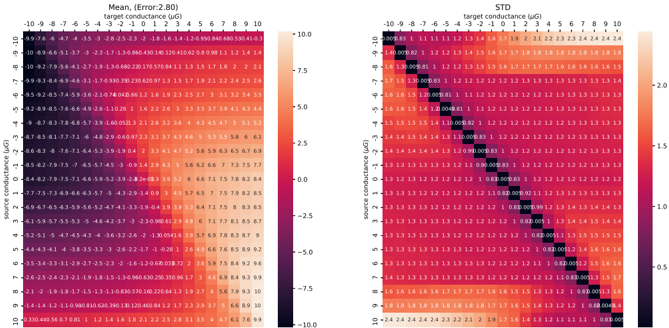
### Visual Description
\n
## Heatmaps: Mean and Standard Deviation of Conductance
### Overview
The image presents two heatmaps side-by-side. The left heatmap displays the mean values, while the right heatmap displays the standard deviation. Both heatmaps represent a two-dimensional relationship between "source conductance" and "target conductance", both measured in µG (micrograms). The color scale indicates the magnitude of the values, with darker colors representing lower values and lighter/redder colors representing higher values.
### Components/Axes
Both heatmaps share the same structure:
* **X-axis:** Target Conductance (µG), ranging from -10 to 10, with increments of 1.
* **Y-axis:** Source Conductance (µG), ranging from -10 to 10, with increments of 1.
* **Color Scale (Left):** Represents the Mean value. Ranges from approximately -10 to 10.
* **Color Scale (Right):** Represents the Standard Deviation. Ranges from approximately 0 to 20.
* **Title (Left):** "Mean, (Error:2.80)"
* **Title (Right):** "STD"
### Detailed Analysis or Content Details
**Left Heatmap (Mean)**
The heatmap shows a clear diagonal pattern. Values are generally negative when both source and target conductance are negative, and positive when both are positive. The values increase in magnitude as you move away from the origin (0,0) along the diagonal.
Here's a sampling of values (approximate, read from the heatmap):
* (-10, -10): -9.74
* (-10, 0): -2.2
* (-10, 10): 1.41
* (0, -10): -2.2
* (0, 0): 0.0
* (0, 10): 1.41
* (10, -10): 1.41
* (10, 0): 2.2
* (10, 10): 9.74
* (-5, -5): -4.7
* (5, 5): 4.7
* (-2, 2): 0.2
* (2, -2): -0.2
**Right Heatmap (Standard Deviation)**
The standard deviation heatmap shows a strong diagonal pattern with high values. The highest standard deviation values are concentrated along the diagonal where source and target conductance are similar. The standard deviation is generally lower when the source and target conductance have opposite signs.
Here's a sampling of values (approximate, read from the heatmap):
* (-10, -10): 19.5
* (-10, 0): 11.5
* (-10, 10): 5.5
* (0, -10): 11.5
* (0, 0): 1.5
* (0, 10): 5.5
* (10, -10): 5.5
* (10, 0): 11.5
* (10, 10): 19.5
* (-5, -5): 14.5
* (5, 5): 14.5
* (-2, 2): 3.5
* (2, -2): 3.5
### Key Observations
* **Mean:** The mean values exhibit a symmetrical pattern around the origin. The magnitude of the mean increases as the absolute values of both source and target conductance increase.
* **Standard Deviation:** The standard deviation is highest when source and target conductance are similar in magnitude and sign. This suggests that the relationship between source and target conductance is most consistent when they are both positive or both negative and have similar values. The standard deviation is lowest near the origin and when the source and target conductance have opposite signs.
* **Correlation:** The two heatmaps are related. The high standard deviation along the diagonal in the right heatmap corresponds to regions where the mean values are also relatively high in the left heatmap.
### Interpretation
The data suggests a strong correlation between source and target conductance. The mean heatmap indicates that the relationship is approximately linear, with a positive slope. The standard deviation heatmap reveals that the consistency of this relationship is highest when both conductances are similar in magnitude and sign.
The high standard deviation along the diagonal suggests that the system is most predictable when the source and target conductances are aligned. The lower standard deviation when the conductances have opposite signs indicates that the relationship becomes more variable and less predictable in those scenarios.
The "Error: 2.80" in the title of the mean heatmap likely refers to the estimated error associated with the mean values. This suggests that the values presented are based on some form of averaging or estimation, and there is an inherent uncertainty of approximately 2.80 units.
The data could represent a physical system where conductance is transferred or coupled between two components. The observed patterns could be due to factors such as resistance, capacitance, or other physical properties of the system. Further analysis and context would be needed to fully understand the underlying mechanisms.
</details>
F igure A. 3 : Multi-memristor configuration with 8 PCM (four depression and four potentiation) per synapse
<details>
<summary>Image 42 Details</summary>
### Visual Description
\n
## Heatmaps: Conductance Correlation Analysis
### Overview
The image presents two heatmaps side-by-side, visualizing the correlation between source and target conductance. The left heatmap displays the 'Mean' correlation with an associated error of 2.77, while the right heatmap shows the 'STD' (Standard Deviation) of the correlation. Both heatmaps use a color scale to represent the correlation strength, ranging from approximately -10.0 to 10.0 on both the x and y axes.
### Components/Axes
Both heatmaps share the same structure:
* **X-axis:** Target Conductance (µG), ranging from -10 to 10, with increments of 1.
* **Y-axis:** Source Conductance (µG), ranging from -10 to 10, with increments of 1.
* **Color Scale:** Represents the correlation value.
* Left Heatmap (Mean): Ranges from approximately -10.0 (dark blue) to 10.0 (dark red).
* Right Heatmap (STD): Ranges from approximately -2.21 (dark blue) to 1.75 (dark red).
* **Title:** Left: "Mean, (Error:2.77)". Right: "STD".
### Detailed Analysis or Content Details
**Left Heatmap (Mean):**
The heatmap shows a strong positive correlation along the diagonal, where source and target conductance are equal. Values along the diagonal are approximately between 5.8 and 6.0. As you move away from the diagonal, the correlation decreases, becoming negative in the upper-left and lower-right quadrants.
Here's a sample of data points (approximate values read from the heatmap):
* (-10, -10): ~5.8
* (-10, 10): ~-5.8
* (10, -10): ~-5.8
* (10, 10): ~5.8
* (-5, -5): ~4.8
* (-5, 5): ~-4.8
* (5, -5): ~-4.8
* (5, 5): ~4.8
* (0, 0): ~6.0
* (-2, 2): ~2.3
* (2, -2): ~-2.3
**Right Heatmap (STD):**
This heatmap displays the standard deviation of the correlation. The highest standard deviation values (around 1.75) are concentrated along the diagonal. The standard deviation decreases as you move away from the diagonal, with lower values (around 0.25) in the corners.
Here's a sample of data points (approximate values read from the heatmap):
* (-10, -10): ~1.75
* (-10, 10): ~0.25
* (10, -10): ~0.25
* (10, 10): ~1.75
* (-5, -5): ~1.50
* (-5, 5): ~0.50
* (5, -5): ~0.50
* (5, 5): ~1.50
* (0, 0): ~1.60
* (-2, 2): ~0.75
* (2, -2): ~0.75
### Key Observations
* **Strong Diagonal Correlation:** Both heatmaps exhibit the strongest correlation (positive for Mean, high STD for variability) when source and target conductance are equal.
* **Negative Off-Diagonal Correlation:** The Mean heatmap shows a clear negative correlation when source and target conductance differ significantly.
* **STD Variation:** The STD heatmap indicates that the correlation is most variable when source and target conductance are equal, and less variable when they differ.
* **Symmetry:** Both heatmaps are symmetrical along the diagonal.
### Interpretation
The data suggests a strong relationship between source and target conductance, particularly when they are similar. The positive mean correlation indicates that higher source conductance tends to be associated with higher target conductance, and vice versa. The high standard deviation along the diagonal suggests that while the correlation is strong, there is still considerable variability in the relationship when source and target conductance are equal.
The negative correlation observed off the diagonal implies that when source and target conductance are dissimilar, there's a tendency for one to be high while the other is low. This could be due to underlying physical mechanisms governing conductance, such as limitations in the system or interactions between the source and target.
The STD heatmap provides insight into the reliability of the correlation. The higher STD along the diagonal indicates that the correlation is more consistent when source and target conductance are equal, while the lower STD off the diagonal suggests that the correlation is less predictable in those scenarios. This could be due to the influence of other factors that become more prominent when source and target conductance differ.
The error value of 2.77 associated with the Mean heatmap suggests a level of uncertainty in the estimated mean correlation values. This uncertainty should be considered when interpreting the results.
</details>
-10.0
F igure A. 4 : Multi-memristor configuration with 16 PCM (eight depression and eight potentiation) per synapse
reset, G + can be programmed to 10 µ S). Although our PCM crossbar array simulation framework supports it, this weight transfer criterion is not used in our simulations because it requires reading the device states during the update.
F igure A. 5 : Update-ready criterion tested with N = 1 memristor per synapse.
<details>
<summary>Image 43 Details</summary>
### Visual Description
## Heatmaps: Conductance Correlation Analysis
### Overview
The image presents two heatmaps side-by-side, visualizing the correlation between source and target conductance. The left heatmap displays the "Mean" correlation with an associated error of 0.22, while the right heatmap shows the "STD" (Standard Deviation) of the correlation. Both heatmaps use a color scale to represent the correlation values, ranging from approximately -7.5 to 7.5 for the Mean and -3.0 to 3.0 for the STD. Both heatmaps share the same x and y axis scales.
### Components/Axes
* **X-axis (Both Heatmaps):** "target conductance (µG)", ranging from -10 to 10, with markers at intervals of 1.
* **Y-axis (Both Heatmaps):** "source conductance (µG)", ranging from -10 to 10, with markers at intervals of 1.
* **Color Scale (Left Heatmap - Mean):** Ranges from dark purple (approximately -7.5) to dark orange (approximately 7.5).
* **Color Scale (Right Heatmap - STD):** Ranges from dark blue (approximately -3.0) to dark orange (approximately 3.0).
* **Title (Left Heatmap):** "Mean, (Error: 0.22)"
* **Title (Right Heatmap):** "STD"
### Detailed Analysis or Content Details
**Left Heatmap (Mean):**
The heatmap shows a strong diagonal pattern. Values are generally positive along the diagonal and negative off-diagonal.
* **Top-Left Corner (-10,-10):** Approximately -6.83
* **Center (0,0):** Approximately 0.0
* **Bottom-Right Corner (10,10):** Approximately 7.75
* **Row -10:** Values range from approximately -6.83 to -1.21, increasing from left to right.
* **Row -9:** Values range from approximately -7.9 to 0.0, increasing from left to right.
* **Row -8:** Values range from approximately -6.91 to 1.25, increasing from left to right.
* **Row -7:** Values range from approximately -5.83 to 2.5, increasing from left to right.
* **Row -6:** Values range from approximately -4.65 to 3.75, increasing from left to right.
* **Row -5:** Values range from approximately -3.35 to 5.0, increasing from left to right.
* **Row -4:** Values range from approximately -1.95 to 6.25, increasing from left to right.
* **Row -3:** Values range from approximately -0.46 to 7.5, increasing from left to right.
* **Row -2:** Values range from approximately 1.05 to 7.75, increasing from left to right.
* **Row -1:** Values range from approximately 2.5 to 7.83, increasing from left to right.
* **Row 0:** Values range from approximately 0.0 to 7.5, increasing from left to right.
* **Row 1:** Values range from approximately -2.5 to 7.75, increasing from left to right.
* **Row 2:** Values range from approximately -5.0 to 7.75, increasing from left to right.
* **Row 3:** Values range from approximately -7.5 to 7.5, increasing from left to right.
* **Row 4:** Values range from approximately -7.5 to 6.25, increasing from left to right.
* **Row 5:** Values range from approximately -7.5 to 5.0, increasing from left to right.
* **Row 6:** Values range from approximately -7.5 to 3.75, increasing from left to right.
* **Row 7:** Values range from approximately -7.5 to 2.5, increasing from left to right.
* **Row 8:** Values range from approximately -7.5 to 1.25, increasing from left to right.
* **Row 9:** Values range from approximately -7.5 to 0.0, increasing from left to right.
* **Row 10:** Values range from approximately -7.5 to -1.21, increasing from left to right.
**Right Heatmap (STD):**
The heatmap shows a distinct diamond-shaped pattern with high values concentrated around the diagonal.
* **Top-Left Corner (-10,-10):** Approximately 0.008
* **Center (0,0):** Approximately 0.15
* **Bottom-Right Corner (10,10):** Approximately 0.008
* **Row -10:** Values range from approximately 0.008 to 0.115, increasing towards the center.
* **Row -9:** Values range from approximately 0.015 to 0.15, increasing towards the center.
* **Row -8:** Values range from approximately 0.022 to 0.22, increasing towards the center.
* **Row -7:** Values range from approximately 0.03 to 0.22, increasing towards the center.
* **Row -6:** Values range from approximately 0.038 to 0.22, increasing towards the center.
* **Row -5:** Values range from approximately 0.045 to 0.22, increasing towards the center.
* **Row -4:** Values range from approximately 0.052 to 0.22, increasing towards the center.
* **Row -3:** Values range from approximately 0.06 to 0.22, increasing towards the center.
* **Row -2:** Values range from approximately 0.068 to 0.22, increasing towards the center.
* **Row -1:** Values range from approximately 0.075 to 0.22, increasing towards the center.
* **Row 0:** Values range from approximately 0.083 to 0.15, increasing towards the center.
* **Row 1:** Values range from approximately 0.09 to 0.115, decreasing from the center.
* **Row 2:** Values range from approximately 0.098 to 0.068, decreasing from the center.
* **Row 3:** Values range from approximately 0.105 to 0.03, decreasing from the center.
* **Row 4:** Values range from approximately 0.115 to 0.015, decreasing from the center.
* **Row 5:** Values range from approximately 0.12 to 0.008, decreasing from the center.
* **Row 6:** Values range from approximately 0.125 to 0.008, decreasing from the center.
* **Row 7:** Values range from approximately 0.13 to 0.008, decreasing from the center.
* **Row 8:** Values range from approximately 0.135 to 0.008, decreasing from the center.
* **Row 9:** Values range from approximately 0.14 to 0.008, decreasing from the center.
* **Row 10:** Values range from approximately 0.145 to 0.008, decreasing from the center.
### Key Observations
* The Mean heatmap exhibits a strong positive correlation between source and target conductance when they have the same value (diagonal).
* The STD heatmap shows the highest variability in correlation around the diagonal, indicating that the relationship between source and target conductance is most variable when they are similar.
* The STD heatmap is symmetrical around the diagonal, while the Mean heatmap is anti-symmetrical.
* The error associated with the Mean heatmap (0.22) suggests a moderate level of uncertainty in the calculated mean correlations.
### Interpretation
The data suggests a strong, but not perfect, relationship between source and target conductance. When the source and target conductance are equal, the correlation is positive and relatively high. However, the standard deviation indicates that this relationship is not always consistent, and there is significant variability in the correlation, particularly when the conductances are similar. The anti-symmetry of the Mean heatmap suggests that when the source and target conductance differ, the correlation tends to be negative.
The combination of the Mean and STD heatmaps provides a more complete picture of the relationship between source and target conductance. The Mean heatmap shows the overall trend, while the STD heatmap highlights the variability and uncertainty in that trend. This information could be valuable for understanding the behavior of systems where conductance plays a critical role, such as in electronic devices or biological systems. The error value on the Mean heatmap suggests that the reported correlations should be interpreted with caution, and further investigation may be needed to confirm these findings.
</details>
supplementary note 5 We have defined the task success criteria as MSE Loss < 0.1 based on visual inspection. Below in Fig A. 6 , some network performances are shown.
<details>
<summary>Image 44 Details</summary>
### Visual Description
\n
## Chart: Signal vs. Step with Loss Metrics
### Overview
The image presents a 2x3 grid of line charts, each depicting a "Signal" plotted against "Step (ms)". Each chart also displays two lines representing "e-prop" and "target", along with a "Loss" value in the top-right corner. The charts appear to be comparing a predicted signal ("e-prop") to a desired signal ("target") over time steps, and the loss value indicates the discrepancy between the two. The charts are arranged in a grid format, with each chart representing a different experiment or condition.
### Components/Axes
* **X-axis:** "Step (ms)", ranging from 0 to 1000.
* **Y-axis:** "Signal", ranging from approximately -1.0 to 1.5.
* **Lines:**
* "e-prop" (solid blue line) - Represents the estimated or predicted signal.
* "target" (dashed black line) - Represents the desired or actual signal.
* **Legend:** Located in the top-left corner of each chart, identifying the lines.
* **Loss Value:** Displayed in the top-right corner of each chart, a numerical value representing the error between "e-prop" and "target".
* **Grid:** Each chart has a light gray grid for easier readability.
### Detailed Analysis or Content Details
Here's a breakdown of each chart, including approximate data points and trends:
**Chart 1 (Top-Left):**
* Loss: 0.03623
* "e-prop" starts around 0.1 at Step 0, rises to a peak of approximately 1.3 at Step 600, and then declines to around 0.2 at Step 1000. The line is quite noisy.
* "target" starts around 0.1 at Step 0, rises to a peak of approximately 1.4 at Step 500, and then declines to around 0.0 at Step 1000. The line is smoother than "e-prop".
**Chart 2 (Top-Right):**
* Loss: 0.0096
* "e-prop" starts around 0.2 at Step 0, oscillates between approximately -0.5 and 0.5, with a peak around 0.8 at Step 900, and ends around 0.3 at Step 1000.
* "target" starts around 0.1 at Step 0, oscillates between approximately -0.5 and 0.5, with a peak around 0.9 at Step 900, and ends around 0.2 at Step 1000.
**Chart 3 (Middle-Left):**
* Loss: 0.0988
* "e-prop" starts around 0.2 at Step 0, rises to a peak of approximately 0.8 at Step 300, then dips to around -0.6 at Step 600, and ends around 0.1 at Step 1000.
* "target" starts around 0.1 at Step 0, rises to a peak of approximately 0.9 at Step 300, then dips to around -0.7 at Step 600, and ends around 0.0 at Step 1000.
**Chart 4 (Middle-Right):**
* Loss: 0.1118
* "e-prop" starts around 0.0 at Step 0, rises to a peak of approximately 0.6 at Step 300, then dips to around -0.4 at Step 600, and ends around 0.1 at Step 1000.
* "target" starts around 0.0 at Step 0, rises to a peak of approximately 0.7 at Step 300, then dips to around -0.5 at Step 600, and ends around 0.0 at Step 1000.
**Chart 5 (Bottom-Left):**
* Loss: 0.1219
* "e-prop" starts around 0.1 at Step 0, rises to a peak of approximately 1.4 at Step 400, then dips to around -0.8 at Step 700, and ends around 0.2 at Step 1000.
* "target" starts around 0.1 at Step 0, rises to a peak of approximately 1.5 at Step 400, then dips to around -0.9 at Step 700, and ends around 0.1 at Step 1000.
**Chart 6 (Bottom-Right):**
* Loss: 0.1592
* "e-prop" starts around 0.1 at Step 0, oscillates between approximately -0.6 and 0.4, with a peak around 0.5 at Step 500, and ends around 0.0 at Step 1000.
* "target" starts around 0.1 at Step 0, oscillates between approximately -0.8 and 0.5, with a peak around 0.6 at Step 500, and ends around 0.0 at Step 1000.
### Key Observations
* The "Loss" values vary significantly across the charts, ranging from 0.0096 to 0.1592.
* Charts with lower loss values (e.g., Chart 2) show a closer alignment between the "e-prop" and "target" lines.
* The "e-prop" lines generally exhibit more noise and fluctuations compared to the "target" lines.
* The shapes of the "e-prop" and "target" curves are generally similar, but there are phase shifts and amplitude differences.
### Interpretation
The charts demonstrate the performance of a prediction model ("e-prop") against a known target signal. The loss value quantifies the error between the prediction and the target. Lower loss values indicate better performance. The variations in loss across the charts suggest that the model's performance is sensitive to the specific conditions or data used in each experiment. The noise in the "e-prop" lines could be due to factors such as data uncertainty, model complexity, or limitations in the prediction algorithm. The charts suggest that while the model can generally capture the overall trend of the target signal, it struggles to accurately predict the fine-grained details and timing. The differences in the shapes of the curves (phase shifts, amplitude differences) indicate systematic errors in the prediction. Further analysis would be needed to identify the root causes of these errors and improve the model's performance. The charts are likely part of a larger experiment aimed at optimizing the prediction model or understanding the underlying signal generation process.
</details>
Step (ms)
Step (ms)
F igure A. 6 : Comparison of network performances with six different loss values.
F igure A. 7 : Mean firing rate of 50 networks with PCM synapses trained using the mixed-precision method.
<details>
<summary>Image 45 Details</summary>
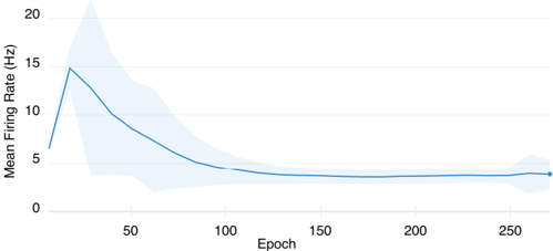
### Visual Description
\n
## Line Chart: Mean Firing Rate vs. Epoch
### Overview
The image presents a line chart illustrating the relationship between "Epoch" on the x-axis and "Mean Firing Rate (Hz)" on the y-axis. A single blue line represents the mean firing rate, with a shaded light blue area indicating the standard deviation or confidence interval around the mean. The chart demonstrates a decreasing trend in mean firing rate as the epoch increases.
### Components/Axes
* **X-axis:** Labeled "Epoch". The scale ranges from approximately 0 to 280, with tick marks at intervals of 50.
* **Y-axis:** Labeled "Mean Firing Rate (Hz)". The scale ranges from approximately 0 to 20, with tick marks at intervals of 5.
* **Data Series:** A single blue line representing the mean firing rate.
* **Confidence Interval:** A light blue shaded area surrounding the blue line, representing the variability or uncertainty in the mean firing rate.
### Detailed Analysis
The blue line starts at approximately 16 Hz at Epoch 0. The line then exhibits a steep downward slope until approximately Epoch 50, where the mean firing rate is around 8 Hz. From Epoch 50 to Epoch 200, the slope becomes less steep, and the mean firing rate gradually decreases to approximately 3 Hz. Between Epoch 200 and Epoch 280, the line plateaus, with the mean firing rate fluctuating around 3 Hz.
Here's a breakdown of approximate data points:
* Epoch 0: ~16 Hz
* Epoch 25: ~12 Hz
* Epoch 50: ~8 Hz
* Epoch 75: ~6 Hz
* Epoch 100: ~5 Hz
* Epoch 150: ~4 Hz
* Epoch 200: ~3.5 Hz
* Epoch 250: ~3.2 Hz
* Epoch 280: ~3.1 Hz
The shaded area (confidence interval) is widest at the beginning of the chart (Epoch 0-50), indicating greater variability in the mean firing rate during this period. As the epoch increases, the shaded area narrows, suggesting a reduction in variability.
### Key Observations
* The mean firing rate decreases significantly during the initial epochs (0-50).
* The rate of decrease slows down after Epoch 50.
* The mean firing rate appears to stabilize around 3 Hz after Epoch 200.
* The confidence interval decreases over time, indicating increasing certainty in the mean firing rate as the epoch progresses.
### Interpretation
This chart likely represents the learning or adaptation process of a neural system or neuron. The decreasing mean firing rate suggests that the system is becoming more efficient or desensitized over time. The initial steep decrease could represent a rapid learning phase, while the subsequent plateau indicates that the system has reached a stable state. The narrowing confidence interval suggests that the system's response becomes more consistent as it learns. This could be observed in a biological neuron adapting to a stimulus, or in an artificial neural network during training. The data suggests a process of habituation or adaptation, where the initial response is strong, but diminishes with repeated exposure. The stabilization at around 3 Hz could represent a baseline level of activity or a point of saturation.
</details>
F igure A. 8 : MSE loss of 50 networks trained with PCM synapses using the mixed-precision method.
<details>
<summary>Image 46 Details</summary>
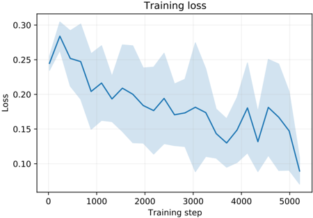
### Visual Description
\n
## Line Chart: Training Loss
### Overview
The image presents a line chart illustrating the training loss over training steps. The chart displays a single blue line representing the average loss, with a shaded light blue area indicating the variance or standard deviation around that average. The chart's purpose is to visualize how well a model is learning during the training process.
### Components/Axes
* **Title:** "Training loss" - positioned at the top-center of the chart.
* **X-axis:** "Training step" - ranging from approximately 0 to 5000, with grid lines.
* **Y-axis:** "Loss" - ranging from approximately 0.10 to 0.30, with grid lines.
* **Data Series:** A single blue line representing the average training loss.
* **Shaded Area:** A light blue shaded region representing the variance around the average loss.
### Detailed Analysis
The blue line representing the average training loss generally slopes downward from left to right, indicating a decreasing loss as the training progresses. The line exhibits fluctuations, showing periods of faster and slower learning.
Here's a breakdown of approximate data points:
* **Step 0:** Loss ≈ 0.28
* **Step 500:** Loss ≈ 0.23
* **Step 1000:** Loss ≈ 0.21
* **Step 1500:** Loss ≈ 0.18
* **Step 2000:** Loss ≈ 0.14
* **Step 2500:** Loss ≈ 0.16
* **Step 3000:** Loss ≈ 0.15
* **Step 3500:** Loss ≈ 0.17
* **Step 4000:** Loss ≈ 0.16
* **Step 4500:** Loss ≈ 0.14
* **Step 5000:** Loss ≈ 0.13
The shaded light blue area varies in width, indicating changes in the standard deviation of the loss. The area is wider at the beginning of training (around step 0-1000) and narrows as training progresses, suggesting that the loss becomes more consistent over time.
### Key Observations
* The training loss decreases overall, indicating that the model is learning.
* The initial phase of training (steps 0-1000) exhibits higher loss and greater variance.
* The loss plateaus somewhat between steps 2000 and 4000, suggesting a slower learning rate.
* The final steps (4000-5000) show a continued decrease in loss, but the magnitude of the decrease is smaller.
### Interpretation
The chart demonstrates a typical learning curve for a machine learning model. The initial high loss and large variance indicate that the model is initially far from optimal and is making significant adjustments. As training progresses, the loss decreases and the variance narrows, indicating that the model is converging towards a more stable and accurate solution. The plateau between steps 2000 and 4000 could suggest that the learning rate needs to be adjusted or that the model is approaching its maximum performance. The continued decrease in loss at the end of training suggests that further training could potentially yield additional improvements, but the diminishing returns may indicate that the model is nearing convergence. The overall trend is positive, suggesting that the training process is effective.
</details>
## supplementary note 6
## appendix 2 : mosaic : in -memory computing and routing for small -world spike -based neuromorphic systems
<details>
<summary>Image 47 Details</summary>
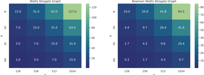
### Visual Description
## Heatmaps: Watts Strogatz and Newman Watts Strogatz Graphs
### Overview
The image presents two heatmaps side-by-side, comparing data for "Watts Strogatz Graph" (left) and "Newman Watts Strogatz Graph" (right). Both heatmaps visualize a relationship between two variables, 'k' and 'n', with color intensity representing a numerical value. Each heatmap has a color scale indicating the mapping between color and value.
### Components/Axes
Both heatmaps share the same axes labels and structure:
* **X-axis:** 'n' with values 128, 256, 512, and 1024.
* **Y-axis:** 'k' with values 8, 16, 32, and 64.
* **Color Scale:** A gradient from dark blue (low values) to light green (high values). The scale ranges from approximately 0 to 130 for the Watts Strogatz Graph and 0 to 85 for the Newman Watts Strogatz Graph.
* **Title:** "Watts Strogatz Graph" (left) and "Newman Watts Strogatz Graph" (right) positioned at the top-center of each heatmap.
### Detailed Analysis or Content Details
**Watts Strogatz Graph (Left Heatmap)**
The heatmap shows increasing values as 'n' increases, and a slight increase as 'k' increases.
* **k = 8:** Values are 15.0 (n=128), 31.0 (n=256), 63.0 (n=512), and 127.0 (n=1024).
* **k = 16:** Values are 7.0 (n=128), 15.0 (n=256), 31.0 (n=512), and 63.0 (n=1024).
* **k = 32:** Values are 3.0 (n=128), 7.0 (n=256), 15.0 (n=512), and 31.0 (n=1024).
* **k = 64:** Values are 3.0 (n=128), 7.0 (n=256), 15.0 (n=512), and 31.0 (n=1024).
**Newman Watts Strogatz Graph (Right Heatmap)**
The heatmap also shows increasing values as 'n' increases, and a slight increase as 'k' increases, but the overall values are lower than the Watts Strogatz Graph.
* **k = 8:** Values are 10.0 (n=128), 20.8 (n=256), 41.8 (n=512), and 84.5 (n=1024).
* **k = 16:** Values are 4.4 (n=128), 9.7 (n=256), 20.4 (n=512), and 41.6 (n=1024).
* **k = 32:** Values are 1.7 (n=128), 4.3 (n=256), 9.6 (n=512), and 20.4 (n=1024).
* **k = 64:** Values are 0.3 (n=128), 1.7 (n=256), 4.3 (n=512), and 9.7 (n=1024).
### Key Observations
* Both graphs exhibit a positive correlation between 'n' and the measured value. As 'n' increases, the value generally increases.
* The Watts Strogatz Graph consistently shows higher values than the Newman Watts Strogatz Graph for the same 'k' and 'n' values.
* The effect of 'k' on the value is less pronounced than the effect of 'n'. Values tend to be relatively stable across different 'k' values for a given 'n'.
* The Newman Watts Strogatz Graph has values that are much closer to zero, especially for lower values of 'n' and higher values of 'k'.
### Interpretation
These heatmaps likely represent some property of network graphs generated using the Watts-Strogatz and Newman-Watts-Strogatz models. 'k' likely represents the average degree of a node (number of connections), and 'n' likely represents the number of nodes in the network. The color intensity represents a metric related to network structure or dynamics, such as clustering coefficient, average path length, or spectral properties.
The higher values in the Watts Strogatz Graph suggest that this model produces networks with stronger structural properties (e.g., higher clustering) or more pronounced dynamics compared to the Newman Watts Strogatz model. The positive correlation between 'n' and the measured value indicates that the property being measured scales with network size. The relatively weak effect of 'k' suggests that the property is less sensitive to the average degree of nodes than to the overall network size.
The difference between the two graphs could be due to the specific algorithms used to generate them, or the parameters used in the algorithms. The Newman Watts Strogatz model may be designed to produce networks with more sparse connections or different topological characteristics. Further investigation would be needed to determine the exact meaning of the measured value and the implications of these differences.
</details>
n
n
F igure A. 9 : The heatmaps show the ratio of zero elements to non-zero elements in the connectivity matrix for two examples of recurrently connected small-world graph generators. As n (number of nodes, e.g., neurons, in the graph) increases and k (number of neighbour nodes for each node in a ring topology) decreases, the more connections in the connectivity matrix will be zero, indicating the increased proportion of non-used memory elements in a n × n crossbar array.
supplementary note 1 Figure A. 9 quantifies the under-utilization of conventional crossbar arrays while storing example small-world connectivity patterns generated by two standard random graph generation models: Watts-Strogatz small-world graphs [ 279 ] and Newman-WattsStrogatz small-world graphs [ 346 ]. The first type of graphs is characterized by a high degree of local clustering with short vertex-vertex distances, observed in neural networks and selforganizing systems, whereas the latter type mostly captures the properties of lattices associated with statistical physics.
supplementary note 2 To communicate the events between the computing nodes in neuromorphic chips, AER communication scheme has been developed and used [ 308 ]. In AER, whenever a spiking neuron in a chip (or module) generates a spike, its 'address' (or any given ID) is written on a high-speed digital bus and sent to the receiving neuron(s) in one (or more) receiver module(s). In general, AER processing modules require at least one AER input port and one AER output port. As neuromorphic systems scale up in size, complexity, and functionality, researchers have been developing more complex and smarter AER 'variations' to maintain the efficiency, reconfigurability, and reliability of the ever-growing target systems they want to build. The scheme that is used to transport events can be source or destination based, where the source or destination address is embedded in the sent event 'packet'. In the source-based scheme, each receiving neuron has a local CAM that stores the address of all the neurons that are connected to it. In the destination-based approach, each event hops between the nodes where its address gets compared to the node's address until it matches and thus gets delivered. Source-driven routing provides the designer with more freedom to balance event traffic and design routes, but the hardware complexity increases the delays. Destination-based creates pre-determined routes along the network and the designer can only change the output ports [ 347 ]. In summary, in source-based routing, the system requires a CAM memory per neuron, which results in an increase in the area and memory access read times. In destination-based routing, the configurability in the network structure is reduced. Comparatively, in the Mosaic, the routers are memory crossbars that are distributed between the computing cores and steer the spiking information in the mesh. Thus, neither local CAMs, nor a centralized memory is required for routing.
F igure A. 10 : (top) Different random graphs generated using Mosaic model, changing the probability of devices being in their High Conductive state in the neuron tile ( pn ) and routing tile ( pr ). (bottom) The probability of device switching is a function of the voltage applied to it while being programmed.
<details>
<summary>Image 48 Details</summary>
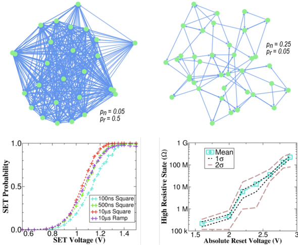
### Visual Description
## Network Diagrams & Charts: Memristor Network Performance
### Overview
The image presents a combination of network diagrams illustrating memristor network configurations and two charts detailing the performance characteristics of these networks. The diagrams show connectivity patterns with associated probabilities, while the charts depict SET probability versus SET voltage and high resistive state versus absolute reset voltage.
### Components/Axes
**Network Diagrams:**
* **Nodes:** Represented by green circles.
* **Connections:** Represented by light blue lines.
* **Labels:** `pn = 0.05`, `pr = 0.5` (left diagram); `pn = 0.25`, `pr = 0.05` (right diagram). These likely represent the probability of a node being 'on' (pn) and the probability of a connection existing (pr).
**Chart 1: SET Probability vs. SET Voltage**
* **X-axis:** SET Voltage (V), ranging from approximately 0.6 to 1.45 V.
* **Y-axis:** SET Probability, ranging from approximately 0.0 to 1.0.
* **Data Series:**
* 100ns Square (cyan 'x' markers)
* 500ns Square (green '+' markers)
* 10µs Square (light blue '*' markers)
* 10µs Ramp (purple diamond markers)
**Chart 2: High Resistive State vs. Absolute Reset Voltage**
* **X-axis:** Absolute Reset Voltage (V), ranging from approximately 1.5 to 3.0 V.
* **Y-axis:** High Resistive State (Ω), on a logarithmic scale ranging from 100 kΩ to 100 MΩ.
* **Legend:**
* Mean (solid black line)
* 1σ (dashed cyan line)
* 2σ (dashed-dotted brown line)
### Detailed Analysis or Content Details
**Network Diagrams:**
The left diagram shows a denser network with `pn = 0.05` and `pr = 0.5`. The right diagram shows a sparser network with `pn = 0.25` and `pr = 0.05`. The diagrams visually represent the connectivity of the memristor network.
**Chart 1: SET Probability vs. SET Voltage**
* **100ns Square:** The SET probability increases rapidly between approximately 0.8V and 1.1V, reaching near 1.0 by 1.2V.
* **500ns Square:** The SET probability increases more gradually than the 100ns Square, starting to increase noticeably around 0.9V and reaching near 1.0 by 1.3V.
* **10µs Square:** The SET probability increases very gradually, starting to increase around 1.0V and reaching near 1.0 by 1.4V.
* **10µs Ramp:** The SET probability increases rapidly, similar to the 100ns Square, starting around 0.75V and reaching near 1.0 by 1.2V.
**Chart 2: High Resistive State vs. Absolute Reset Voltage**
* **Mean:** The mean high resistive state increases rapidly between approximately 1.7V and 2.2V, then increases more slowly until 3.0V, reaching approximately 80 MΩ.
* **1σ:** The 1σ curve starts at approximately 200 kΩ at 1.5V, increases rapidly to approximately 1 MΩ at 2.0V, and then increases more slowly to approximately 20 MΩ at 3.0V.
* **2σ:** The 2σ curve starts at approximately 100 kΩ at 1.5V, increases rapidly to approximately 500 kΩ at 2.0V, and then increases more slowly to approximately 5 MΩ at 3.0V.
### Key Observations
* Shorter pulse durations (100ns, 500ns) for the square wave exhibit faster SET probabilities compared to the longer 10µs square wave.
* The 10µs ramp waveform shows a SET probability curve similar to the 100ns square wave.
* The high resistive state increases significantly with increasing reset voltage.
* The 1σ and 2σ curves show the variability in the high resistive state, with the spread increasing with reset voltage.
### Interpretation
The data suggests that the SET probability is highly dependent on the pulse duration and waveform shape. Shorter pulses and ramp waveforms are more effective at setting the memristors. The high resistive state is also strongly influenced by the reset voltage, with higher voltages leading to higher resistance. The spread in the high resistive state (represented by 1σ and 2σ) indicates the inherent variability in the memristor devices.
The network diagrams show how the connectivity of the network can be controlled by adjusting the probabilities of node activation (`pn`) and connection formation (`pr`). The denser network (left diagram) with `pr = 0.5` likely exhibits different behavior than the sparser network (right diagram) with `pr = 0.05`. The combination of network topology and device characteristics (SET/Reset behavior) is crucial for designing and optimizing memristor-based systems. The charts provide insights into the electrical characteristics of the memristors, which are essential for understanding and predicting the behavior of the network. The logarithmic scale on the Y-axis of the second chart highlights the large dynamic range of the memristor's resistance.
</details>
F igure A. 11 : Mosaic connectivity example, formed by setting the probability of connection within Neuron Tile ( pNT ) and Routing Tiles ( pRT ). (left) Densely connected Mosaic composed of 2 Neuron Tiles and 1 Routing Tile. The graph related to its connectivity is shown as well adjacency matrix. (right) Sparsely connected Mosaic. The graph is programmed to favor the intraNeuton Tile connectivity and allow for two clusters to emerge, penalizing connections between the two clusters.
<details>
<summary>Image 49 Details</summary>
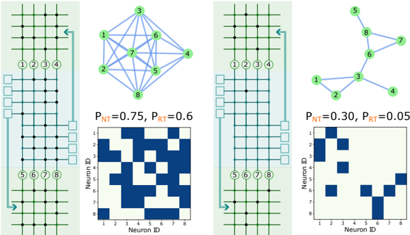
### Visual Description
\n
## Diagram: Neural Network Connectivity and Activity
### Overview
The image presents a comparison of two neural network configurations with differing connectivity probabilities and resulting activity patterns. It consists of four panels arranged in two columns. Each panel shows a grid-like representation of neurons, a corresponding network graph, and a heatmap representing neuron activity.
### Components/Axes
Each panel contains the following components:
* **Neuron Grid:** A grid of squares representing neurons, with numbered circles indicating specific neurons. Arrows indicate input and output connections.
* **Network Graph:** A graph depicting the connections between neurons. Nodes represent neurons, and edges represent connections.
* **Heatmap:** A square matrix representing the activity level between neurons. The x and y axes are labeled "Neuron ID". The color intensity indicates the strength of the connection or activity.
* **Probability Labels:** Each panel includes labels indicating the values of P<sub>NT</sub> and P<sub>RT</sub>.
### Detailed Analysis or Content Details
**Panel 1 (Left Column)**
* **Neuron Grid:** 8 neurons are numbered 1 through 8. Input arrows point to neurons 1-4, and output arrows originate from neurons 5-8.
* **Network Graph:** A fully connected graph with 8 nodes (neurons). Every neuron is connected to every other neuron.
* **Probability Labels:** P<sub>NT</sub> = 0.75, P<sub>RT</sub> = 0.6
* **Heatmap:** The heatmap is an 8x8 matrix. The color intensity is variable, with darker blue indicating higher activity. Notable activity is observed at:
* (1,1) - Moderate intensity
* (1,2) - Moderate intensity
* (1,3) - Moderate intensity
* (1,4) - Moderate intensity
* (2,1) - Moderate intensity
* (2,2) - Moderate intensity
* (2,3) - Moderate intensity
* (2,4) - Moderate intensity
* (3,1) - Moderate intensity
* (3,2) - Moderate intensity
* (3,3) - Moderate intensity
* (3,4) - Moderate intensity
* (4,1) - Moderate intensity
* (4,2) - Moderate intensity
* (4,3) - Moderate intensity
* (4,4) - Moderate intensity
* (5,5) - Moderate intensity
* (5,6) - Moderate intensity
* (5,7) - Moderate intensity
* (5,8) - Moderate intensity
* (6,5) - Moderate intensity
* (6,6) - Moderate intensity
* (6,7) - Moderate intensity
* (6,8) - Moderate intensity
* (7,5) - Moderate intensity
* (7,6) - Moderate intensity
* (7,7) - Moderate intensity
* (7,8) - Moderate intensity
* (8,5) - Moderate intensity
* (8,6) - Moderate intensity
* (8,7) - Moderate intensity
* (8,8) - Moderate intensity
**Panel 2 (Right Column)**
* **Neuron Grid:** Similar to Panel 1, with 8 neurons numbered 1 through 8.
* **Network Graph:** A sparsely connected graph with 8 nodes. Neurons 1, 2, 3, and 4 form a connected cluster, and neurons 5, 6, 7, and 8 form another connected cluster. There are limited connections between the two clusters.
* **Probability Labels:** P<sub>NT</sub> = 0.30, P<sub>RT</sub> = 0.05
* **Heatmap:** The heatmap is an 8x8 matrix. The color intensity is significantly lower than in Panel 1, indicating lower activity. Notable activity is observed at:
* (1,2) - Low intensity
* (2,1) - Low intensity
* (2,3) - Low intensity
* (3,2) - Low intensity
* (5,6) - Low intensity
* (6,5) - Low intensity
* (6,7) - Low intensity
* (7,6) - Low intensity
### Key Observations
* **Connectivity vs. Activity:** Panel 1, with higher connectivity probabilities (P<sub>NT</sub> = 0.75, P<sub>RT</sub> = 0.6), exhibits significantly higher overall activity in the heatmap compared to Panel 2 (P<sub>NT</sub> = 0.30, P<sub>RT</sub> = 0.05).
* **Network Structure and Activity Patterns:** The fully connected network in Panel 1 shows a more uniform distribution of activity across all neurons. The sparsely connected network in Panel 2 shows activity concentrated within the two clusters.
* **Heatmap Intensity:** The heatmap in Panel 1 has a much wider range of color intensities, indicating a more diverse range of activity levels.
### Interpretation
The diagram illustrates the relationship between network connectivity, connection probabilities, and resulting neural activity. The higher connectivity probabilities in Panel 1 lead to a more densely connected network and, consequently, higher overall activity. The heatmap visually represents this, showing a greater number of active connections.
Panel 2 demonstrates that lower connectivity probabilities result in a sparser network and reduced activity. The activity is localized within the two clusters, suggesting that information processing is more compartmentalized.
The values of P<sub>NT</sub> and P<sub>RT</sub> likely represent the probabilities of creating new connections (NT - New Transmission) and retaining existing connections (RT). The difference in these probabilities significantly impacts the network's structure and function.
The diagram suggests that network connectivity is a crucial factor in determining the level and distribution of neural activity. This has implications for understanding how neural networks learn, process information, and adapt to changing environments. The diagram is a simplified representation, but it effectively conveys the fundamental principles of neural network dynamics.
</details>
supplementary note 3 Routing tiles define the connectivity of spiking neural networks implemented on Mosaic. When the number of memristive devices in the routing tiles which are in their high-conductive state (HCS) is not sparse, Mosaic resembles a densely connected neural network (Fig. A. 10 , top left). When most of the memristor in the routing tiles are in the low-conductance state, Mosaic is sparsely connected (Fig. A. 10 , top right). Furthermore, one can further sparsify Mosaic networks by setting memristors in the neuron tiles to the LCS. To do so, we can change the probability of memristors being in their HCS in the neuron tiles, pn , and in the
routing tiles, pr . The switching of the RRAMs presents the property of probabilistic switching as a function of the voltage applied during the programming operation as is shown in Fig. A. 10 , bottom.
Fig. A. 11 shows the construction of two graph topologies, made of 2 Neuron Tiles and one Routing Tile, to clarify the formation of the graphical structure in the Mosaic. By controlling the probability of connections within the Neuron and Routing Tiles, we can produce a densely connected graph (left) with pNT = 0.75, pRT = 0.6, and a sparse graph (right) with pNT = 0.30, pRT = 0.05.
The corresponding connectivity matrix is also shown in the figure, which is directly represented as a hardware architecture in the 3 tiles of the Mosaic, as shown in the figure.
F igure A. 12 : (Neuron tiles (green) transfer information in the form of spikes to each other through routing tiles (blue). Details of the Mosaic architecture is shown with the size of the neuron and routing tiles. The neuron tiles receive feed-forward input from four directions of North (N), East (E), West (W), and South (S), and local recurrent input from the neurons in the tile. The neurons integrate the information and once spike, send their output to 4 directions. Having 4 neurons in a tile, gives rise to 16 outputs ( 4 outputs copied in 4 directions), and 20 inputs ( 4 inputs from 4 directions ( 16 ), plus 4 recurrent inputs). The routing tiles receive 16 inputs ( 4 inputs from 4 directions) and send out 16 outputs ( 4 outputs in 4 directions). In the crossbars, the red squares and black squares represent devices in their high conductive and low conductive state, respectively. The connection between the neuron tile and the routing tile is directly through a wire. For instance, V out < 3:0 > is the same as the Vin , W , and V in,E < 3:0 > is the same as Vout , W .
<details>
<summary>Image 50 Details</summary>
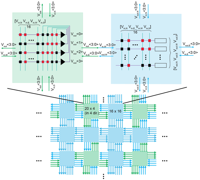
### Visual Description
\n
## Diagram: Interconnect of Voltage Sources and Rectangular Array
### Overview
The image depicts a schematic diagram illustrating the interconnection of multiple voltage sources to a rectangular array of elements. The diagram shows a hierarchical structure, starting with individual voltage sources, then a grouping of these sources, and finally their connection to a grid-like array. The diagram appears to represent a power distribution or signal routing scheme.
### Components/Axes
The diagram consists of the following key components:
* **Voltage Sources:** Represented by triangular symbols with input and output terminals labeled with voltage notations (e.g., V<sub>in,N</sub>, V<sub>out</sub>).
* **Interconnections:** Horizontal and vertical lines connecting the voltage sources to the rectangular array. These lines represent electrical connections.
* **Rectangular Array:** A grid of rectangular blocks, presumably representing individual elements or components.
* **Labels:** Various labels indicating voltage names and array dimensions.
* **Ellipsis (...):** Used to indicate continuation of patterns.
The diagram does not have traditional axes like a chart. Instead, it uses spatial arrangement to convey information.
### Detailed Analysis or Content Details
**Top Section (Voltage Source Grouping):**
* A group of voltage sources is shown on the left. Each source has an input (V<sub>in,N</sub>) and an output (V<sub>out</sub>). The subscript 'N' likely denotes a specific source within the group. The voltage notation "<3:0>" appears next to the voltage labels, suggesting a bit width or range of values.
* The voltage sources are connected in a parallel arrangement.
* The grouping is repeated multiple times, indicated by the ellipsis.
* The right side shows a similar grouping, with labels V<sub>in,E</sub>, V<sub>in,S</sub>, V<sub>in,W</sub>, V<sub>out,E</sub>, V<sub>out,S</sub>, V<sub>out,W</sub>. The subscripts E, S, W, and N likely denote East, South, West, and North directions.
* There are labels V<sub><0>out</sub>, V<sub><1>out</sub>, V<sub><2>out</sub>, V<sub><3>out</sub>.
**Bottom Section (Rectangular Array):**
* The rectangular array is composed of multiple blocks.
* The array is labeled "20 x 4 (in dir.)" and "16 x 16". This indicates the dimensions of the array. The "(in dir.)" suggests the 20x4 array is oriented in a specific direction.
* Green arrows point towards the array, representing the input voltages.
* The array is also repeated multiple times, indicated by the ellipsis.
* The output of the array is labeled "out".
**Interconnections:**
* The voltage sources are connected to the array via horizontal and vertical lines.
* The lines are colored red, indicating electrical connections.
* The green arrows represent the direction of voltage flow.
### Key Observations
* The diagram shows a structured approach to distributing voltage to a large array of elements.
* The use of multiple voltage sources suggests a need for redundancy or increased power capacity.
* The array dimensions indicate a significant number of elements.
* The "<3:0>" notation suggests a digital or quantized voltage representation.
* The diagram is highly symmetrical, suggesting a regular pattern of connections.
### Interpretation
The diagram likely represents a power distribution network for an integrated circuit or a similar electronic system. The voltage sources provide power to the rectangular array, which could represent a memory array, a display, or a processing unit. The hierarchical structure allows for efficient distribution of power to a large number of elements. The "<3:0>" notation suggests that the voltages are controlled with a resolution of 4 bits. The symmetry of the diagram indicates a regular and predictable layout, which is common in integrated circuit design. The use of directional labels (N, S, E, W) suggests that the array may have specific orientation requirements. The diagram is a high-level representation and does not provide details about the specific components or their functionality. It focuses on the interconnection scheme and the overall architecture of the system. The ellipsis indicate that the array and voltage source groupings are repeated, suggesting a scalable design.
</details>
supplementary note 4 Figure A. 12 shows the details of the Mosaic architecture, with a zoomed in neuron and routing tile pair. The diagram in the top shows how one cluster of neuron/one router sends and receives information to and from the routing/neuron tile. This
highlights the strength of this architecture which makes the connectivity easy through simple wiring to the neighbour, without suffering from long wires, as the maximum length of a wire is the size of the wire from one row/column, plus the size of the connecting column/row.
F igure A. 13 : Schematic of the neuron tile including the CMOS synapse and neuron circuits fabricated for use in this paper. RRAMs are used as the weights of the neurons. On the arrival of any of the input events Vin < i > , the amplifier pins node Vx to Vtop and thus a read voltage equivalent to Vtop -Vbot is applied across Gi , giving rise to current i in at M 1 . This current is mirrored to M 2 giving rise to i buf f which is in turn again mirrored through the M 3 -M 4 transistor pair. The 'synaptic dynamics' circuit is the Differential Pair Integrator (DPI) [ 311 ]. On the arrival of any of the input events, Vi , 0 < i < n , Iw , equivalent to i buf f , flows in transistor M 5. Depending on the value on Vg , a portion of Iw flows out of the MOS capacitor M 6 and discharges it. This current is proportional to Gi , 0 < i < n . As soon as the event is gone, MOS capacitor M 6 charges back through the M 8 path with current Itau , which determines the rate of charging, and thus the time constant of the synaptic dynamics. The output current of the DPI synapse, Isyn , is injected into the neuron's membrane potential node, Vmem , and charges MOS capacitor M 13 . There is also an alternative path with a DC current input through M 17 which can charge neuron's membrane potential. Membrane potential charging has a time constant determined by Vlk at the gate of M 11 . As soon as the voltage developed on Vmem passes the threshold of the following inverter stage, it generates a pulse. The width of the pulse, depends on the delay of the feedback path from Vout to the gate of M 12 . This delay is determined by the inverter delays, and the refractory time constant. The inverter symbols with the horizontal dashed lines correspond to a starved inverter circuits with longer delays. The refractory period time constant depends on the MOS cap M 16 and the bias on Vrp .
<details>
<summary>Image 51 Details</summary>
### Visual Description
\n
## Diagram: Operational Amplifier Circuit
### Overview
The image depicts a schematic diagram of an operational amplifier (op-amp) circuit, likely a component within a larger analog system. The diagram shows a series of transistors and other components arranged to perform amplification and signal processing. The circuit is divided into several functional blocks, including an input stage, a gain stage, and an output stage.
### Components/Axes
The diagram does not contain axes or scales in the traditional sense of a chart. Instead, it uses standard electronic schematic symbols to represent components. Key labels include:
* **V**: Represents a voltage source.
* **G**: Represents a gate terminal of a transistor.
* **V<sub>bot</sub>**: Bottom voltage.
* **V<sub>top</sub>**: Top voltage.
* **i**: Input current.
* **M1-M16**: Transistor identifiers.
* **V<sub>buff</sub>**: Buffer voltage.
* **V<sub>mem</sub>**: Memory voltage.
* **V<sub>out</sub>**: Output voltage.
* **V<sub>dc</sub>**: DC voltage.
* **V<sub>in</sub>**: Input voltage.
* **<V<sub>th</sub>>**: Threshold voltage.
* The diagram also includes symbols for an op-amp (triangle), and voltage sources (circles).
### Detailed Analysis / Content Details
The circuit can be broken down into the following sections:
1. **Input Stage (Leftmost):** This section consists of several transistors (M1-M?) connected in a differential amplifier configuration. The input voltage 'V' is applied to the gates of these transistors. The bottom voltage 'V<sub>bot</sub>' and top voltage 'V<sub>top</sub>' are also connected to the transistors. The input current 'i' is indicated.
2. **Buffer Stage (Green Box):** A single transistor (M3) is shown as a buffer, with 'V<sub>buff</sub>' as its output. The buffer receives input from the op-amp symbol.
3. **Gain Stage (Center):** This section contains a series of transistors (M4-M9) and logic gates (an OR gate). The input to this stage comes from the buffer. The threshold voltage '<V<sub>th</sub>>' is also present in this section.
4. **Output Stage (Blue Box):** This section consists of several transistors (M10-M16) and appears to be a current mirror or similar output driver configuration. The output voltage 'V<sub>out</sub>' is indicated. The DC voltage 'V<sub>dc</sub>' is also present. The output stage also contains multiple inverters (represented by triangles).
The diagram shows connections between these stages, indicating the flow of signal through the circuit. The ground symbol is present throughout the diagram.
### Key Observations
* The circuit appears to be designed for low-voltage operation, as indicated by the 'V<sub>bot</sub>' and 'V<sub>top</sub>' labels.
* The use of multiple transistors in the input stage suggests a differential amplifier configuration, which is common in op-amp designs.
* The buffer stage likely isolates the input stage from the gain stage, preventing loading effects.
* The output stage is designed to provide a low-impedance output, capable of driving a load.
### Interpretation
This diagram represents a complex analog circuit, likely a low-voltage operational amplifier. The circuit is designed to amplify a small input voltage 'V' and produce a larger output voltage 'V<sub>out</sub>'. The differential input stage provides common-mode rejection, while the buffer stage isolates the input from the gain stage. The gain stage provides the desired amplification, and the output stage drives the load. The presence of the threshold voltage '<V<sub>th</sub>>' suggests that the circuit may incorporate some form of threshold detection or switching behavior. The overall design suggests a focus on precision and low-power operation. The circuit is likely part of a larger system, such as a data converter, sensor interface, or control loop. The diagram does not provide specific numerical values for component parameters or performance characteristics, but it does provide a clear overview of the circuit's architecture and functionality.
</details>
F igure A. 14 : Measurements from fabricated neuron's output frequency as a function of the input DC voltage. The DC voltage is applied at the gate of transistor M 17 shown in Fig. A. 13 as Vdc . Therefore, as the gate voltage of M 17 changes linearly, the current of M 17 and thus the output frequency of the neuron changes non-linearly. Each curve is measured with a different neuron's time constant, determined by a different voltage, Vlk , on the gate of transistor M 11 in Fig. A. 13 . As the leak voltage increases, the neuron's time constant decreases, giving rise to a lower output frequency.
<details>
<summary>Image 52 Details</summary>
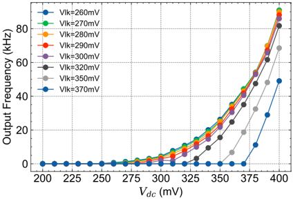
### Visual Description
\n
## Chart: Output Frequency vs. DC Voltage
### Overview
The image presents a line chart illustrating the relationship between Output Frequency (in kHz) and DC Voltage (Vdc, in mV) for various values of Vik (in mV). The chart displays seven different curves, each representing a constant Vik value, showing how the output frequency changes with varying DC voltage.
### Components/Axes
* **X-axis:** Vdc (mV), ranging from approximately 200 mV to 400 mV. The axis is labeled "Vdc (mV)".
* **Y-axis:** Output Frequency (kHz), ranging from 0 kHz to 80 kHz. The axis is labeled "Output Frequency (kHz)".
* **Legend:** Located at the top-left corner of the chart. It identifies each line with its corresponding Vik value:
* Blue: Vik = 260 mV
* Green: Vik = 270 mV
* Orange: Vik = 280 mV
* Red: Vik = 290 mV
* Purple: Vik = 300 mV
* Black: Vik = 320 mV
* Gray: Vik = 350 mV
* Dark Blue: Vik = 370 mV
### Detailed Analysis
The chart shows a non-linear relationship between Vdc and Output Frequency for each Vik value. The output frequency remains close to zero for Vdc values below approximately 300 mV, then increases rapidly as Vdc increases beyond this point.
Here's a breakdown of the data points, with approximate values based on visual inspection:
* **Vik = 260 mV (Blue):** The line starts at approximately (200 mV, 0 kHz) and remains near zero until around 360 mV. It then rises steeply, reaching approximately (400 mV, 12 kHz).
* **Vik = 270 mV (Green):** Starts at approximately (200 mV, 0 kHz). Rises more quickly than the 260mV line, reaching approximately (400 mV, 20 kHz).
* **Vik = 280 mV (Orange):** Starts at approximately (200 mV, 0 kHz). Rises more quickly than the 270mV line, reaching approximately (400 mV, 30 kHz).
* **Vik = 290 mV (Red):** Starts at approximately (200 mV, 0 kHz). Rises more quickly than the 280mV line, reaching approximately (400 mV, 45 kHz).
* **Vik = 300 mV (Purple):** Starts at approximately (200 mV, 0 kHz). Rises more quickly than the 290mV line, reaching approximately (400 mV, 55 kHz).
* **Vik = 320 mV (Black):** Starts at approximately (200 mV, 0 kHz). Rises more quickly than the 300mV line, reaching approximately (400 mV, 70 kHz).
* **Vik = 350 mV (Gray):** Starts at approximately (200 mV, 0 kHz). Rises more quickly than the 320mV line, reaching approximately (400 mV, 75 kHz).
* **Vik = 370 mV (Dark Blue):** Starts at approximately (200 mV, 0 kHz). Rises more quickly than the 350mV line, reaching approximately (400 mV, 80 kHz).
All lines exhibit a similar trend: a relatively flat response at low Vdc values, followed by a steep increase in output frequency as Vdc increases. The higher the Vik value, the higher the output frequency for a given Vdc value above the threshold.
### Key Observations
* The output frequency is highly sensitive to changes in Vdc above approximately 300 mV.
* Increasing Vik results in a higher output frequency for a given Vdc.
* The curves are not perfectly symmetrical; the rate of increase in frequency is steeper at higher Vdc values.
* There is a clear threshold effect, where the output frequency remains near zero until Vdc reaches a certain level.
### Interpretation
This chart likely represents the characteristics of an oscillator circuit or a similar electronic device where the output frequency is dependent on both the DC bias voltage (Vdc) and a control voltage (Vik). The data suggests that the device has a turn-on voltage (around 300 mV) below which it does not oscillate. The Vik parameter appears to control the gain or sensitivity of the oscillator, with higher Vik values leading to a more pronounced frequency response to changes in Vdc.
The steep increase in frequency at higher Vdc values indicates a non-linear relationship, potentially due to the characteristics of the active components within the circuit. The curves could be used to design or analyze circuits that require a voltage-controlled oscillator with specific frequency characteristics. The data could also be used to identify potential operating regions where the device is most stable or sensitive.
</details>
supplementary note 5 Details of the implementation of the neuron row, the circuit that leverages the information of the conductance of a memristor to weight the effect of a spike to a neuron is shown in Figure A. 13 . The circuit features multiple inputs connected to a row of memristive devices (left) and a Front-End circuit buffering the current read from the devices to a differential-pair-integrator synapse. The synapse is then connected to a leaky-integrated-and-fire (LIF) neuron which eventually emits a spike. Figure A. 14 delves deeper in the behavior of the LIF neuron analyzing its output spiking frequency against an input DC voltage and its linear behavior respect to the RRAM conductance in a neuron row circuit.
T
F igure A. 15 : Schematic of a routing tile circuit offering two paths per direction. The routing tile receives eight inputs, comprising two pulse channels per direction, labelled as < 0 > or < 1 >, from the neighbouring tiles to the North (N), South (S), East (E) and West (W), and provides complimentary outputs. An example is shown of an input pulse arriving to the common gate of the fourth row of memory. Devices are coloured green or red to denote whether they are in the HCS or LCS. It is shown that, due to this input pulse, output pulses are produced by the routing columns containing the (green) devices programmed in the HCS.
<details>
<summary>Image 53 Details</summary>
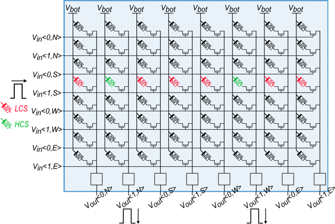
### Visual Description
## Diagram: State Transition Diagram for a Circuit
### Overview
The image depicts a state transition diagram for a circuit, likely a sequential logic circuit. It shows the behavior of the circuit under different input conditions, represented by various combinations of Vin (Input Voltage) and Vout (Output Voltage). The diagram is organized as a grid, with input states along the vertical axis and output states along the horizontal axis. Each cell in the grid represents a possible state transition, indicated by the presence of a transistor symbol and a color-coded marker.
### Components/Axes
* **Vertical Axis (Input States):** Represents the input conditions, labeled as follows:
* Vin < 0, N> (approximately -0.2V, Negative)
* Vin < 1, N> (approximately 0.8V, Negative)
* Vin < 0, S> (approximately -0.2V, Slow)
* Vin < 1, S> (approximately 0.8V, Slow)
* LCS Vin < 0, W> (approximately -0.2V, Weak)
* HCS Vin < 1, W> (approximately 0.8V, Weak)
* Vin < 0, E> (approximately -0.2V, Early)
* Vin < 1, E> (approximately 0.8V, Early)
* **Horizontal Axis (Output States):** Represents the output conditions, labeled as follows:
* Vout < 0, N> (approximately -0.2V, Negative)
* Vout < 1, N> (approximately 0.8V, Negative)
* Vout < 0, S> (approximately -0.2V, Slow)
* Vout < 1, S> (approximately 0.8V, Slow)
* Vout < 0, W> (approximately -0.2V, Weak)
* Vout < 1, W> (approximately 0.8V, Weak)
* Vout < 0, E> (approximately -0.2V, Early)
* Vout < 1, E> (approximately 0.8V, Early)
* **Legend:**
* Red markers (LCS): Represent a Low Current State.
* Green markers (HCS): Represent a High Current State.
* **Top Row:** Labeled "Vbot" repeated across all columns.
* **Bottom Row:** Shows waveform symbols representing Vout, with alternating positive and negative pulses.
* **Left Column:** Shows waveform symbols representing Vin, with alternating positive and negative pulses.
### Detailed Analysis
The diagram consists of an 8x8 grid. Each cell contains a transistor symbol, and some cells also contain a colored marker (red or green). The presence of a marker indicates a specific current state (LCS or HCS).
* **Vin < 0, N> Row:** Most cells in this row are marked with red (LCS) markers. Vout < 1, N> and Vout < 1, S> have green (HCS) markers.
* **Vin < 1, N> Row:** Most cells are marked with red (LCS) markers. Vout < 1, N> and Vout < 1, S> have green (HCS) markers.
* **Vin < 0, S> Row:** Most cells are marked with red (LCS) markers. Vout < 1, N> and Vout < 1, S> have green (HCS) markers.
* **Vin < 1, S> Row:** Most cells are marked with red (LCS) markers. Vout < 1, N> and Vout < 1, S> have green (HCS) markers.
* **LCS Vin < 0, W> Row:** Most cells are marked with red (LCS) markers. Vout < 1, N> and Vout < 1, S> have green (HCS) markers.
* **HCS Vin < 1, W> Row:** Most cells are marked with red (LCS) markers. Vout < 1, N> and Vout < 1, S> have green (HCS) markers.
* **Vin < 0, E> Row:** Most cells are marked with red (LCS) markers. Vout < 1, N> and Vout < 1, S> have green (HCS) markers.
* **Vin < 1, E> Row:** Most cells are marked with red (LCS) markers. Vout < 1, N> and Vout < 1, S> have green (HCS) markers.
The transistor symbols within each cell appear consistent, suggesting a similar circuit configuration for each state transition.
### Key Observations
* The majority of state transitions result in a Low Current State (LCS), indicated by the prevalence of red markers.
* Transitions to a High Current State (HCS) are more likely when Vout is < 1, N or < 1, S.
* The diagram suggests a strong dependency between input and output voltage levels and the resulting current state.
* The "Vbot" label at the top of the diagram is unclear in its function without further context.
### Interpretation
This diagram likely represents the behavior of a digital circuit, possibly a latch or a flip-flop. The input voltage (Vin) and output voltage (Vout) define the current state of the circuit, and the colored markers indicate whether the circuit is in a Low Current State (LCS) or a High Current State (HCS). The diagram demonstrates how the circuit transitions between these states based on the input conditions.
The consistent transistor symbol across all cells suggests a uniform circuit structure, while the varying current states indicate different operating modes. The prevalence of LCS suggests that the circuit is designed to minimize power consumption in most states. The specific meaning of "N", "S", "W", and "E" in the voltage labels is unclear without additional context, but they likely represent different operating conditions or timing phases. The "Vbot" label could refer to a bottom voltage rail or a reference voltage.
The diagram provides a visual representation of the circuit's state machine, allowing engineers to analyze its behavior and identify potential design flaws. The clear distinction between LCS and HCS states is crucial for understanding the circuit's functionality and performance.
</details>
F igure A. 16 : The routing column circuit with example waveforms. Input (red, left) voltage pulses, Vin, draw a current iin proportional to the conductance state, Gn, of the read 1 T 1 R structures. Two devices are labelled with HCS, indicating that they have been programmed with a conductance corresponding to the high conductance state, and one is labelled LCS in reference to the low conductance state. This resulting currents are buffered (green, centre), ibuff , into a current comparator circuit where it is compared with a reference current iref . When the buffered current exceeds the reference current a voltage pulse is generated at the column output (blue, right).
<details>
<summary>Image 54 Details</summary>
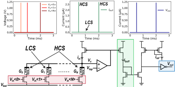
### Visual Description
\n
## Diagram: Circuit and Signal Waveforms
### Overview
The image presents a schematic diagram of a circuit, likely an amplifier or comparator, alongside three time-domain signal waveforms. The circuit appears to be a multi-stage amplifier with a Low-Current Switching (LCS) input and a High-Current Steering (HCS) output. The waveforms show the input voltages (V<sub>in</sub>), input current (i<sub>in</sub>), and output current (V<sub>out</sub>) over time.
### Components/Axes
The diagram consists of the following key components:
* **LCS Block:** A series of transistors (G<sub>0</sub> to G<sub>N</sub>) connected to input voltages V<sub>in</sub><0>, V<sub>in</sub><1>, and V<sub>in</sub><N>, and a bottom voltage V<sub>bot</sub>.
* **HCS Block:** Indicates the high-current steering section.
* **Operational Amplifier (Op-Amp):** A standard Op-Amp symbol with inputs V<sub>x</sub> and V<sub>top</sub>.
* **Buffer Stage:** A transistor-based buffer circuit.
* **Output Stage:** A transistor-based output stage.
* **Waveform Plots:** Three plots showing voltage and current signals over time.
* **Plot 1 (Left):** Voltage vs. Time, with axes labeled "Voltage (V)" and "Time (ms)". Includes three lines: V<sub>in</sub><0>, V<sub>in</sub><1>, and V<sub>in</sub><N>.
* **Plot 2 (Center):** Current vs. Time, with axes labeled "Current (µA)" and "Time (ms)". Includes a single line: i<sub>buff</sub>.
* **Plot 3 (Right):** Current vs. Time, with axes labeled "Current (µA)" and "Time (ms)". Includes a single line: V<sub>out</sub>.
### Detailed Analysis or Content Details
**Waveform Analysis:**
* **V<sub>in</sub><0>, V<sub>in</sub><1>, V<sub>in</sub><N> (Left Plot):** These three voltage waveforms are pulsed. Each pulse rises to approximately 1.25V and falls to 0V. The pulses are spaced approximately 1ms apart, with the first pulse starting at 0ms, the second at 1ms, and the third at 2ms. The lines are colored blue, red, and black respectively.
* **i<sub>buff</sub> (Center Plot):** This current waveform is approximately constant at 0.25 µA for the entire 3ms duration. The line is colored green.
* **V<sub>out</sub> (Right Plot):** This current waveform is pulsed, similar to the input voltages. Each pulse rises to approximately 1.25 µA and falls to 0 µA. The pulses are spaced approximately 1ms apart, with the first pulse starting at 0ms, the second at 1ms, and the third at 2ms. The line is colored blue.
**Circuit Analysis:**
* The LCS block appears to be a series of transistors acting as switches, controlled by the input voltages V<sub>in</sub><0>, V<sub>in</sub><1>, and V<sub>in</sub><N>.
* The HCS block receives input from the Op-Amp and steers current based on the amplified signal.
* The buffer stage likely provides impedance matching and isolation between the Op-Amp output and the output stage.
* The output stage appears to be a current source or current mirror, providing a controlled output current.
* The text "LCS" and "HCS" are explicitly labeled, pointing to the respective blocks.
* The input current to the Op-Amp is labeled "i<sub>in</sub>".
* The output voltage is labeled "V<sub>out</sub>".
* The input voltages to the Op-Amp are labeled "V<sub>x</sub>" and "V<sub>top</sub>".
* The bottom voltage is labeled "V<sub>bot</sub>".
### Key Observations
* The input voltages (V<sub>in</sub>) are pulsed, and the output current (V<sub>out</sub>) follows a similar pulsed pattern, suggesting a switching or amplification behavior.
* The input current (i<sub>buff</sub>) is relatively constant, indicating that the buffer stage is providing a stable current source.
* The waveforms are synchronized, with the pulses in the input voltages and output current occurring at the same time intervals.
### Interpretation
The diagram illustrates a circuit designed to switch or amplify a pulsed input signal. The LCS block likely selects one of the input voltages (V<sub>in</sub><0>, V<sub>in</sub><1>, or V<sub>in</sub><N>) based on a control signal, and the HCS block steers current based on the selected input. The Op-Amp amplifies the signal, and the buffer stage provides isolation and impedance matching. The output stage generates a pulsed output current that mirrors the input voltage pulses.
The constant input current (i<sub>buff</sub>) suggests that the buffer stage is operating in a saturation region, providing a stable current source. The synchronization between the input and output pulses indicates that the circuit is functioning as expected, with a relatively fast response time. The circuit is likely designed for low-power applications, as the input and output currents are relatively small. The use of multiple input voltages (V<sub>in</sub><0>, V<sub>in</sub><1>, V<sub>in</sub><N>) suggests that the circuit may be capable of selecting between different input signals or operating in different modes.
</details>
supplementary note 6 Details on the implementation of the Routing Tiles. Figure A. 15 shows a full-size schematics of a routing tile with 2 neurons allocated per direction. Figure A. 16 expands on the details of the implementation of the routing column, the circuit that uses the state of a memristor to decide whether to block or pass (route) a spike through the Mosaic architecture.
F igure A. 17 : An example of how a neuron tile can be interfaced to external event-based inputs (i.e., those generated by an event-based sensor). With respect to the neuron tile circuit presented in the paper (permitting connections to adjacent tiles as well as recurrent connections within the tile), this figure shows two additional rows of devices stacked on top of the array. As an arbitrary example, here two additional signals can be integrated in the neuron circuits.
<details>
<summary>Image 55 Details</summary>
### Visual Description
\n
## Diagram: Circuit Schematic
### Overview
The image depicts a circuit schematic, likely representing a buffer or driver circuit, constructed from multiple MOSFET transistors. The diagram shows a symmetrical arrangement of transistors, suggesting a balanced design. The schematic includes input voltages, output voltages, and a current source representation.
### Components/Axes
The diagram includes the following labeled components:
* **V<sub>bot</sub>**: Appears twice at the top of the schematic, connected to the gate of several transistors.
* **External inputs**: An arrow pointing into the circuit, indicating the location of external input signals.
* **V<sub>in</sub><0>**: Input voltage labeled as "V in less than 0".
* **V<sub>in</sub><1>**: Input voltage labeled as "V in less than 1".
* **V<sub>out</sub><0>**: Output voltage labeled as "V out less than 0".
* **V<sub>out</sub><1>**: Output voltage labeled as "V out less than 1".
* **i<sub>buff</sub>**: Current source labeled as "i buff", appearing twice at the bottom of the schematic.
The diagram consists of multiple MOSFET transistors arranged in a grid-like structure. Each transistor is represented by its standard schematic symbol. The transistors are connected in a way that suggests a differential amplifier or buffer configuration.
### Detailed Analysis / Content Details
The circuit consists of two main columns of transistors. Each column has a series of transistors connected between V<sub>bot</sub> and the output nodes V<sub>out</sub><0> and V<sub>out</sub><1> respectively.
* **Transistor Arrangement:** Each column contains six transistors. The top two transistors in each column are connected to V<sub>bot</sub>. The next two transistors are connected to V<sub>in</sub><0>, and the final two are connected to V<sub>in</sub><1>.
* **Output Connections:** The outputs of the transistors are connected to the current sources i<sub>buff</sub>, which in turn are connected to the output nodes V<sub>out</sub><0> and V<sub>out</sub><1>.
* **Symmetry:** The circuit is largely symmetrical, with identical arrangements of transistors in both columns. This suggests a balanced design intended to minimize common-mode noise and distortion.
* **Input Signal Path:** The "External inputs" arrow indicates that the input signals are applied to the transistors connected to V<sub>in</sub><0> and V<sub>in</sub><1>.
* **Transistor Type:** The transistors appear to be n-channel MOSFETs, based on their schematic symbols.
### Key Observations
* The symmetrical arrangement of transistors suggests a differential amplifier or buffer configuration.
* The use of current sources (i<sub>buff</sub>) indicates a desire for stable and predictable output current.
* The circuit appears to be designed to amplify or buffer input signals while maintaining a high degree of symmetry and stability.
* The labels V<sub>in</sub><0> and V<sub>in</sub><1> and V<sub>out</sub><0> and V<sub>out</sub><1> suggest that the circuit handles signals with a binary representation.
### Interpretation
This circuit schematic likely represents a buffer or driver stage in a digital or analog integrated circuit. The symmetrical design and use of current sources suggest a focus on high performance, stability, and noise immunity. The circuit is designed to take input signals (V<sub>in</sub><0> and V<sub>in</sub><1>) and produce corresponding output signals (V<sub>out</sub><0> and V<sub>out</sub><1>), potentially with amplification or impedance transformation. The "External inputs" arrow indicates that the circuit is intended to interface with external signals. The use of MOSFET transistors suggests that the circuit is designed for low-power operation and high switching speeds. The circuit could be part of a larger system, such as a data converter, a communication interface, or a memory circuit. The notation with the less than symbols (<0>, <1>) suggests these are bit-indexed signals.
</details>
## supplementary note 7
F igure A. 18 : SHD keyword spotting dataset test accuracies for Mosaic architectures with different total number of neurons in the network for a) 4 x 4 Neuron Tile layout (a total of 16 number of Neuron tiles) and b) 8 x 8 Neuron Tile layout. The number of neurons per tile is equal to the total number of recurrent neurons divided by the number of neuron tiles. Median and standard deviation are calculated using 3 experiments with varying sparsity constraints.
<details>
<summary>Image 56 Details</summary>
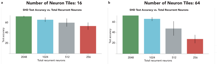
### Visual Description
\n
## Bar Charts: SHD Test Accuracy vs. Total Recurrent Neurons
### Overview
The image presents two bar charts (labeled 'a' and 'b') comparing SHD (Symmetric Hausdorff Distance) test accuracy against the total number of recurrent neurons. Each chart represents a different number of neuron tiles: 16 in chart 'a' and 64 in chart 'b'. The x-axis represents the total number of recurrent neurons, and the y-axis represents the test accuracy. Error bars are included on each bar.
### Components/Axes
* **Chart a:**
* Title: "Number of Neuron Tiles: 16"
* Subtitle: "SHD Test Accuracy vs. Total Recurrent Neurons"
* X-axis Label: "Total recurrent neurons"
* X-axis Markers: 2048, 1024, 512, 256
* Y-axis Label: "Test accuracy"
* **Chart b:**
* Title: "Number of Neuron Tiles: 64"
* Subtitle: "SHD Test Accuracy vs. Total Recurrent Neurons"
* X-axis Label: "Total recurrent neurons"
* X-axis Markers: 2048, 1024, 512, 256
* Y-axis Label: "Test accuracy"
* **Color Scheme:**
* 2048 neurons: Green
* 1024 neurons: Light Blue
* 512 neurons: Gray
* 256 neurons: Red
### Detailed Analysis or Content Details
**Chart a (16 Neuron Tiles):**
* **2048 Neurons:** The green bar indicates a test accuracy of approximately 68. The error bar extends from roughly 65 to 71.
* **1024 Neurons:** The light blue bar shows a test accuracy of approximately 64. The error bar extends from roughly 61 to 67.
* **512 Neurons:** The gray bar indicates a test accuracy of approximately 59. The error bar extends from roughly 56 to 62.
* **256 Neurons:** The red bar shows a test accuracy of approximately 52. The error bar extends from roughly 49 to 55.
**Chart b (64 Neuron Tiles):**
* **2048 Neurons:** The green bar indicates a test accuracy of approximately 68. The error bar extends from roughly 65 to 71.
* **1024 Neurons:** The light blue bar shows a test accuracy of approximately 64. The error bar extends from roughly 61 to 67.
* **512 Neurons:** The gray bar indicates a test accuracy of approximately 46. The error bar extends from roughly 43 to 49.
* **256 Neurons:** The red bar shows a test accuracy of approximately 30. The error bar extends from roughly 27 to 33.
### Key Observations
* In both charts, the test accuracy generally decreases as the number of recurrent neurons decreases.
* The highest accuracy is achieved with 2048 neurons in both scenarios.
* The difference in accuracy between 2048 and 1024 neurons is relatively small.
* The accuracy drop from 512 to 256 neurons is more substantial.
* Chart 'b' (64 neuron tiles) shows a more pronounced decrease in accuracy with fewer neurons compared to chart 'a' (16 neuron tiles).
### Interpretation
The data suggests that increasing the number of recurrent neurons generally improves SHD test accuracy, up to a point. However, the benefit of adding more neurons diminishes as the number increases. The difference in performance between 16 and 64 neuron tiles indicates that the configuration of neuron tiles impacts the effectiveness of increasing the number of recurrent neurons. With 64 tiles, the accuracy drops more significantly when reducing the number of neurons. This could indicate that a certain level of granularity (provided by the 16 tiles) is necessary to fully utilize a larger number of recurrent neurons. The error bars suggest that the observed differences in accuracy are statistically significant, but there is still some variability in the results. The charts demonstrate a trade-off between model complexity (number of neurons) and performance (test accuracy).
</details>
a
<details>
<summary>Image 57 Details</summary>
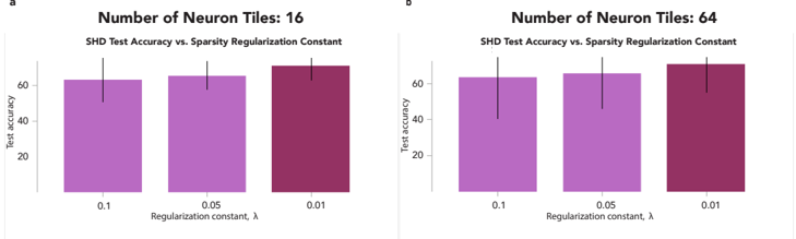
### Visual Description
\n
## Bar Charts: SHD Test Accuracy vs. Sparsity Regularization Constant
### Overview
The image presents two bar charts, labeled 'a' and 'b', comparing SHD (Structural Hamming Distance) Test Accuracy against the Sparsity Regularization Constant (λ) for different numbers of neuron tiles. Chart 'a' shows results for 16 neuron tiles, while chart 'b' shows results for 64 neuron tiles. Each chart displays three bars representing different regularization constants: 0.1, 0.05, and 0.01. Error bars are present on top of each bar, indicating the variability in the test accuracy.
### Components/Axes
* **X-axis:** "Regularization constant, λ" with markers at 0.1, 0.05, and 0.01.
* **Y-axis:** "Test accuracy" with a scale ranging from 20 to 70, incrementing by 10.
* **Titles:**
* Chart a: "Number of Neuron Tiles: 16" and "SHD Test Accuracy vs. Sparsity Regularization Constant"
* Chart b: "Number of Neuron Tiles: 64" and "SHD Test Accuracy vs. Sparsity Regularization Constant"
* **Bars:** Represent test accuracy for each regularization constant.
* **Error Bars:** Indicate the standard deviation or confidence interval of the test accuracy.
### Detailed Analysis or Content Details
**Chart a (16 Neuron Tiles):**
* **λ = 0.1:** The bar is approximately at a height of 64. The error bar extends from approximately 60 to 68.
* **λ = 0.05:** The bar is approximately at a height of 63. The error bar extends from approximately 59 to 67.
* **λ = 0.01:** The bar is approximately at a height of 66. The error bar extends from approximately 62 to 70.
**Chart b (64 Neuron Tiles):**
* **λ = 0.1:** The bar is approximately at a height of 61. The error bar extends from approximately 57 to 65.
* **λ = 0.05:** The bar is approximately at a height of 60. The error bar extends from approximately 56 to 64.
* **λ = 0.01:** The bar is approximately at a height of 65. The error bar extends from approximately 61 to 69.
In both charts, the bars are colored in shades of purple, with the bar corresponding to λ = 0.01 being the darkest shade.
### Key Observations
* In both charts, the test accuracy generally increases as the regularization constant (λ) increases from 0.1 to 0.01.
* The error bars suggest that the variability in test accuracy is similar across different regularization constants for both 16 and 64 neuron tiles.
* The difference in test accuracy between the different regularization constants is relatively small, especially for 16 neuron tiles.
* The test accuracy is slightly higher for 64 neuron tiles compared to 16 neuron tiles, particularly at λ = 0.01.
### Interpretation
The data suggests that increasing the sparsity regularization constant (λ) generally leads to a slight improvement in SHD test accuracy. This indicates that introducing more sparsity in the model can be beneficial for performance. The relatively small differences in test accuracy between the different regularization constants suggest that the model is not highly sensitive to the choice of λ within the tested range.
The slightly higher test accuracy observed for 64 neuron tiles compared to 16 neuron tiles suggests that increasing the number of neuron tiles can also improve performance, potentially by allowing the model to learn more complex representations. However, the improvement is not substantial, and the optimal number of neuron tiles may depend on other factors, such as the size and complexity of the dataset.
The error bars indicate that the results are subject to some variability, and further experiments with larger sample sizes may be needed to confirm these findings. The charts demonstrate a trade-off between model complexity (number of neuron tiles) and regularization strength (λ), and the optimal balance between these two factors may depend on the specific application and dataset.
</details>
b
F igure A. 19 : SHD keyword spotting dataset test accuracies for Mosaic architectures trained with different sparsity regularization values. As explained in the Methods section of the main text, the regularization is added to the loss function to exponentially penalize the long-range connections. The plot shows the accuracy for strong (default, λ = 0.1), medium ( λ = 0.05) and weaker ( λ = 0.01) sparsity regularization on a) 4 x 4 neuron tile layout and b) 8 x 8 neuron tile layout. Median and standard deviation are calculated using 4 experiments with varying number of neurons per neuron tile.
## supplementary note 8
<details>
<summary>Image 58 Details</summary>
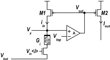
### Visual Description
\n
## Diagram: Operational Amplifier Circuit
### Overview
The image depicts a schematic diagram of an operational amplifier (op-amp) circuit, likely a current mirror configuration with feedback. The circuit consists of two MOSFETs (M1 and M2), an op-amp (labeled 'A'), and a third MOSFET (labeled with 'Gᵢ'). The diagram illustrates the connections and flow of signals within the circuit.
### Components/Axes
The diagram contains the following labeled components:
* **M1:** MOSFET, positioned at the top-left.
* **M2:** MOSFET, positioned at the top-right.
* **A:** Operational Amplifier, positioned in the center-right. The '+' and '-' signs indicate the non-inverting and inverting inputs, respectively.
* **Gᵢ:** MOSFET, positioned in the center-bottom.
* **V<sub>out</sub>:** Output voltage, positioned at the top-center.
* **V<sub>in</sub>:** Input voltage, positioned at the bottom-center.
* **V<sub>top</sub>:** Voltage at the top node, positioned to the right of Gᵢ.
* **V<sub>bot</sub>:** Voltage at the bottom node, positioned below Gᵢ.
* **i<sub>in</sub>:** Input current, positioned to the left of Gᵢ.
* **I<sub>out</sub>:** Output current, positioned below M2.
There are no axes in this diagram. It is a schematic representation, not a graph.
### Detailed Analysis / Content Details
The circuit operates as follows:
1. **Input:** The input voltage (V<sub>in</sub>) is applied to the gate of MOSFET Gᵢ.
2. **Current Flow:** The input current (i<sub>in</sub>) flows through MOSFET Gᵢ.
3. **Op-Amp Feedback:** The output voltage (V<sub>out</sub>) of the op-amp is connected to the gate of MOSFET M1. The op-amp attempts to maintain the voltage at the inverting input equal to the voltage at the non-inverting input.
4. **Current Mirroring:** MOSFETs M1 and M2 form a current mirror. The current flowing through M1 is mirrored by M2, resulting in an output current (I<sub>out</sub>).
5. **Voltage Regulation:** The op-amp provides feedback to regulate the output voltage (V<sub>out</sub>) and ensure that the current through M2 is proportional to the input current (i<sub>in</sub>).
The diagram does not provide specific numerical values for component parameters (e.g., resistance, capacitance, transistor characteristics). It is a conceptual representation of the circuit.
### Key Observations
* The circuit is designed to create a current mirror with feedback control.
* The op-amp is used to improve the accuracy and stability of the current mirror.
* The MOSFET Gᵢ acts as a current source controlled by the input voltage V<sub>in</sub>.
* The circuit is likely intended to provide a stable and predictable output current (I<sub>out</sub>) based on the input voltage (V<sub>in</sub>).
### Interpretation
This circuit is a classic example of a current mirror with an op-amp used for feedback and improved performance. The op-amp forces the voltage at the drain of M1 to be equal to V<sub>in</sub>, which in turn controls the current through M2. This configuration is commonly used in analog integrated circuit design for applications such as bias current generation, current sources, and active loads. The absence of specific component values suggests that the diagram is intended to illustrate the fundamental principle of operation rather than a specific implementation. The circuit's effectiveness relies on the matching characteristics of the MOSFETs and the performance of the op-amp. The feedback loop created by the op-amp ensures that the output current is relatively insensitive to variations in the op-amp's gain or the MOSFETs' threshold voltages.
</details>
bot
F igure A. 20 : Analysis of the read-out circuitry. The amplifier with gain A, pins voltage Vx to the voltage Vtop . On the arrival of the pulse on Vin < i > , a current equal to i in = ( Vtop -Vbot ) Gi flows into the memristor i , which is then mirrored out iout .
supplementary note 9 Figure A. 20 details the implementation of the read-out circuit used in the Mosaic architecture. Though not optimized for area, we have used this implementation for both the neuron and routing tiles.
The dominant power consumption of the circuit depends on the required bandwidth (BW) of the feedback loop. This BW depends on the maximum conductance of the RRAM, Gmax . For Gi , max , once an input arrives to Vin < i > , the current i in has to settle to ( Vtop -Vbot ) Gi , max within a settling time, ts , a proportion of the pulse width. This timing sets the speed at which the loop should work, and thus its BW. If the loop does not close in this time, the amplifier will slew, and the voltage Vx drops. In both neuron and routing tiles, this condition should be met for Vx to stay pinned at Vtop while RRAM is being read. However, the neuron and routing tiles have different BW requirements.
In the neuron tile , the read-out circuitry has to resolve between at least 8 levels of current for the 8 levels that each RRAM device can take. Therefore, the Least Significant Bit (LSB) of the i in current for the neuron tile is i in , LSB , N = Vref ( Gmax -Gmin ) N . Based on the Fig. 5 . 2 d, this value for the neuron tile is 100 mV ( 120 µ S -40 µ S ) 8 = 1 µ A . Note that since the 8 levels to be resolved are in the Low Resistive State of the RRAM, the Gmax and Gmin are the minimum and maximum of the range in the LRS, which correspond to 40 µ S and 120 µ S .
In the routing tile , the read-out circuitry has to resolve between two levels which will either let the spike regenerate and thus propagate, or will get blocked. Therefore, the LSB of the i in current in the routing tile is i in , LSB , R = Vref ( Gmax -Gmin ) N . Based on the Fig. 5 . 2 d, this value for the neuron
tile is 100 mV ( 40 µ S -10 µ S ) 2 = 15 µ A . Note that since the 2 levels to be resolved are the LRS and HRS of the RRAM, the Gmax and Gmin correspond to 10 µ S and 40 µ S .
To be able to distinguish between any two levels in both cases, we will consider a maximum error of i in , LSB 2 . Therefore, the maximum tolerable error in the the neuron tile is 0.5 µ A and in the routing tile is 7.5 µ A .
This means that if the feedback loop does not close in ts of the pulse width, Vx drop is a lot more tolerable in the routing tile than it is in the neuron tile. This suggests that the bandwidth requirements in the case of neuron tile is 7.5/0.5 = 15 times more than that of the routing tile. The BW requirements directly translate to the biasing of the amplifier and thus its power consumption. Therefore, the static power consumption of the neuron tile is 15 times that of the routing tile. The current requirements also translate to area, since larger currents require wider transistors.
appendix 3 : reconfigurable halide perovskite nanocrystal memristors for neuromorphic computing
F igure A. 21 : Proposed volatile diffusive switching mechanism. (a-d) illustrate the various stages of filament formation and rupture. i-iv indicate the possible reactions happening within the device.
<details>
<summary>Image 59 Details</summary>
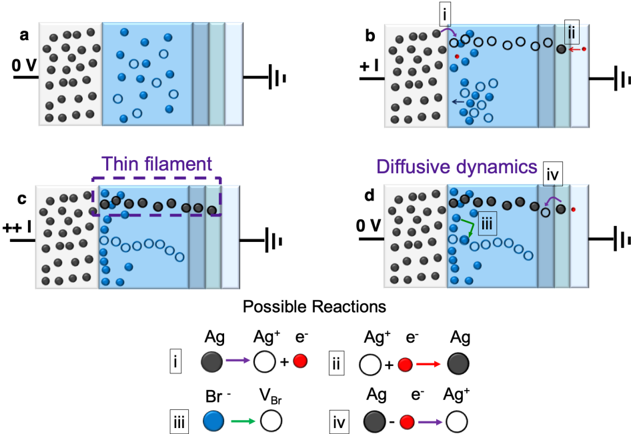
### Visual Description
\n
## Diagram: Ionic Transport and Filament Formation
### Overview
The image presents a schematic diagram illustrating ionic transport and the formation of a thin filament across a membrane-like structure, likely representing an electrochemical cell. Four panels (a-d) depict different stages or conditions, with associated reaction schemes below. The diagram uses visual cues like particle distribution and arrows to represent ion movement and chemical reactions.
### Components/Axes
The diagram consists of four panels labeled a, b, c, and d, arranged in a 2x2 grid. Each panel shows a partitioned space with a membrane-like structure separating two regions. Each region has a battery symbol indicating a potential difference. The panels also contain black and blue circles representing ions, and arrows indicating their movement. Below the panels is a section labeled "Possible Reactions" with four numbered reactions (i-iv) depicting chemical processes.
### Detailed Analysis or Content Details
**Panel a:**
* Voltage: 0V.
* Left side: High concentration of black circles (likely representing Ag+ ions).
* Right side: Scattered blue circles (likely representing Br- ions) and some empty circles.
* No apparent directed movement of ions.
**Panel b:**
* Voltage: +1.
* Left side: High concentration of black circles.
* Right side: Fewer black circles, more empty circles, and blue circles.
* Arrows:
* i: Black circle moving from left to right, labeled "Ag -> Ag+ + e-".
* ii: Empty circle moving from right to left, labeled "Ag+ + e- -> Ag".
* Arrows indicate ion transport across the membrane.
**Panel c:**
* Voltage: ++.
* Left side: High concentration of black circles.
* Right side: A purple line (representing a "Thin filament") is formed, connecting the two sides.
* Arrows:
* Purple line indicates the formation of a conductive path.
**Panel d:**
* Voltage: 0V.
* Left side: High concentration of black circles.
* Right side: Scattered blue circles and empty circles.
* Arrows:
* iii: Blue circle moving from right to left, labeled "Br -> VBr".
* iv: Black circle moving from left to right, labeled "Ag + e- -> Ag+".
**Possible Reactions:**
* i: Ag -> Ag+ + e- (Silver oxidation)
* ii: Ag+ + e- -> Ag (Silver reduction)
* iii: Br -> VBr (Bromine vacancy formation)
* iv: Ag + e- -> Ag+ (Silver oxidation)
### Key Observations
* The diagram illustrates the formation of a conductive filament (Panel c) under an applied voltage (Panel b).
* The reactions suggest a redox process involving silver ions (Ag and Ag+) and electron transfer.
* The presence of bromine (Br) and its vacancy (VBr) suggests an ionic conduction mechanism.
* The voltage changes influence the ion distribution and reaction pathways.
### Interpretation
The diagram depicts a process of ion migration and filament formation, likely related to resistive switching or memristive behavior in a solid electrolyte. The applied voltage drives the movement of silver ions (Ag+) and bromine ions (Br-), leading to the formation of a conductive filament composed of silver. The reactions show the oxidation and reduction of silver, coupled with the creation of bromine vacancies to facilitate ion transport. The diagram suggests that the filament formation is driven by electrochemical reactions and ion diffusion. The change in voltage from 0V to +1V and ++V is critical for initiating and sustaining the filament growth. The final state (Panel d) shows a return to a more dispersed state, potentially indicating a reset or switching process. The diagram is a simplified representation of a complex electrochemical process, but it effectively conveys the key mechanisms involved in filament formation and resistive switching.
</details>
supplementary note 1 Diffusive behaviour: The volatile threshold switching behaviour can be attributed to the redistribution of Ag + and Br -ions under an applied electric field, and their back-diffusion upon removing power. The soft lattice of the halide perovskite matrix has been observed to enable Ag + migration with an activation energy ∼ 0.15eV 2 . Interestingly, migration of halide ions and their vacancies within the perovskite matrix also occur at similar energies ∼ 0.10 -0.25eV [ 253 , 348 , 349 ], making it difficult to pinpoint a singular operation mechanism. We hypothesize that during the SET process, Ag atoms are ionized to Ag + and forms a percolation path through the device structure. Electrons from the grounded electrode oxidize Ag + to form weak Ag filaments. Parallelly, Br -ions get attracted towards the positively charged electrode and a weak filament composed of vacancies ( VBr ) is formed. Both these factors increase the device conductance from a high resistance state (HRS) to a temporary low resistance state (LRS). Upon removing the electric field, the low activation energy of the ions causes them to diffuse back spontaneously, breaking the percolation path and leading to volatile memory characteristics a.k.a. short-term plasticity. The low compliance current ( Icc ) of 1 µ A ensures that the electrochemical reactions are well regulated, and the percolation pathways formed are weak enough to allow these diffusive dynamics.
F igure A. 22 : Proposed non-volatile drift switching mechanism. (a-e) illustrate the various stages of filament formation and rupture. i-iv indicate the possible reactions happening within the device.
<details>
<summary>Image 60 Details</summary>
### Visual Description
\n
## Diagram: Electrochemical Filament Formation and Dynamics
### Overview
The image presents a schematic diagram illustrating the formation and dynamics of a silver (Ag) filament within an electrolyte, likely a solid-state electrolyte, under varying applied voltages. The diagram consists of five panels (a-e) depicting different stages of the process, along with a "Possible Reactions" key explaining the chemical processes involved. The panels show the distribution of silver ions (Ag⁺, represented by grey circles), silver atoms (Ag, represented by black circles), bromide ions (Br⁻, represented by blue circles), and electrons (e⁻). Each panel also includes a schematic representation of electrodes with applied voltage indicated.
### Components/Axes
The diagram does not have traditional axes. Instead, it uses visual representations of components within a cell:
* **Electrode:** Represented by vertical lines on the right and left sides of each panel.
* **Electrolyte:** The blue shaded region between the electrodes.
* **Silver Ions (Ag⁺):** Grey circles.
* **Silver Atoms (Ag):** Black circles.
* **Bromide Ions (Br⁻):** Blue circles.
* **Electrons (e⁻):** Not explicitly shown as circles, but indicated in the "Possible Reactions" key.
* **Voltage:** Indicated numerically next to the electrodes (0V, +1, +++, -V).
* **Arrows:** Indicate movement or reaction direction.
* **Labels:** i, ii, iii, iv are used to label specific reactions in the "Possible Reactions" key.
### Detailed Analysis or Content Details
**Panel a (0V):**
* Silver ions (grey) and bromide ions (blue) are distributed randomly within the electrolyte.
* No applied voltage is indicated.
**Panel b (+1):**
* A positive voltage (+1) is applied.
* Silver ions (grey) are migrating towards the left electrode.
* Some silver ions are reduced to silver atoms (black) near the left electrode, indicated by reaction 'i' with a purple arc.
* Reaction 'i' is described as Ag⁺ + e⁻ → Ag.
* Reaction 'ii' is described as Ag⁺ + e⁻ → Ag.
* Arrows indicate the movement of ions and electrons.
**Panel c (+++):**
* A high positive voltage (+++) is applied.
* A "thick filament" of silver atoms (black) has formed, connecting the two electrodes.
* Silver ions continue to migrate towards the left electrode.
* The dashed line indicates the extent of the filament.
**Panel d (0V):**
* Voltage is returned to 0V.
* The filament remains, but silver ions (grey) are shown drifting within the electrolyte, indicated by "Drift dynamics".
* The blue circles (Br⁻) are also shown drifting.
**Panel e (-V):**
* A negative voltage (-V) is applied.
* Silver atoms (black) are dissolving from the right electrode.
* Reaction 'iii' is described as Br⁻ → VBr.
* Reaction 'iv' is described as Ag → Ag⁺ + e⁻.
* Arrows indicate the dissolution of silver and the movement of ions.
**Possible Reactions Key:**
* **i:** Ag⁺ + e⁻ → Ag
* **ii:** Ag⁺ + e⁻ → Ag
* **iii:** Br⁻ → VBr
* **iv:** Ag → Ag⁺ + e⁻
### Key Observations
* The formation of the silver filament is driven by a positive voltage, causing silver ions to reduce to silver atoms.
* The filament persists even when the voltage is removed.
* A negative voltage causes the filament to dissolve, reversing the reaction.
* The reactions involve the transfer of electrons and the movement of ions.
* The "VBr" in reaction iii is unclear, potentially representing a vacancy or a complex.
### Interpretation
This diagram illustrates the mechanism of resistive switching in a solid-state electrolyte. The formation of a conductive silver filament under a positive voltage explains the low-resistance state, while its dissolution under a negative voltage explains the high-resistance state. This is a common principle behind resistive random-access memory (RRAM) devices. The reactions shown are simplified representations of the electrochemical processes occurring at the electrodes and within the electrolyte. The drift dynamics in panel d suggest that the filament is not perfectly stable and may undergo some structural changes even at zero voltage. The unclear "VBr" in reaction iii suggests a more complex electrochemical process involving bromide ions, potentially related to the creation of defects or vacancies within the electrolyte to facilitate ion transport. The diagram provides a conceptual understanding of the filament formation and switching mechanism, but further details about the electrolyte composition and device structure would be needed for a more complete analysis.
</details>
supplementary note 2 Drift behaviour: Upon increasing the Icc to 1 mA ( 3 orders of magnitude higher than that used for volatile threshold switching), permanent and thicker conductive filamentary pathways are possibly formed within the device as illustrated in Fig. A. 22 . This increases the device conductance from a high resistance state (HRS) to a permanent and much lower low resistance state (LRS). Electrochemical reactions are triggered to a higher extent and hence, the switching dynamics is now dominated by the drift kinetics of the mobile ion species Ag + and Br -, rather than diffusion. Hence upon removing the electric field, the conductive filaments remain largely unaffected, and the devices retain their LRS and portray longterm plasticity. Application of voltage sweeps, or pulses of opposite polarity causes rupture of these filaments, and the devices are reset to their HRS. For DDAB-capped CsPbBr3NCs, the devices transition to a non-erasable non-volatile state within ∼ 50 cycles, indicating formation of very thick filaments (Fig. A. 23 ) On the other hand, the OGB-capped CsPbBr3 NCs display a record-high nonvolatile endurance of 5655 cycles and retention of 10 5 seconds (Fig. A. 24 ), pointing to better regulation of the filament formation and rupture kinetics.
F igure A. 23 : Non-volatile drift switching of DDAB-capped CsPbBr 3 NC memristors. (a) Representative IV characteristics. (b) Endurance. (c) Retention.
<details>
<summary>Image 61 Details</summary>
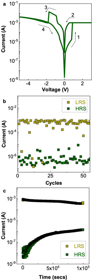
### Visual Description
## Chart: I-V and Retention Characteristics
### Overview
The image presents three charts related to the electrical characteristics of a device, likely a memristor or similar resistive switching element. Chart (a) shows a current-voltage (I-V) hysteresis loop. Chart (b) displays the current as a function of cycling number, demonstrating retention behavior. Chart (c) shows the current as a function of time, also related to retention. All charts use a logarithmic scale for the current axis.
### Components/Axes
* **Chart (a):**
* X-axis: Voltage (V), ranging from approximately -5V to 2V.
* Y-axis: Current (A), logarithmic scale from 10^-9 A to 10^-1 A.
* Curves labeled 1, 2, 3, and 4 represent different sweeps of the I-V curve.
* **Chart (b):**
* X-axis: Cycles, ranging from 0 to approximately 55.
* Y-axis: Current (A), logarithmic scale from 10^-9 A to 10^-2 A.
* Data points are represented by two distinct markers: Yellow squares (LRS - Low Resistance State) and Green squares (HRS - High Resistance State).
* Legend is located in the top-right corner.
* **Chart (c):**
* X-axis: Time (secs), ranging from 0 to approximately 1x10^5 seconds.
* Y-axis: Current (A), logarithmic scale from 10^-9 A to 10^-3 A.
* Data points are represented by two distinct markers: Yellow squares (LRS - Low Resistance State) and Green squares (HRS - High Resistance State).
* Legend is located in the bottom-right corner.
### Detailed Analysis or Content Details
* **Chart (a):**
* Curve 1: Starts at approximately 10^-5 A at -5V, increases to approximately 10^-3 A at -2V, then drops sharply to approximately 10^-7 A at 0V, and then increases to approximately 10^-3 A at 2V.
* Curve 2: Starts at approximately 10^-3 A at 2V, decreases to approximately 10^-5 A at 0V, then drops sharply to approximately 10^-7 A at -2V, and then increases to approximately 10^-3 A at -4V.
* Curve 3: Starts at approximately 10^-1 A at -4V, decreases to approximately 10^-3 A at -2V, then drops sharply to approximately 10^-7 A at 0V, and then increases to approximately 10^-3 A at 2V.
* Curve 4: Starts at approximately 10^-3 A at 0V, decreases to approximately 10^-7 A at -2V, and then increases to approximately 10^-3 A at -4V.
* The hysteresis loop indicates a non-linear resistive switching behavior.
* **Chart (b):**
* LRS (Yellow): The current remains relatively stable at approximately 10^-4 A throughout the 55 cycles, with some minor fluctuations.
* HRS (Green): The current remains relatively stable at approximately 10^-6 A throughout the 55 cycles, with some minor fluctuations.
* The difference between the LRS and HRS currents demonstrates the retention capability of the device.
* **Chart (c):**
* LRS (Yellow): The current starts at approximately 10^-5 A and increases to approximately 10^-3 A over the 1x10^5 seconds.
* HRS (Green): The current starts at approximately 10^-7 A and increases to approximately 10^-5 A over the 1x10^5 seconds.
* The gradual increase in current for both states indicates a drift in resistance over time.
### Key Observations
* Chart (a) shows a clear hysteresis loop, indicating a resistive switching characteristic.
* Chart (b) demonstrates good retention of the LRS and HRS over 55 cycles. The separation between the two states is significant.
* Chart (c) shows a slight drift in the current for both LRS and HRS over time, suggesting some degradation in retention.
### Interpretation
The data suggests the device exhibits resistive switching behavior, capable of transitioning between a low resistance state (LRS) and a high resistance state (HRS). The I-V curve (Chart a) confirms this, with the hysteresis loop demonstrating the non-volatile nature of the switching. The retention characteristics (Charts b and c) show that the device can maintain these states for a considerable number of cycles and time, although some drift is observed over longer durations. The observed drift in Chart (c) could be due to various factors, such as material degradation or environmental effects. The consistent separation between LRS and HRS in Chart (b) is a positive indicator of the device's reliability. These characteristics are typical of memristive devices, which are promising candidates for non-volatile memory applications.
</details>
F igure A. 24 : Non-volatile drift switching of OGB-capped CsPbBr 3 NC memristors. Figure shows the retention performance.
<details>
<summary>Image 62 Details</summary>
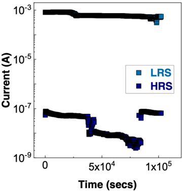
### Visual Description
\n
## Chart: Current vs. Time for LRS and HRS
### Overview
The image presents a chart displaying the relationship between Current (in Amperes) and Time (in seconds) for two states: Low Resistance State (LRS) and High Resistance State (HRS). The data is presented as a series of connected points, suggesting a time-dependent measurement. There are two distinct curves, one representing LRS and the other HRS.
### Components/Axes
* **X-axis:** Time (secs), ranging from approximately 0 to 1 x 10<sup>5</sup> seconds. The scale is logarithmic.
* **Y-axis:** Current (A), ranging from 10<sup>-9</sup> to 10<sup>-3</sup> Amperes. The scale is logarithmic.
* **Legend:** Located in the top-right corner.
* LRS (Light Blue squares)
* HRS (Dark Blue squares)
### Detailed Analysis
**HRS (Dark Blue Squares):**
The HRS curve begins at approximately 7 x 10<sup>-8</sup> A at time 0. It remains relatively stable until approximately 5 x 10<sup>4</sup> seconds, where it begins to decrease. The current drops rapidly to approximately 2 x 10<sup>-9</sup> A at around 7.5 x 10<sup>4</sup> seconds. After this drop, the current increases again to approximately 1 x 10<sup>-7</sup> A at 1 x 10<sup>5</sup> seconds.
**LRS (Light Blue Squares):**
The LRS curve starts at approximately 2 x 10<sup>-3</sup> A at time 0. It exhibits a slight downward trend, decreasing to approximately 1 x 10<sup>-3</sup> A by 5 x 10<sup>4</sup> seconds. The current then increases slightly to approximately 1.5 x 10<sup>-3</sup> A at 1 x 10<sup>5</sup> seconds.
### Key Observations
* The HRS exhibits a significant drop in current around 7.5 x 10<sup>4</sup> seconds, followed by a slight recovery.
* The LRS maintains a significantly higher current level throughout the measured time period compared to the HRS.
* Both curves show some degree of fluctuation, but the HRS curve demonstrates a more pronounced change in current.
* The logarithmic scales on both axes compress the data, making it difficult to discern precise values without closer inspection.
### Interpretation
The chart likely represents the behavior of a resistive switching memory device (e.g., memristor). The LRS and HRS correspond to the two distinct resistance states of the device. The observed switching behavior – the drop in current for HRS – suggests a transition between these states. The data indicates that the device can be switched from a high resistance state to a low resistance state and back again, demonstrating its non-volatile memory capability. The fluctuations in current could be due to noise, measurement errors, or inherent device variability. The time scale suggests that the switching process occurs on the order of tens of thousands of seconds. The large difference in current between LRS and HRS indicates a substantial difference in resistance, which is crucial for reliable memory operation. The initial stability of the HRS before the drop suggests a holding time or a threshold for switching.
</details>
F igure A. 25 : Transmission electron microscope (TEM) images of DDAB-capped CsPbBr 3 NCs.
<details>
<summary>Image 63 Details</summary>
### Visual Description
\n
## Micrograph: Nanostructured Material
### Overview
The image is a grayscale micrograph depicting a highly ordered, two-dimensional nanostructure. The structure consists of a repeating pattern of interconnected square or rectangular cells, resembling a lattice or mesh. The image appears to be a transmission electron microscopy (TEM) image, given the high contrast and resolution.
### Components/Axes
The only explicit label present is a scale bar located in the bottom-left corner, indicating a length of "10 nm". There are no axes or legends present. The image itself represents the sample being observed.
### Detailed Analysis or Content Details
The nanostructure is composed of dark lines forming the walls of the cells, and lighter areas within the cells. The cells are approximately square, with an estimated side length of 2-3 nm. The lines appear to have a consistent width throughout the image. The structure is highly uniform, with minimal defects or irregularities visible. The overall image is approximately 500x500 pixels. The contrast between the cell walls and the interior is high, suggesting a difference in material composition or density.
### Key Observations
The most striking observation is the high degree of order and uniformity in the nanostructure. The repeating pattern suggests a self-assembly process or a highly controlled fabrication method. The scale bar indicates that the features are in the nanometer range, confirming the nanoscale nature of the structure. There are no obvious variations in cell size or shape across the image.
### Interpretation
The image likely represents a synthesized material with a designed nanostructure. The regular arrangement of cells suggests potential applications in areas such as catalysis, energy storage, or filtration, where a high surface area and controlled pore size are desirable. The material could be a metal-organic framework (MOF), a zeolite, or another type of porous material. The high contrast suggests that the cell walls are composed of a material with a significantly different electron scattering cross-section than the material within the cells. Further analysis, such as energy-dispersive X-ray spectroscopy (EDS), would be needed to determine the elemental composition of the material and confirm its structure. The image provides strong evidence for the successful fabrication of a well-defined nanostructure. The lack of defects suggests a high degree of control over the synthesis process.
</details>
supplementary note 3
F igure A. 26 : Non-linear variation of the device conductance as a function of the stimulation pulse (a) amplitude, (b) width and (c) number. For (a), the pulse width and number is kept constant at 25 ms and 1 respectively. For (b), the pulse amplitude and number is kept constant at 1 V and 1 respectively. For (c), the pulse amplitude and width is kept constant at 1 V and 25 ms respectively.
<details>
<summary>Image 64 Details</summary>
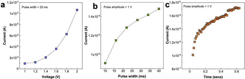
### Visual Description
## Charts: Current vs. Voltage, Pulse Width, and Time
### Overview
The image presents three separate charts (a, b, and c) illustrating the relationship between current and other parameters. Chart (a) shows current as a function of voltage, (b) shows current as a function of pulse width, and (c) shows current as a function of time. All charts appear to represent experimental data.
### Components/Axes
* **Chart a:**
* X-axis: Voltage (V), ranging from approximately 1.15V to 2.0V.
* Y-axis: Current (A), ranging from 0A to 1.2 x 10^-5 A.
* Title: "Pulse width = 25 ms"
* Data Series: Single series represented by blue squares.
* **Chart b:**
* X-axis: Pulse width (ms), ranging from approximately 10ms to 40ms.
* Y-axis: Current (A), ranging from approximately 2 x 10^-6 A to 1.5 x 10^-5 A.
* Title: "Pulse amplitude = 1 V"
* Data Series: Single series represented by green squares.
* **Chart c:**
* X-axis: Time (secs), ranging from approximately 0.05s to 0.6s.
* Y-axis: Current (A), ranging from approximately 8 x 10^-7 A to 1.8 x 10^-5 A.
* Title: "Pulse amplitude = 1 V"
* Data Series: Single series represented by orange squares.
### Detailed Analysis or Content Details
* **Chart a:** The blue data series shows a strong positive correlation between voltage and current. The line slopes sharply upwards.
* (1.15V, 1.0 x 10^-6 A)
* (1.25V, 1.8 x 10^-6 A)
* (1.35V, 2.6 x 10^-6 A)
* (1.45V, 3.5 x 10^-6 A)
* (1.6V, 4.8 x 10^-6 A)
* (1.8V, 6.2 x 10^-6 A)
* (2.0V, 1.15 x 10^-5 A)
* **Chart b:** The green data series shows a positive correlation between pulse width and current. The line slopes upwards, but the increase in current appears to slow down at higher pulse widths.
* (10ms, 2.0 x 10^-6 A)
* (15ms, 4.0 x 10^-6 A)
* (20ms, 6.0 x 10^-6 A)
* (25ms, 8.0 x 10^-6 A)
* (30ms, 1.0 x 10^-5 A)
* (35ms, 1.2 x 10^-5 A)
* (40ms, 1.5 x 10^-5 A)
* **Chart c:** The orange data series shows a positive correlation between time and current. The line slopes upwards, but the increase in current appears to slow down at higher times.
* (0.05s, 8.0 x 10^-7 A)
* (0.1s, 1.5 x 10^-6 A)
* (0.2s, 4.0 x 10^-6 A)
* (0.3s, 8.0 x 10^-6 A)
* (0.4s, 1.2 x 10^-5 A)
* (0.5s, 1.5 x 10^-5 A)
* (0.6s, 1.75 x 10^-5 A)
### Key Observations
* All three charts demonstrate a positive relationship between the independent variable and current.
* The relationship between voltage and current (Chart a) appears to be the most linear.
* The relationships between pulse width/time and current (Charts b and c) show diminishing returns, suggesting a saturation effect.
### Interpretation
The data suggests that current increases with increasing voltage, pulse width, and time. The saturation observed in Charts b and c could indicate a limit to the current that can be induced by increasing pulse width or time, potentially due to the material's properties or the experimental setup. Chart a demonstrates a linear relationship, which is consistent with Ohm's Law (V = IR), suggesting a constant resistance within the measured voltage range. The different pulse amplitudes and widths used in the experiments (indicated in the chart titles) likely influence the current flow, and the data provides insights into how these parameters affect the system's response. The data could be used to characterize the electrical behavior of a material or device under pulsed conditions.
</details>
F igure A. 27 : Echo state Properties. Variation in the device conductance of the volatile diffusive perovskite memristor as a function of the inter-group pulse interval. The interval between the two sequences increases from (a) 10 ms, (b) 30 ms to (c) 300 ms. (d-g) Current responses when subjected to 10 identical stimulation pulses ( 1 V, 5 ms ) with different pulse interval conditions for the final pulse. The interval varies from (d) 10 ms, (e) 23 ms, (f) 41 ms, to (g) 80 ms.
<details>
<summary>Image 65 Details</summary>
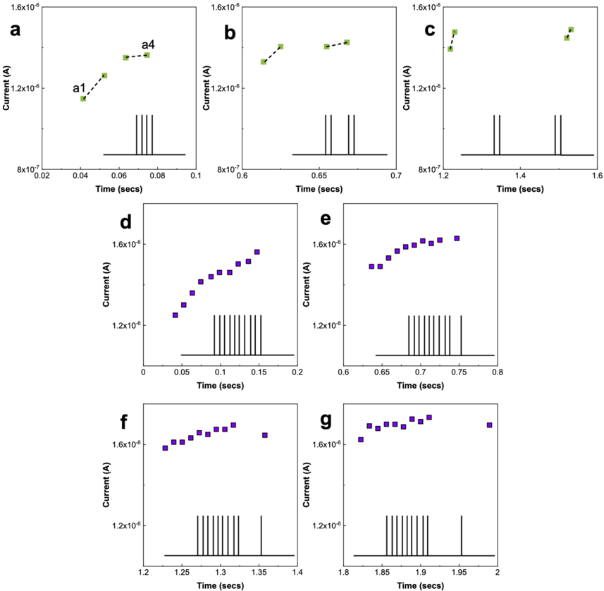
### Visual Description
## Charts: Current vs. Time Plots
### Overview
The image presents seven separate charts (labeled a through g) displaying current (in Amperes, A) as a function of time (in seconds, secs). Each chart shows a series of data points, some connected by lines, and a series of vertical lines at the bottom of each plot, likely representing a pulsed signal or measurement intervals. The y-axis scale is logarithmic.
### Components/Axes
* **X-axis (all charts):** Time (secs). Scales vary per chart.
* **Y-axis (all charts):** Current (A). Logarithmic scale, ranging approximately from 8x10<sup>-7</sup> A to 1.6x10<sup>-6</sup> A.
* **Chart a:** Green data points connected by a dashed line.
* **Chart b:** Green data points connected by a dashed line.
* **Chart c:** Green data points connected by a dashed line.
* **Chart d:** Purple data points.
* **Chart e:** Purple data points.
* **Chart f:** Purple data points.
* **Chart g:** Purple data points.
* **Bottom of each chart:** Series of vertical lines, indicating time intervals.
### Detailed Analysis or Content Details
**Chart a:**
* Trend: The line slopes upward, then plateaus.
* Data Points (approximate):
* (0.02 secs, 8.5x10<sup>-7</sup> A) - labeled "a1"
* (0.08 secs, 1.5x10<sup>-6</sup> A) - labeled "a4"
**Chart b:**
* Trend: The line initially rises, then fluctuates around a plateau.
* Data Points (approximate):
* (0.6 secs, 1.2x10<sup>-6</sup> A)
* (0.65 secs, 1.6x10<sup>-6</sup> A)
* (0.7 secs, 1.3x10<sup>-6</sup> A)
**Chart c:**
* Trend: The line rises, then fluctuates around a plateau.
* Data Points (approximate):
* (1.2 secs, 1.2x10<sup>-6</sup> A)
* (1.4 secs, 1.6x10<sup>-6</sup> A)
* (1.6 secs, 1.3x10<sup>-6</sup> A)
**Chart d:**
* Trend: The data points decrease in value as time increases.
* Data Points (approximate):
* (0 secs, 1.6x10<sup>-6</sup> A)
* (0.05 secs, 1.4x10<sup>-6</sup> A)
* (0.1 secs, 1.3x10<sup>-6</sup> A)
* (0.15 secs, 1.25x10<sup>-6</sup> A)
* (0.2 secs, 1.2x10<sup>-6</sup> A)
**Chart e:**
* Trend: The data points decrease in value as time increases.
* Data Points (approximate):
* (0.6 secs, 1.6x10<sup>-6</sup> A)
* (0.65 secs, 1.5x10<sup>-6</sup> A)
* (0.7 secs, 1.4x10<sup>-6</sup> A)
* (0.75 secs, 1.3x10<sup>-6</sup> A)
* (0.8 secs, 1.2x10<sup>-6</sup> A)
**Chart f:**
* Trend: The data points decrease in value as time increases.
* Data Points (approximate):
* (1.2 secs, 1.6x10<sup>-6</sup> A)
* (1.25 secs, 1.5x10<sup>-6</sup> A)
* (1.3 secs, 1.4x10<sup>-6</sup> A)
* (1.35 secs, 1.3x10<sup>-6</sup> A)
* (1.4 secs, 1.2x10<sup>-6</sup> A)
**Chart g:**
* Trend: The data points decrease in value as time increases.
* Data Points (approximate):
* (1.8 secs, 1.6x10<sup>-6</sup> A)
* (1.85 secs, 1.5x10<sup>-6</sup> A)
* (1.9 secs, 1.4x10<sup>-6</sup> A)
* (1.95 secs, 1.3x10<sup>-6</sup> A)
* (2 secs, 1.2x10<sup>-6</sup> A)
### Key Observations
* Charts a, b, and c show an initial rise in current followed by a plateau or fluctuation. These charts use green data points and dashed lines.
* Charts d, e, f, and g show a consistent decrease in current over time. These charts use purple data points.
* The vertical lines at the bottom of each chart suggest a periodic or pulsed measurement.
* The logarithmic y-axis emphasizes relative changes in current rather than absolute values.
### Interpretation
The data suggests two distinct behaviors: a rapid current increase followed by stabilization (charts a-c), and a current decay (charts d-g). The pulsed nature of the measurements (indicated by the vertical lines) implies that these measurements are taken during or after a stimulus. The green charts (a-c) might represent the current response *during* a pulse, while the purple charts (d-g) might represent the current decay *after* the pulse. The consistent decay in the purple charts suggests an exponential decay process. The initial rise in the green charts could be due to a charging or activation process. The different time scales of the charts suggest that the experiments were conducted with varying pulse durations or measurement intervals. The labels "a1" and "a4" suggest these are specific points of interest within chart a, potentially marking key stages in the current rise.
</details>
supplementary note 4 The echo state property of a reservoir refers to the impact that previous inputs have on the current reservoir state, and how that influence fades out with time. To test this, four short pulses of 1 V, 5 ms are applied to the device in a paired-pulse format and the device states are recorded. A non-linear accumulative behaviour is observed as a function of the paired-pulse interval. In Fig A. 27 a, a short paired-pulse interval of 10 ms results in an echo index (defined as ( a 4 a 1 ) ∗ 100 ) of 118%. Longer intervals ( 30 ms and 300 ms in Fig. A. 27 b,c) result in smaller echo indices ( 107.5% and 107.2% respectively), reflective of the short-term memory in the perovskite memristors. To further test the echo state property, three pulse trains consisting of 10 identical stimulation pulses ( 1 V, 5 ms ) are applied to the device and the device states are recorded. In all cases, a non-linear accumulative behaviour is observed. As shown in Fig. A. 27 d-g, short intervals ( ≤ 23 ms ) for the last stimulation pulse result in further accumulation while long intervals result in depression of the device state. This indicates that the present device state remembers the input temporal features in the recent past but not the far past, allowing the diffusive perovskite memristors to act as efficient reservoir elements.
F igure A. 28 : Input waveforms. A representative "Write" (amplitude = 1 V, pulse width = 20 ms ) and "Read" (amplitude = -0.5 V, pulse width = 5 ms ) spike train applied to the volatile perovskite memristors in the reservoir layer.
<details>
<summary>Image 66 Details</summary>
### Visual Description
\n
## Chart: Voltage vs. Time
### Overview
The image presents a time-domain plot of voltage, displaying a pulsed waveform. The waveform alternates between positive and negative voltage levels, creating a rectangular wave pattern. The plot spans a time duration of 1 second, with voltage ranging from -1.0 V to 1.5 V.
### Components/Axes
* **X-axis:** Time (s), ranging from 0.00 to 1.00, with markings at 0.25, 0.50, 0.75.
* **Y-axis:** Voltage (V), ranging from -1.0 to 1.5, with markings at -0.5, 0.0, 0.5, 1.0.
* **Data Series:** A single data series representing the voltage waveform.
### Detailed Analysis
The waveform consists of alternating positive and negative pulses.
* **Initial Pulse Train (0.00s - 0.25s):** A series of closely spaced positive pulses, each reaching approximately 1.0 V, followed by brief periods near 0 V. The pulses are very frequent, appearing almost continuous.
* **Pulse Train (0.25s - 0.50s):** A series of closely spaced positive pulses, each reaching approximately 1.0 V, followed by brief periods near 0 V. The pulses are very frequent, appearing almost continuous.
* **Single Pulse (0.50s - 0.60s):** A single, wider positive pulse reaching approximately 1.0 V.
* **Negative Pulse (0.60s - 0.75s):** A single, wider negative pulse reaching approximately -0.5 V.
* **Pulse Train (0.75s - 1.00s):** A series of closely spaced positive pulses, each reaching approximately 1.0 V, followed by brief periods near 0 V. The pulses are very frequent, appearing almost continuous.
The waveform spends a significant amount of time at or near 0 V between the pulses. The pulses are not perfectly symmetrical; the positive pulses appear slightly narrower than the negative pulse.
### Key Observations
* The waveform is primarily composed of rectangular pulses.
* The pulse frequency varies throughout the 1-second duration.
* There is a clear alternation between positive and negative voltage levels.
* The amplitude of the positive pulses is approximately 1.0 V, while the amplitude of the negative pulse is approximately -0.5 V.
### Interpretation
The data suggests a pulsed signal, potentially representing a digital signal or a modulated waveform. The varying pulse frequency could indicate a changing data rate or a more complex modulation scheme. The asymmetry in pulse width and amplitude might be due to circuit limitations or intentional design choices. The waveform could represent a signal being transmitted, a control signal for a device, or the output of a digital circuit. The presence of both positive and negative pulses suggests a bipolar signal representation. Without additional context, it's difficult to determine the exact purpose or origin of this waveform.
</details>
F igure A. 29 : Weight distribution. The synaptic weight distribution after training. (a-b) Conductance distribution of both positive and negative differential perovskite memristors. (c) The effective (unscaled) conductance distribution. (d) Weight distribution of the readout layer with floating-point-double precision weights. The effective memristive weights and FP 64 weights follow a similar distribution.
<details>
<summary>Image 67 Details</summary>
### Visual Description
## Histograms: Conductance Distributions
### Overview
The image presents four histograms displaying conductance distributions. Each histogram represents a different condition or group: G+, G-, G+ - G-, and FP64. The x-axis of each histogram represents conductance in milliSiemens (mS), while the y-axis represents the count or frequency.
### Components/Axes
* **X-axis (all histograms):** Conductance (mS). Scale ranges from approximately -2 mS to 3 mS, varying slightly between plots.
* **Y-axis (all histograms):** Count. Scale ranges from 0 to approximately 30.
* **Histogram a:** Labelled "G+". Color: Blue. Legend is in the top-right corner.
* **Histogram b:** Labelled "G-". Color: Blue. Legend is in the top-right corner.
* **Histogram c:** Labelled "G+ - G-". Color: Dark Blue. Legend is in the top-right corner.
* **Histogram d:** Labelled "FP64". Color: Red. Legend is in the top-right corner.
### Detailed Analysis or Content Details
**Histogram a (G+):**
The distribution is unimodal, peaking at approximately 0.8 mS. The conductance values range from approximately 0.6 mS to 3.2 mS.
* Approximate counts:
* 0.6-0.8 mS: ~18
* 0.8-1.0 mS: ~12
* 1.0-1.2 mS: ~10
* 1.2-1.4 mS: ~8
* 1.4-1.6 mS: ~6
* 1.6-1.8 mS: ~5
* 1.8-2.0 mS: ~4
* 2.0-2.2 mS: ~3
* 2.2-2.4 mS: ~2
* 2.4-2.6 mS: ~1
* 2.6-2.8 mS: ~1
* 2.8-3.0 mS: ~1
* 3.0-3.2 mS: ~1
**Histogram b (G-):**
The distribution is unimodal, peaking at approximately 1.2 mS. The conductance values range from approximately 0.6 mS to 3.2 mS.
* Approximate counts:
* 0.6-0.8 mS: ~15
* 0.8-1.0 mS: ~13
* 1.0-1.2 mS: ~10
* 1.2-1.4 mS: ~8
* 1.4-1.6 mS: ~6
* 1.6-1.8 mS: ~5
* 1.8-2.0 mS: ~4
* 2.0-2.2 mS: ~3
* 2.2-2.4 mS: ~2
* 2.4-2.6 mS: ~2
* 2.6-2.8 mS: ~1
* 2.8-3.0 mS: ~1
* 3.0-3.2 mS: ~1
**Histogram c (G+ - G-):**
The distribution is approximately symmetrical and unimodal, peaking at approximately 0.2 mS. The conductance values range from approximately -2 mS to 2.2 mS.
* Approximate counts:
* -2.0 to -1.8 mS: ~5
* -1.8 to -1.6 mS: ~6
* -1.6 to -1.4 mS: ~7
* -1.4 to -1.2 mS: ~8
* -1.2 to -1.0 mS: ~9
* -1.0 to -0.8 mS: ~10
* -0.8 to -0.6 mS: ~11
* -0.6 to -0.4 mS: ~12
* -0.4 to -0.2 mS: ~13
* -0.2 to 0.0 mS: ~15
* 0.0 to 0.2 mS: ~14
* 0.2 to 0.4 mS: ~12
* 0.4 to 0.6 mS: ~10
* 0.6 to 0.8 mS: ~8
* 0.8 to 1.0 mS: ~6
* 1.0 to 1.2 mS: ~5
* 1.2 to 1.4 mS: ~4
* 1.4 to 1.6 mS: ~3
* 1.6 to 1.8 mS: ~2
* 1.8 to 2.0 mS: ~1
* 2.0 to 2.2 mS: ~1
**Histogram d (FP64):**
The distribution is unimodal, peaking at approximately 0.6 mS. The conductance values range from approximately -1.8 mS to 1.8 mS.
* Approximate counts:
* -1.8 to -1.6 mS: ~5
* -1.6 to -1.4 mS: ~8
* -1.4 to -1.2 mS: ~12
* -1.2 to -1.0 mS: ~16
* -1.0 to -0.8 mS: ~20
* -0.8 to -0.6 mS: ~24
* -0.6 to -0.4 mS: ~28
* -0.4 to -0.2 mS: ~30
* -0.2 to 0.0 mS: ~28
* 0.0 to 0.2 mS: ~24
* 0.2 to 0.4 mS: ~20
* 0.4 to 0.6 mS: ~16
* 0.6 to 0.8 mS: ~12
* 0.8 to 1.0 mS: ~8
* 1.0 to 1.2 mS: ~5
* 1.2 to 1.4 mS: ~3
* 1.4 to 1.6 mS: ~2
* 1.6 to 1.8 mS: ~1
### Key Observations
* The G+ and G- distributions are similar in shape, both being unimodal and skewed towards higher conductance values.
* The G+ - G- distribution is centered around zero, indicating a balanced difference between the G+ and G- conductance values.
* The FP64 distribution is also unimodal, but it is more narrowly distributed around a lower conductance value compared to G+ and G-.
* The FP64 distribution shows a much higher peak count (~30) than the other distributions.
### Interpretation
The data suggests that the conductance values for G+ and G- are distributed differently, with G+ generally exhibiting higher conductance. The G+ - G- distribution represents the difference in conductance between these two groups, and its centering around zero suggests a balance or cancellation of conductance effects. The FP64 distribution, with its distinct peak and narrower spread, likely represents a different population or condition with a characteristic conductance value. The higher peak in FP64 suggests a greater concentration of events around that specific conductance level. The differences in distributions could indicate varying mechanisms or properties underlying the conductance in each group. Further analysis would be needed to determine the biological or physical significance of these differences.
</details>
F igure A. 30 : Training RC with FP 64 readout weights using backpropagation. The training metrics of ANN is shown. (a) Training and testing accuracy over 5 epochs demonstrates that the network solves the classification task with high accuracy without overfitting. (b) Confidence matrix calculated at the end of training. The correct response probability is shown in the right color scale. It is evident that network performs slightly worse in discriminating irregular patterns.
<details>
<summary>Image 68 Details</summary>
### Visual Description
## Chart: Training and Testing Accuracy vs. Epoch & Correlation Heatmap
### Overview
The image presents two charts. The top chart (a) displays the accuracy of a model during training and testing over five epochs. The bottom chart (b) is a heatmap showing the correlation between different neural firing patterns: Burst, Adaptation, Irregular, and Tonic.
### Components/Axes
**Chart a (Accuracy vs. Epoch):**
* **X-axis:** Epoch (ranging from 0 to 5)
* **Y-axis:** Accuracy (%) (ranging from 0 to 100)
* **Data Series:**
* Training (Blue line with square markers)
* Testing (Red line with square markers)
* **Legend:** Located in the bottom-right corner, labeling the two data series.
**Chart b (Correlation Heatmap):**
* **X-axis:** Neural firing patterns: Burst, Adaptation, Irregular, Tonic
* **Y-axis:** Neural firing patterns: Burst, Adaptation, Irregular, Tonic
* **Color Scale:** Ranges from 0 (dark blue) to 1 (dark green), representing correlation strength.
* **Legend:** Implicitly represented by the color scale.
### Detailed Analysis or Content Details
**Chart a (Accuracy vs. Epoch):**
* **Training Accuracy:**
* Epoch 0: Approximately 24%
* Epoch 1: Approximately 84%
* Epoch 2: Approximately 87%
* Epoch 3: Approximately 87%
* Epoch 4: Approximately 87%
* Epoch 5: Approximately 88%
* Trend: The training accuracy increases sharply from Epoch 0 to Epoch 1, then plateaus with minimal improvement in subsequent epochs.
* **Testing Accuracy:**
* Epoch 0: Approximately 22%
* Epoch 1: Approximately 82%
* Epoch 2: Approximately 86%
* Epoch 3: Approximately 86%
* Epoch 4: Approximately 86%
* Epoch 5: Approximately 87%
* Trend: The testing accuracy also increases sharply from Epoch 0 to Epoch 1, then plateaus, similar to the training accuracy.
**Chart b (Correlation Heatmap):**
* **Burst vs. Burst:** Approximately 0.8 (light green)
* **Burst vs. Adaptation:** Approximately 0.4 (light blue-green)
* **Burst vs. Irregular:** Approximately 0.2 (blue)
* **Burst vs. Tonic:** Approximately 0.1 (dark blue)
* **Adaptation vs. Burst:** Approximately 0.4 (light blue-green)
* **Adaptation vs. Adaptation:** Approximately 0.8 (light green)
* **Adaptation vs. Irregular:** Approximately 0.3 (blue-green)
* **Adaptation vs. Tonic:** Approximately 0.1 (dark blue)
* **Irregular vs. Burst:** Approximately 0.2 (blue)
* **Irregular vs. Adaptation:** Approximately 0.3 (blue-green)
* **Irregular vs. Irregular:** Approximately 0.7 (green)
* **Irregular vs. Tonic:** Approximately 0.2 (blue)
* **Tonic vs. Burst:** Approximately 0.1 (dark blue)
* **Tonic vs. Adaptation:** Approximately 0.1 (dark blue)
* **Tonic vs. Irregular:** Approximately 0.2 (blue)
* **Tonic vs. Tonic:** Approximately 0.8 (light green)
### Key Observations
* **Chart a:** The model converges quickly, achieving high accuracy on both training and testing sets after only one epoch. The gap between training and testing accuracy is small, suggesting minimal overfitting.
* **Chart b:** The strongest correlations are observed within each firing pattern itself (Burst vs. Burst, Adaptation vs. Adaptation, Irregular vs. Irregular, Tonic vs. Tonic). Burst and Adaptation show a moderate positive correlation. Tonic, Irregular, and Burst show very low correlation with each other.
### Interpretation
**Chart a:** The rapid increase in accuracy suggests the model learns the underlying patterns in the data efficiently. The plateauing of accuracy after the initial increase indicates that further training may not significantly improve performance. The small difference between training and testing accuracy suggests good generalization ability.
**Chart b:** The heatmap reveals the relationships between different neural firing patterns. The high self-correlation indicates that each pattern is consistent within itself. The moderate correlation between Burst and Adaptation suggests these patterns may occur together or influence each other. The low correlation between Tonic and other patterns suggests that Tonic firing is relatively independent. This could indicate that Tonic firing represents a baseline activity level, while Burst and Adaptation are more dynamic responses to stimuli. The heatmap provides insights into the co-occurrence and dependencies of different neural firing patterns, which could be valuable for understanding the underlying neural mechanisms.
</details>
T able A. 1 : Comparing training and test accuracies of both approaches. The neural spiking pattern classification performance table comparing the two approaches. The readout layer with drift-based halide-perovskite memristor weights trained with online ( Icc ) control achieves comparable result with FP 64 weights trained with backpropagation.
| | | Accuracy (%) | Accuracy (%) | Accuracy (%) | Accuracy (%) | Accuracy (%) | Accuracy (%) |
|----------------------|----------|----------------|----------------|----------------|----------------|----------------|----------------|
| | | Epoch 0 | Epoch 1 | Epoch 2 | Epoch 3 | Epoch 4 | Epoch 5 |
| FP 64 | Training | 24 . 68 | 87 . 76 | 91 . 38 | 92 . 47 | 92 . 99 | 93 . 54 |
| with Backpropagation | Testing | 20 . 88 | 86 . 14 | 89 . 16 | 90 . 16 | 91 . 37 | 91 . 77 |
| Perovskite | Training | 10 . 32 | 69 . 11 | 89 . 12 | 83 . 09 | 85 . 59 | 86 . 75 |
| with I cc Control | Testing | 14 . 46 | 73 . 29 | 86 . 14 | 80 . 92 | 84 . 94 | 85 . 14 |
F igure A. 31 : I cc modulated training for drift-based perovskite configuration.
<details>
<summary>Image 69 Details</summary>
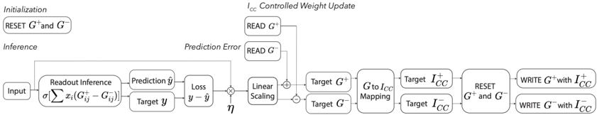
### Visual Description
\n
## Diagram: I<sub>CC</sub> Controlled Weight Update
### Overview
The image is a diagram illustrating the process of I<sub>CC</sub> (presumably, "Input-Controlled Computation") Controlled Weight Update. It depicts a feedback loop involving inference, prediction error calculation, and weight updates based on the error. The diagram is structured horizontally, with an "Initialization" section on the left and a "I<sub>CC</sub> Controlled Weight Update" section on the right. A central "Inference" pathway connects these two sections.
### Components/Axes
The diagram consists of several rectangular blocks representing operations or data storage. Key labels include:
* **Initialization:** "RESET G<sup>+</sup> and G<sup>-</sup>"
* **Inference:** "Input", "Readout Inference", "Prediction ŷ", "Loss", "Linear Scaling", "Target G<sup>+</sup>", "Target G<sup>-</sup>", "Target I<sub>CC</sub>"
* **I<sub>CC</sub> Controlled Weight Update:** "I<sub>CC</sub> Controlled Weight Update", "READ G<sup>+</sup>", "READ G<sup>-</sup>", "Prediction Error", "Target G<sup>+</sup> to Target I<sub>CC</sub> Mapping", "Target G<sup>-</sup> to Target I<sub>CC</sub> Mapping", "RESET G<sup>+</sup> and G<sup>-</sup>", "WRITE G<sup>+</sup> with I<sub>CC</sub><sup>+</sup>", "WRITE G<sup>-</sup> with I<sub>CC</sub><sup>-</sup>"
* **Mathematical Expressions:** Σ x<sub>i</sub>(G<sub>i</sub><sup>+</sup> - G<sub>i</sub><sup>-</sup>), ŷ - y, η
* **Connections:** Arrows indicate the flow of data and control signals.
### Detailed Analysis or Content Details
The diagram can be broken down into the following steps:
1. **Initialization:** The process begins with resetting the weights G<sup>+</sup> and G<sup>-</sup>.
2. **Inference:**
* An "Input" is fed into a "Readout Inference" block, which calculates a weighted sum: Σ x<sub>i</sub>(G<sub>i</sub><sup>+</sup> - G<sub>i</sub><sup>-</sup>).
* This results in a "Prediction" ŷ.
* A "Loss" is calculated as the difference between the prediction ŷ and the "Target" y (ŷ - y).
* The "Loss" is then subjected to "Linear Scaling" with a coefficient η.
3. **I<sub>CC</sub> Controlled Weight Update:**
* The scaled "Prediction Error" is used to compute "Target G<sup>+</sup>" and "Target G<sup>-</sup>".
* These targets are then mapped to "Target I<sub>CC</sub>" using "Target G<sup>+</sup> to Target I<sub>CC</sub> Mapping" and "Target G<sup>-</sup> to Target I<sub>CC</sub> Mapping".
* "READ G<sup>+</sup>" and "READ G<sup>-</sup>" are performed.
* Finally, the weights G<sup>+</sup> and G<sup>-</sup> are updated by writing I<sub>CC</sub><sup>+</sup> and I<sub>CC</sub><sup>-</sup> respectively.
* The process then loops back to the "Inference" stage after resetting G<sup>+</sup> and G<sup>-</sup>.
### Key Observations
The diagram highlights a closed-loop system where the prediction error drives the weight updates. The use of separate weights G<sup>+</sup> and G<sup>-</sup> suggests a mechanism for representing positive and negative influences or features. The "I<sub>CC</sub>" component appears to be a crucial element in controlling the weight update process, potentially providing a way to regulate the magnitude or direction of the updates.
### Interpretation
This diagram illustrates a learning algorithm, likely a form of gradient descent or a related optimization technique. The "I<sub>CC</sub>" component suggests a more sophisticated weight update rule than standard gradient descent, potentially incorporating input-dependent or context-aware adjustments. The feedback loop ensures that the weights are iteratively refined to minimize the prediction error. The separation of weights into G<sup>+</sup> and G<sup>-</sup> could represent a form of feature selection or a mechanism for handling opposing influences. The diagram suggests a system designed for adaptive learning, where the weight updates are dynamically adjusted based on the input and the prediction error. The use of "Target" values implies a supervised learning setting, where the algorithm is trained to match a desired output. The overall architecture suggests a system capable of learning complex relationships between inputs and outputs.
</details>
supplementary note 5 During the inference procedure, reservoir output vector of length 30 is fed into the readout layer. Memristors in the readout layer are placed in the differential architecture, in which the difference of conductance values of two differential memristors ( G + and G -) determines the effective synaptic strength. Scaled with β = 1/ ( G max -G min ) , where G max = 0.35mS and G min = 0.1mS, the weight matrix ( 30 × 4 ) is calculated as W = β [ G + -G -] . And the network prediction is determined by choosing output neuron index with the maximum activation level.
For the training procedure, the network loss is calculated as the difference between output layer prediction and the one-hot encoded target vector indicating one of the four firing patterns. At this point, one can calculate targeted weights using the backpropagation algorithm. However, to support fully online-learning, we tested Icc controlled weight update scheme where following stages in the pipeline can be easily implemented with the mixed-signal circuits in an event-driven manner. The Icc controlled weight update is implemented as follows. First, the required weight change is calculated with W target = η xi δ j , where η is suitably low learning rate, xi is the reservoir layer output and δ j is the calculated error. In order to calculate the target conductance values for both positive and negative memristors, we first linearly scale the weight change to conductance change (by multiplying with 1/ β ). Secondly, we read both the positive and negative conductance values. By using a push-pull mechanism, we calculate the target conductance values. The pushpull mechanism ensures a higher dynamic range in the differential configuration. Third, the target conductances are linearly mapped to the target Icc values ( Icc, target = ( G target + 1.249 × 10 -5 ) / 3 . 338 ) for positive and negative memristors. The weights are updated with the application of RESET and SET pulses with the targeted Icc. Using the linear relation between Icc → G control, we calculated mean ( µ G = 3.338Icc -1.294 × 10 -5 ) and standard deviation σ G = 7.040Icc + 3.0585 and sample from the corresponding Normal distribution.)
F igure A. 32 : 'Reconfigurability' on-the-fly of OGB-capped CsPbBr 3 NC memristors. The device is switched between its non-volatile and volatile mode on demand.
<details>
<summary>Image 70 Details</summary>
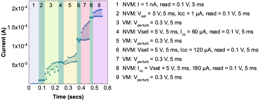
### Visual Description
\n
## Chart: Current vs. Time for NVM Perturbation
### Overview
The image presents a chart illustrating the relationship between current (in Amperes) and time (in seconds) under different perturbation conditions. The chart displays nine distinct data series, each corresponding to a specific perturbation step, labeled 1 through 9. The data appears to represent the current response of a Non-Volatile Memory (NVM) device to varying stimuli.
### Components/Axes
* **X-axis:** Time (secs), ranging from 0 to 0.6 seconds. Marked with tick intervals at 0, 0.1, 0.2, 0.3, 0.4, 0.5, and 0.6.
* **Y-axis:** Current (A), ranging from 0 to 2x10<sup>-4</sup> A (200 µA). Marked with tick intervals at 5x10<sup>-5</sup> A, 1x10<sup>-4</sup> A, and 2x10<sup>-4</sup> A.
* **Data Series:** Nine distinct lines, each representing a different perturbation step, labeled 1-9. Each line is represented by a series of data points connected by lines.
* **Legend:** Located to the right of the chart, listing the conditions for each data series.
### Detailed Analysis
The chart shows a series of current rises and plateaus, each corresponding to a different perturbation step. The data points are plotted as small squares.
* **Series 1 (Green):** Starts at approximately 0 seconds and 5x10<sup>-5</sup> A. The current increases steadily to approximately 1.8x10<sup>-4</sup> A at 0.1 seconds, then plateaus.
* **Series 2 (Light Green):** Begins at 0.1 seconds and 1.8x10<sup>-4</sup> A. The current drops to approximately 5x10<sup>-5</sup> A at 0.2 seconds, then rises again to approximately 1.8x10<sup>-4</sup> A at 0.25 seconds, then plateaus.
* **Series 3 (Yellow):** Starts at 0.2 seconds and 5x10<sup>-5</sup> A. The current remains relatively constant at approximately 5x10<sup>-5</sup> A until 0.3 seconds.
* **Series 4 (Light Yellow):** Begins at 0.3 seconds and 5x10<sup>-5</sup> A. The current increases rapidly to approximately 1.8x10<sup>-4</sup> A at 0.35 seconds, then plateaus.
* **Series 5 (Orange):** Starts at 0.35 seconds and 1.8x10<sup>-4</sup> A. The current drops to approximately 5x10<sup>-5</sup> A at 0.4 seconds, then rises again to approximately 1.8x10<sup>-4</sup> A at 0.45 seconds, then plateaus.
* **Series 6 (Light Orange):** Begins at 0.4 seconds and 5x10<sup>-5</sup> A. The current increases rapidly to approximately 1.8x10<sup>-4</sup> A at 0.45 seconds, then plateaus.
* **Series 7 (Red):** Starts at 0.45 seconds and 5x10<sup>-5</sup> A. The current remains relatively constant at approximately 5x10<sup>-5</sup> A until 0.5 seconds.
* **Series 8 (Light Red):** Begins at 0.5 seconds and 5x10<sup>-5</sup> A. The current increases rapidly to approximately 1.8x10<sup>-4</sup> A at 0.55 seconds, then plateaus.
* **Series 9 (Purple):** Starts at 0.55 seconds and 5x10<sup>-5</sup> A. The current remains relatively constant at approximately 5x10<sup>-5</sup> A until 0.6 seconds.
**Legend Details:**
1. NVM: I = 1 nA, read = 0.1 V, 5 ms
2. NVM: V<sub>set</sub> = 5 V, 5 ms, I<sub>cc</sub> = 1 µA, read = 0.1 V, 5 ms
3. VM: V<sub>perturb</sub> = 0.3 V, 5 ms
4. NVM: V<sub>set</sub> = 5 V, 5 ms, I<sub>cc</sub> = 60 µA, read = 0.1 V, 5 ms
5. VM: V<sub>perturb</sub> = 0.3 V, 5 ms
6. NVM: V<sub>set</sub> = 5 V, 5 ms, I<sub>cc</sub> = 120 µA, read = 0.1 V, 5 ms
7. VM: V<sub>perturb</sub> = 0.3 V, 5 ms
8. NVM: I<sub>cc</sub> = V<sub>set</sub> = 5 V, 5 ms, 180 µA, read = 0.1 V, 5 ms
9. VM: V<sub>perturb</sub> = 0.3 V, 5 ms
### Key Observations
* The chart demonstrates a cyclical pattern of current increase followed by a plateau.
* The current increases are generally rapid, while the plateaus are sustained.
* The perturbation steps 3, 5, 7, and 9 show a relatively constant current level.
* The NVM steps (1, 2, 4, 6, 8) show a similar pattern of current increase and plateau, but with varying current levels.
* The current levels appear to be correlated with the I<sub>cc</sub> values in the NVM steps. Higher I<sub>cc</sub> values generally correspond to higher current plateaus.
### Interpretation
The data suggests that the NVM device exhibits a current response that is sensitive to the applied perturbation conditions. The alternating steps of NVM and VM perturbation likely represent a read/write cycle or a similar operation. The current increases likely correspond to the writing process, while the plateaus represent the reading process. The varying I<sub>cc</sub> values in the NVM steps indicate that the current response can be controlled by adjusting the current compliance. The VM perturbation steps, with a constant V<sub>perturb</sub>, likely serve as a baseline or control condition. The cyclical nature of the data suggests that the device is capable of repeated read/write cycles. The data could be used to characterize the performance of the NVM device and optimize its operating parameters. The consistent V<sub>perturb</sub> values across steps 3, 5, 7, and 9 suggest a consistent baseline for comparison against the NVM steps.
</details>
supplementary note 6 To demonstrate "reconfigurability" on-the-fly, our devices are switched between volatile and non-volatile modes with precise compliance current ( Icc ) con-
trol and selection of activation voltages. Fig. A. 32 shows that our devices can act as a volatile memory even after setting it to multiple non-volatile states. This proves true "reconfigurability" of our devices, hitherto undemonstrated. Such behaviour is an example of the neuromorphic implementation of synapses in Spiking Neural Networks (SNNs) that demand both volatile and non-volatile switching properties, simultaneously.
- 1 . McCulloch, W. S. & Pitts, W. A logical calculus of the ideas immanent in nervous activity. Bulletin of Mathematical Biophysics 5 , 115 ( 4 1943 ).
- 2 . Turing, A. M. I.-computing machinery and intelligence. Mind LIX , 433 ( 236 1950 ).
- 3 . P., H. & von Neumann, J. The computer and the brain. Mathematical Tables and Other Aids to Computation 13 , 226 ( 67 1959 ).
- 4 . Tagkopoulos, I., Liu, Y.-C. & Tavazoie, S. Predictive behavior within microbial genetic networks. Science 320 , 1313 ( 5881 2008 ).
- 5 . Chiang, W.-L., Zheng, L., Sheng, Y., Angelopoulos, A. N., Li, T., Li, D., Zhang, H., Zhu, B., Jordan, M., Gonzalez, J. E. & Stoica, I. Chatbot Arena: An open platform for evaluating LLMs by human preference. arXiv [cs.AI] ( 2024 ).
- 6 . Marr, D. Vision: A computational investigation into the human representation and processing of visual information 429 pp. (MIT Press, London, England, 2010 ).
- 7 . Richards, B. A., Lillicrap, T. P., Beaudoin, P., Bengio, Y., Bogacz, R., Christensen, A., Clopath, C., Costa, R. P., Berker, A. d., Ganguli, S., Gillon, C. J., Hafner, D., Kepecs, A., Kriegeskorte, N., Latham, P., Lindsay, G. W., Miller, K. D., Naud, R., Pack, C. C., Poirazi, P., Roelfsema, P., Sacramento, J., Saxe, A., Scellier, B., Schapiro, A. C., Senn, W., Wayne, G., Yamins, D., Zenke, F., Zylberberg, J., Therien, D. & Kording, K. P. A deep learning framework for neuroscience. Nature Neuroscience 22 , 1761 ( 2019 ).
- 8 . Braitenberg, V. & Schüz, A. in Cortex: Statistics and Geometry of Neuronal Connectivity 51 (Springer Berlin Heidelberg, Berlin, Heidelberg, 1998 ).
- 9 . OpenAI et al. GPT4 Technical Report. arXiv [cs.CL] ( 2023 ).
- 10 . Henighan, T., Kaplan, J., Katz, M., Chen, M., Hesse, C., Jackson, J., Jun, H., Brown, T. B., Dhariwal, P., Gray, S., Hallacy, C., Mann, B., Radford, A., Ramesh, A., Ryder, N., Ziegler, D. M., Schulman, J., Amodei, D. & McCandlish, S. Scaling laws for autoregressive generative modeling. arXiv [cs.LG] ( 2020 ).
- 11 . Horowitz, M. 1 . 1 Computing's Energy Problem (and what we can do about it) in 2014 IEEE International Solid-State Circuits Conference Digest of Technical Papers (ISSCC) 2014 IEEE International Solid-State Circuits Conference Digest of Technical Papers (ISSCC) ( 2014 ), 10 .
- 12 . Boroumand, A., Ghose, S., Akin, B., Narayanaswami, R., Oliveira, G. F., Ma, X., Shiu, E. & Mutlu, O. Google neural network models for edge devices: Analyzing and mitigating machine learning inference bottlenecks in 2021 30 th International Conference on Parallel Architectures and Compilation Techniques (PACT) 2021 30 th International Conference on Parallel Architectures and Compilation Techniques (PACT)Atlanta, GA, USA (IEEE, 2021 ), 159 .
- 13 . Chua, L. Memristor-The missing circuit element. IEEE Trans. Circuit Theory 18 , 507 ( 5 1971 ).
- 14 . Le Gallo, M., Sebastian, A., Mathis, R., Manica, M., Giefers, H., Tuma, T., Bekas, C., Curioni, A. & Eleftheriou, E. Mixed-precision in-memory computing. Nat. Electron. 1 , 246 ( 4 2018 ).
- 15 . Bartol, T. M., Bromer, C., Kinney, J., Chirillo, M. A., Bourne, J. N., Harris, K. M. & Sejnowski, T. J. Nanoconnectomic upper bound on the variability of synaptic plasticity. Elife 4 , e 10778 ( 2015 ).
- 16 . Burr, G. W., Shelby, R. M., Sebastian, A., Kim, S., Kim, S., Sidler, S., Virwani, K., Ishii, M., Narayanan, P., Fumarola, A., Sanches, L. L., Boybat, I., Le Gallo, M., Moon, K., Woo, J., Hwang, H. & Leblebici, Y. Neuromorphic computing using non-volatile memory. Adv. Phys. X. 2 , 89 ( 1 2017 ).
- 17 . Demirag, Y. Multiphysics modeling of Ge 2 Sb 2 Te 5 based synaptic devices for brain inspired computing MA thesis (Ihsan Dogramaci Bilkent University, Ankara, Turkey, 2018 ).
- 18 . Wan, W., Kubendran, R., Schaefer, C., Eryilmaz, S. B., Zhang, W., Wu, D., Deiss, S., Raina, P., Qian, H., Gao, B., et al. A compute-in-memory chip based on resistive random-access memory. Nature 608 , 504 ( 2022 ).
- 19 . Chanthbouala, A., Garcia, V., Cherifi, R. O., Bouzehouane, K., Fusil, S., Moya, X., Xavier, S., Yamada, H., Deranlot, C., Mathur, N. D., Bibes, M., Barthélémy, A. & Grollier, J. A ferroelectric memristor. Nat. Mater. 11 , 860 ( 10 2012 ).
- 20 . Lu, S. & Sengupta, A. Exploring the connection between binary and Spiking Neural Networks. Front. Neurosci. 14 , 535 ( 2020 ).
- 21 . John, R. A., Acharya, J., Zhu, C., Surendran, A., Bose, S. K., Chaturvedi, A., Tiwari, N., Gao, Y., He, Y., Zhang, K. K., Xu, M., Leong, W. L., Liu, Z., Basu, A. & Mathews, N. Optogenetics inspired transition metal dichalcogenide neuristors for in-memory deep recurrent neural networks. Nat. Commun. 11 , 3211 ( 1 2020 ).
- 22 . Sidler, S., Boybat, I., Shelby, R. M., Narayanan, P., Jang, J., Fumarola, A., Moon, K., Leblebici, Y., Hwang, H. & Burr, G. W. Large-scale neural networks implemented with Non-Volatile Memory as the synaptic weight element: Impact of conductance response in 2016 46 th European Solid-State Device Research Conference (ESSDERC) ESSDERC 2016 -46 th European Solid-State Device Research ConferenceLausanne, Switzerland (IEEE, 2016 ), 440 .
- 23 . Khaddam-Aljameh, R., Stanisavljevic, M., Mas, J. F., Karunaratne, G., Brändli, M., Liu, F., Singh, A., Müller, S. M., Egger, U., Petropoulos, A., Antonakopoulos, T., Brew, K., Choi, S., Ok, I., Lie, F. L., Saulnier, N., Chan, V ., Ahsan, I., Narayanan, V., Nandakumar, S. R., Le Gallo, M., Francese, P. A., Sebastian, A. & Eleftheriou, E. HERMES-Core-A 1 . 59 -TOPS/mm 2 PCM on 14 -nm CMOS In-Memory Compute Core Using 300 -ps/LSB Linearized CCO-Based ADCs. IEEE J. Solid-State Circuits , 1 ( 2022 ).
- 24 . Berdan, R., Vasilaki, E., Khiat, A., Indiveri, G., Serb, A. & Prodromakis, T. Emulating short-term synaptic dynamics with memristive devices. Sci. Rep. 6 , 18639 ( 1 2016 ).
- 25 . Ohno, T., Hasegawa, T., Tsuruoka, T., Terabe, K., Gimzewski, J. K. & Aono, M. Short-term plasticity and long-term potentiation mimicked in single inorganic synapses. Nat. Mater. 10 , 591 ( 8 2011 ).
- 26 . Zhang, X., Wang, W., Liu, Q., Zhao, X., Wei, J., Cao, R., Yao, Z., Zhu, X., Zhang, F., Lv, H., Long, S. & Liu, M. An artificial neuron based on a threshold switching memristor. IEEE Electron Device Lett. 39 , 308 ( 2 2018 ).
- 27 . Huang, H.-M., Yang, R., Tan, Z.-H., He, H.-K., Zhou, W., Xiong, J. & Guo, X. Quasi-HodgkinHuxley neurons with leaky integrate-and-fire functions physically realized with memristive devices. Adv. Mater. 31 , e 1803849 ( 3 2019 ).
- 28 . Dalgaty, T., Moro, F., Demirag, Y., De Pra, A., Indiveri, G., Vianello, E. & Payvand, M. Mosaic: in-memory computing and routing for small-world spike-based neuromorphic systems. Nat. Commun. 15 , 1 ( 1 2024 ).
- 29 . Indiveri, G., Linares-Barranco, B., Hamilton, T., van Schaik, A., Etienne-Cummings, R., Delbruck, T., Liu, S.-C., Dudek, P., Häfliger, P., Renaud, S., Schemmel, J., Cauwenberghs, G., Arthur, J., Hynna, K., Folowosele, F., Saighi, S., Serrano-Gotarredona, T., Wijekoon, J., Wang, Y. & Boahen, K. Neuromorphic silicon neuron circuits. Frontiers in Neuroscience 5 , 1 ( 2011 ).
- 30 . Sterling, P. in Principles of Neural Design 155 (The MIT Press, 2015 ).
- 31 . Liu, S.-C., Van Schaik, A., Minch, B. A. & Delbruck, T. Event-based 64 -channel binaural silicon cochlea with Q enhancement mechanisms in 2010 IEEE International Symposium on Circuits and Systems (ISCAS) ( 2010 ), 2027 .
- 32 . Rueckauer, B. & Delbruck, T. Evaluation of event-based algorithms for optical flow with ground-truth from inertial measurement sensor. Front. Neurosci. 10 , 176 ( 2016 ).
- 33 . Mahowald, M. VLSI analogs of neuronal visual processing: a synthesis of form and function ( 1992 ).
- 34 . Boahen, K. Dendrocentric learning for synthetic intelligence. Nature 612 , 43 ( 7938 2022 ).
- 35 . Kubke, M. F., Massoglia, D. P. & Carr, C. E. Developmental changes underlying the formation of the specialized time coding circuits in barn owls (Tyto alba). J. Neurosci. 22 , 7671 ( 17 2002 ).
- 36 . O'Keefe, J. & Recce, M. L. Phase relationship between hippocampal place units and the EEG theta rhythm. Hippocampus 3 , 317 ( 3 1993 ).
- 37 . MacKay, D. M. & McCulloch, W. S. The limiting information capacity of a neuronal link. Bulletin of Mathematical Biophysics 14 , 127 ( 2 1952 ).
- 38 . Aceituno, P. V., de Haan, S., Loidl, R. & Grewe, B. F. Hierarchical target learning in the mammalian neocortex: A pyramidal neuron perspective. bioRxiv ( 2024 ).
- 39 . Payeur, A., Guerguiev, J., Zenke, F., Richards, B. A. & Naud, R. Burst-dependent synaptic plasticity can coordinate learning in hierarchical circuits. bioRxiv ( 2020 ).
- 40 . Gerstner, W., Kempter, R., van Hemmen, J. L. & Wagner, H. A neuronal learning rule for sub-millisecond temporal coding. Nature 383 , 76 ( 6595 1996 ).
- 41 . Demirag, Y. & Indiveri, G. Network of biologically plausible neuron models can solve motor tasks through heterogeneity in Computational and Systems Neuroscience (COSYNE) (Lisbon, Portugal, 2024 ).
- 42 . Hardtdegen, A., La Torre, C., Cuppers, F., Menzel, S., Waser, R. & Hoffmann-Eifert, S. Improved switching stability and the effect of an internal series resistor in HfO 2 /TiO<italic>x</italic> bilayer ReRAM cells. IEEE Trans. Electron Devices 65 , 3229 ( 8 2018 ).
- 43 . Nandakumar, S. R., Boybat, I., Han, J.-P., Ambrogio, S., Adusumilli, P., Bruce, R. L., BrightSky, M., Rasch, M., Le Gallo, M. & Sebastian, A. Precision of synaptic weights programmed in phase-change memory devices for deep learning inference in 2020 IEEE International Electron Devices Meeting (IEDM) 2020 IEEE International Electron Devices Meeting (IEDM)San Francisco, CA, USA (IEEE, 2020 ), 29 . 4 . 1 .
- 44 . Gong, N., Idé, T., Kim, S., Boybat, I., Sebastian, A., Narayanan, V. & Ando, T. Signal and noise extraction from analog memory elements for neuromorphic computing. Nat. Commun. 9 , 2102 ( 1 2018 ).
- 45 . Gallo, M. L., Kaes, M., Sebastian, A. & Krebs, D. Subthreshold electrical transport in amorphous phase-change materials. New Journal of Physics 17 , 093035 ( 2015 ).
- 46 . Burr, G., Shelby, R., Nolfo, C., Jang, J., Shenoy, R., Narayanan, P., Virwani, K., Giacometti, E., Kurdi, B. & Hwang, H. Experimental Demonstration and Tolerancing of a Large-Scale Neural Network ( 165 , 000 Synapses), using Phase-Change Memory as the Synaptic Weight Element. 2014 IEEE International Electron Devices Meeting , 1 ( 2014 ).
- 47 . Stathopoulos, S., Khiat, A., Trapatseli, M., Cortese, S., Serb, A., Valov, I. & Prodromakis, T. Multibit memory operation of metal-oxide bi-layer memristors. Scientific reports 7 , 17532 ( 2017 ).
- 48 . Prezioso, M., Merrikh-Bayat, F., Hoskins, B., Adam, G. C., Likharev, K. K. & Strukov, D. B. Training and operation of an integrated neuromorphic network based on metal-oxide memristors. Nature 521 , 61 ( 2015 ).
- 49 . Bayat, F. M., Prezioso, M., Chakrabarti, B., Nili, H., Kataeva, I. & Strukov, D. Implementation of multilayer perceptron network with highly uniform passive memristive crossbar circuits. Nature communications 9 , 2331 ( 2018 ).
- 50 . Li, C., Hu, M., Li, Y., Jiang, H., Ge, N., Montgomery, E., Zhang, J., Song, W., Dávila, N., Graves, C. E., et al. Analogue signal and image processing with large memristor crossbars. Nature Electronics 1 , 52 ( 2018 ).
- 51 . Boybat, I., Le Gallo, M., Nandakumar, S., Moraitis, T., Parnell, T., Tuma, T., Rajendran, B., Leblebici, Y., Sebastian, A. & Eleftheriou, E. Neuromorphic computing with multimemristive synapses. Nature communications 9 , 2514 ( 2018 ).
- 52 . Agarwal, S., Jacobs Gedrim, R. B., Hsia, A. H., Hughart, D. R., Fuller, E. J., Alec Talin, A., James, C. D., Plimpton, S. J. & Marinella, M. J. Achieving ideal accuracies in analog neuromorphic computing using periodic carry in 2017 Symposium on VLSI Technology (IEEE, 2017 ), T 174 .
- 53 . Suri, M., Bichler, O., Querlioz, D., Palma, G., Vianello, E., Vuillaume, D., Gamrat, C. & DeSalvo, B. CBRAM devices as binary synapses for low-power stochastic neuromorphic systems: auditory (cochlea) and visual (retina) cognitive processing applications in 2012 International Electron Devices Meeting ( 2012 ), 10 .
- 54 . Payvand, M., Muller, L. K. & Indiveri, G. Event-based circuits for controlling stochastic learning with memristive devices in neuromorphic architectures in 2018 IEEE International Symposium on Circuits and Systems (ISCAS) ( 2018 ), 1 .
- 55 . Ambrogio, S., Narayanan, P., Tsai, H., Shelby, R. M., Boybat, I., di Nolfo, C., Sidler, S., Giordano, M., Bodini, M., Farinha, N. C., et al. Equivalent-accuracy accelerated neuralnetwork training using analogue memory. Nature 558 , 60 ( 2018 ).
- 56 . Lillicrap, T. P. & Santoro, A. Backpropagation through time and the brain. Curr. Opin. Neurobiol. Machine Learning, Big Data, and Neuroscience 55 , 82 ( 2019 ).
- 57 . Attneave, F. & Hebb, D. O. The organization of behavior; A neuropsychological theory. Am. J. Psychol. 63 , 633 ( 4 1950 ).
- 58 . Sjöström, P. J., Turrigiano, G. G. & Nelson, S. B. Rate, timing, and cooperativity jointly determine cortical synaptic plasticity. Neuron 32 , 1149 ( 6 2001 ).
- 59 . Feldman, D. E. The spike-timing dependence of plasticity. Neuron 75 , 556 ( 4 2012 ).
- 60 . Oja, E. A simplified neuron model as a principal component analyzer. J. Math. Biol. 15 , 267 ( 3 1982 ).
- 61 . Frenkel, C., Lefebvre, M., Legat, J.-D. & Bol, D. A 0 . 086 -mm 2 12 . 7 -pJ/SOP 64 k-Synapse 256 -Neuron Online-Learning Digital Spiking Neuromorphic Processor in 28 -nm CMOS. IEEE Trans. Biomed. Circuits Syst. 13 , 145 ( 1 2019 ).
- 62 . Frenkel, C., Legat, J.-D. & Bol, D. MorphIC: A 65 -nm 738 k-synapse/mm 2 quad-core binaryweight digital neuromorphic processor with stochastic spike-driven online learning. arXiv [cs.NE] ( 2019 ).
- 63 . Mayr, C., Partzsch, J., Noack, M., Hänzsche, S., Scholze, S., Höppner, S., Ellguth, G. & Schüffny, R. A biological-realtime neuromorphic system in 28 nm CMOS using low-leakage switched capacitor circuits. IEEE Trans. Biomed. Circuits Syst. 10 , 243 ( 1 2016 ).
- 64 . Brader, J. M., Senn, W. & Fusi, S. Learning real-world stimuli in a neural network with spike-driven synaptic dynamics. Neural computation 19 , 2881 ( 2007 ).
- 65 . Marblestone, A. H., Wayne, G. & Kording, K. P. Toward an integration of deep learning and neuroscience. Front. Comput. Neurosci. 10 , 94 ( 2016 ).
- 66 . Laskin, M., Metz, L., Nabarro, S., Saroufim, M., Noune, B., Luschi, C., Sohl-Dickstein, J. & Abbeel, P. Parallel training of deep networks with local updates. arXiv [cs.LG] ( 2020 ).
- 67 . Kaiser, J., Mostafa, H. & Neftci, E. Synaptic plasticity dynamics for Deep Continuous Local Learning (DECOLLE). Front. Neurosci. 14 , 424 ( 2020 ).
- 68 . Rumelhart, D. E., Hinton, G. E. & Williams, R. J. Learning representations by backpropagating errors. Nature 323 , 533 ( 6088 1986 ).
- 69 . Lillicrap, T. P., Cownden, D., Tweed, D. B. & Akerman, C. J. Random synaptic feedback weights support error backpropagation for deep learning. Nat. Commun. 7 , 13276 ( 1 2016 ).
- 70 . Pozzi, I., Bohté, S. & Roelfsema, P. A biologically plausible learning rule for deep learning in the brain. arXiv [cs.NE] ( 2018 ).
- 71 . Lee, D.-H., Zhang, S., Fischer, A. & Bengio, Y. Difference Target Propagation. arXiv [cs.LG] ( 2014 ).
- 72 . Millidge, B., Tschantz, A. & Buckley, C. L. Predictive Coding Approximates Backprop along Arbitrary Computation Graphs. arXiv ( 2020 ).
- 73 . Baydin, A. G., Pearlmutter, B. A., Syme, D., Wood, F. & Torr, P. Gradients without Backpropagation. arXiv [cs.LG] ( 2022 ).
- 74 . Liu, Y. H., Ghosh, A., Richards, B. A., Shea-Brown, E. & Lajoie, G. Beyond accuracy: generalization properties of bio-plausible temporal credit assignment rules. arXiv [cs.NE] ( 2022 ).
- 75 . Bellec, G., Scherr, F., Subramoney, A., Hajek, E., Salaj, D., Legenstein, R. & Maass, W. A solution to the learning dilemma for recurrent networks of spiking neurons. Nature Communications 11 , 1 ( 2020 ).
- 76 . Nagel, M., Fournarakis, M., Amjad, R. A., Bondarenko, Y., van Baalen, M. & Blankevoort, T. A white paper on neural network quantization. arXiv [cs.LG] ( 2021 ).
- 77 . Frenkel, C. & Indiveri, G. ReckOn: A 28 nm sub-mm 2 task-agnostic spiking recurrent neural network processor enabling on-chip learning over second-long timescales. arXiv [cs.NE] ( 2022 ).
- 78 . Lee, J., Kim, D. & Ham, B. Network quantization with element-wise gradient scaling. arXiv [cs.CV] ( 2021 ).
- 79 . Fournarakis, M. & Nagel, M. In-Hindsight Quantization Range Estimation for Quantized Training. 2021 IEEE/CVF Conference on Computer Vision and Pattern Recognition Workshops (CVPRW) , 3057 ( 2021 ).
- 80 . Bernstein, J., Zhao, J., Meister, M., Liu, M.-Y., Anandkumar, A. & Yue, Y. Learning compositional functions via multiplicative weight updates. arXiv [cs.NE] ( 2020 ).
- 81 . Nandakumar, S., Le Gallo, M., Boybat, I., Rajendran, B., Sebastian, A. & Eleftheriou, E. A phase-change memory model for neuromorphic computing. Journal of Applied Physics 124 , 152135 ( 2018 ).
- 82 . Bellec, G., Salaj, D., Subramoney, A., Legenstein, R. & Maass, W. Long short-term memory and learning-to-learn in networks of spiking neurons in Advances in Neural Information Processing Systems ( 2018 ), 787 .
- 83 . Zenke, F. & Neftci, E. O. Brain-Inspired Learning on Neuromorphic Substrates. Proceedings of the IEEE , 1 ( 2021 ).
- 84 . Bohnstingl, T., Wo´ zniak, S., Maass, W., Pantazi, A. & Eleftheriou, E. Online Spatio-Temporal Learning in Deep Neural Networks. arXiv ( 2020 ).
- 85 . Zenke, F. & Ganguli, S. Superspike: Supervised learning in multilayer spiking neural networks. Neural computation 30 , 1514 ( 2018 ).
- 86 . Perez-Nieves, N. & Goodman, D. F. M. Sparse Spiking Gradient Descent. arXiv ( 2021 ).
- 87 . Singh, S. P. & Sutton, R. S. Reinforcement Learning with Replacing Eligibility Traces. Mach. Learn. 22 , 123 ( 1 / 2 / 3 1996 ).
- 88 . Hull, C. L. Principles of Behavior. The Journal of Nervous and Mental Disease 101 , 396 ( 4 1945 ).
- 89 . Davies, M., Srinivasa, N., Lin, T.-H., Chinya, G., Cao, Y., Choday, S. H., Dimou, G., Joshi, P., Imam, N., Jain, S., Liao, Y., Lin, C.-K., Lines, A., Liu, R., Mathaikutty, D., McCoy, S., Paul, A., Tse, J., Venkataramanan, G., Weng, Y.-H., Wild, A., Yang, Y. & Wang, H. Loihi: A neuromorphic manycore processor with on-chip learning. IEEE Micro 38 , 82 ( 2018 ).
- 90 . Grübl, A., Billaudelle, S., Cramer, B., Karasenko, V. & Schemmel, J. Verification and Design Methods for the BrainScaleS Neuromorphic Hardware System. arXiv preprint arXiv: 2003 . 11455 ( 2020 ).
- 91 . Furber, S., Galluppi, F., Temple, S. & Plana, L. The SpiNNaker Project. Proceedings of the IEEE 102 , 652 ( 2014 ).
- 92 . Backus, J. Can programming be liberated from the von Neumann style?: a functional style and its algebra of programs. Communications of the ACM 21 , 613 ( 1978 ).
- 93 . Indiveri, G. & Liu, S.-C. Memory and information processing in neuromorphic systems. Proceedings of the IEEE 103 , 1379 ( 2015 ).
- 94 . Rubino, A., Livanelioglu, C., Qiao, N., Payvand, M. & Indiveri, G. Ultra-low-power FDSOI neural circuits for extreme-edge neuromorphic intelligence. IEEE Trans. Circuits Syst. I Regul. Pap. 68 , 45 ( 1 2021 ).
- 95 . Fuller, E. J., Keene, S. T., Melianas, A., Wang, Z., Agarwal, S., Li, Y., Tuchman, Y., James, C. D., Marinella, M. J., Yang, J. J., Salleo, A. & Talin, A. A. Parallel programming of an ionic floating-gate memory array for scalable neuromorphic computing. Science 364 , 570 ( 6440 2019 ).
- 96 . Huang, Y.-J., Chao, S.-C., Lien, D., Wen, C., He, J.-H. & Lee, S.-C. Dual-functional memory and threshold resistive switching based on the push-pull mechanism of oxygen ions. Sci. Rep. 6 , 23945 ( 1 2016 ).
- 97 . Abbas, H., Abbas, Y., Hassan, G., Sokolov, A. S., Jeon, Y.-R., Ku, B., Kang, C. J. & Choi, C. The coexistence of threshold and memory switching characteristics of ALD HfO 2 memristor synaptic arrays for energy-efficient neuromorphic computing. Nanoscale 12 , 14120 ( 26 2020 ).
- 98 . Kaplan, J., McCandlish, S., Henighan, T., Brown, T. B., Chess, B., Child, R., Gray, S., Radford, A., Wu, J. & Amodei, D. Scaling laws for neural language models. arXiv [cs.LG] ( 2020 ).
- 99 . Prezioso, M., Merrikh-Bayat, F., Hoskins, B., Adam, G., Likharev, K. K. & Strukov, D. B. Training and operation of an integrated neuromorphic network based on metal-oxide memristors. Nature 521 , 61 ( 2015 ).
- 100 . Yao, P., Wu, H., Gao, B., Tang, J., Zhang, Q., Zhang, W., Yang, J. J. & Qian, H. Fully hardware-implemented memristor convolutional neural network. Nature 577 , 641 ( 2020 ).
- 101 . Chen, J., Yang, S., Wu, H., Indiveri, G. & Payvand, M. Scaling Limits of Memristor-Based Routers for Asynchronous Neuromorphic Systems. arXiv preprint arXiv: 2307 . 08116 ( 2023 ).
- 102 . Vianello, E. & Payvand, M. Scaling neuromorphic systems with 3 D technologies. Nat. Electron. 7 , 419 ( 6 2024 ).
- 103 . Moradi, S., Qiao, N., Stefanini, F. & Indiveri, G. A Scalable Multicore Architecture With Heterogeneous Memory Structures for Dynamic Neuromorphic Asynchronous Processors (DYNAPs). Biomedical Circuits and Systems, IEEE Transactions on 12 , 106 ( 2018 ).
- 104 . Sutton, R. S. The Bitter Lesson ( 2024 ).
- 105 . Ielmini, D. Resistive switching memories based on metal oxides: mechanisms, reliability and scaling. Semiconductor Science and Technology 31 , 063002 ( 2016 ).
- 106 . Widrow, B. & Winter, R. Neural nets for adaptive filtering and adaptive pattern recognition. Computer 21 , 25 ( 1988 ).
- 107 . Paszke, A., Gross, S., Massa, F., Lerer, A., Bradbury, J., Chanan, G., Killeen, T., Lin, Z., Gimelshein, N., Antiga, L., Desmaison, A., Kopf, A., Yang, E., DeVito, Z., Raison, M., Tejani, A., Chilamkurthy, S., Steiner, B., Fang, L., Bai, J. & Chintala, S. in Advances in Neural Information Processing Systems 32 (eds Wallach, H., Larochelle, H., Beygelzimer, A., d'Alché-Buc, F., Fox, E. & Garnett, R.) 8024 (Curran Associates, Inc., 2019 ).
- 108 . Bernstein, J., Wang, Y.-X., Azizzadenesheli, K. & Anandkumar, A. signSGD: Compressed Optimisation for Non-Convex Problems. arXiv [cs.LG] ( 2018 ).
- 109 . Boybat, I., Gallo, M. L., Moraitis, T., Parnell, T., Tuma, T., Rajendran, B., Leblebici, Y., Sebastian, A. & Eleftheriou, E. Neuromorphic computing with multi-memristive synapses. Nature Communications 9 , 2514 ( 2018 ).
- 110 . Nandakumar, S. R., Gallo, M. L., Piveteau, C., Joshi, V., Mariani, G., Boybat, I., Karunaratne, G., Khaddam-Aljameh, R., Egger, U., Petropoulos, A., Antonakopoulos, T., Rajendran, B., Sebastian, A. & Eleftheriou, E. Mixed-Precision Deep Learning Based on Computational Memory. Frontiers in Neuroscience 14 , 406 ( 2020 ).
- 111 . Hubara, I., Courbariaux, M., Soudry, D., El-Yaniv, R. & Bengio, Y. Quantized Neural Networks: Training Neural Networks with Low Precision Weights and Activations. arXiv ( 2016 ).
- 112 . Le Gallo, M., Krebs, D., Zipoli, F., Salinga, M. & Sebastian, A. Collective Structural Relaxation in Phase-Change Memory Devices. Advanced Electronic Materials 4 , 1700627 ( 2018 ).
- 113 . Salimans, T., Ho, J., Chen, X., Sidor, S. & Sutskever, I. Evolution Strategies as a Scalable Alternative to Reinforcement Learning. arXiv ( 2017 ).
- 114 . Indiveri, G., Linares-Barranco, B., Legenstein, R., Deligeorgis, G. & Prodromakis, T. Integration of nanoscale memristor synapses in neuromorphic computing architectures. Nanotechnology 24 , 384010 ( 2013 ).
- 115 . Payvand, M., Nair, M. V., Müller, L. K. & Indiveri, G. A neuromorphic systems approach to in-memory computing with non-ideal memristive devices: From mitigation to exploitation. Faraday Discussions 213 , 487 ( 2019 ).
- 116 . Deiss, S., Douglas, R. & Whatley, A. in Pulsed Neural Networks (eds Maass, W. & Bishop, C.) 157 (MIT Press, 1998 ).
- 117 . Alibart, F., Gao, L., Hoskins, B. D. & Strukov, D. B. High precision tuning of state for memristive devices by adaptable variation-tolerant algorithm. Nanotechnology 23 , 075201 ( 2012 ).
- 118 . Nandakumar, S., Le Gallo, M., Boybat, I., Rajendran, B., Sebastian, A. & Eleftheriou, E. Mixed-precision architecture based on computational memory for training deep neural networks in 2018 IEEE International Symposium on Circuits and Systems (ISCAS) ( 2018 ), 1 .
- 119 . Grossi, A., Nowak, E., Zambelli, C., Pellissier, C., Bernasconi, S., Cibrario, G., Hajjam, K. E., Crochemore, R., Nodin, J. F., Olivo, P. & Perniola, L. Fundamental variability limits of filament-based RRAM in 2016 IEEE International Electron Devices Meeting (IEDM) ( 2016 ), 4 . 7 . 1 .
- 120 . Payvand, M. & Indiveri, G. Spike-Based Plasticity Circuits for Always-on On-Line Learning in Neuromorphic Systems in 2019 IEEE International Symposium on Circuits and Systems (ISCAS) (IEEE, Sapporo, Japan, 2019 ), 1 .
- 121 . Delbruck, T. 'Bump' circuits for computing similarity and dissimilarity of analog voltages in Neural Networks, 1991 ., IJCNN91 -Seattle International Joint Conference on 1 ( 1991 ), 475 .
- 122 . Payvand, M., Fouda, M., Kurdahi, F., Eltawil, A. & Neftci, E. O. Error-triggered Three-Factor Learning Dynamics for Crossbar Arrays. arXiv preprint arXiv: 1910 . 06152 ( 2019 ).
- 123 . Goodman, D. Brian: a simulator for spiking neural networks in Python. Frontiers in Neuroinformatics 2 ( 2008 ).
- 124 . Lecun, Y., Bottou, L., Bengio, Y. & Haffner, P. Gradient-based learning applied to document recognition. Proceedings of the IEEE 86 , 2278 ( 1998 ).
- 125 . Dalgaty, T., Payvand, M., Moro, F., Ly, D. R., Pebay-Peyroula, F., Casas, J., Indiveri, G. & Vianello, E. Hybrid neuromorphic circuits exploiting non-conventional properties of RRAM for massively parallel local plasticity mechanisms. APL Materials 7 , 081125 ( 2019 ).
- 126 . Demirag, Y., Frenkel, C., Payvand, M. & Indiveri, G. Online training of spiking recurrent neural networks with Phase-Change Memory synapses 2021 .
- 127 . Demirag, Y., Moro, F., Dalgaty, T., Navarro, G., Frenkel, C., Indiveri, G., Vianello, E. & Payvand, M. PCM-trace: Scalable synaptic eligibility traces with resistivity drift of phase-change materials in 2021 IEEE International Symposium on Circuits and Systems (ISCAS) 2021 IEEE International Symposium on Circuits and Systems (ISCAS)Daegu, Korea. 00 (IEEE, 2021 ), 1 .
- 128 . Bohnstingl, T., Surina, A., Fabre, M., Demirag, Y., Frenkel, C., Payvand, M., Indiveri, G. & Pantazi, A. Biologically-inspired training of spiking recurrent neural networks with neuromorphic hardware in 2022 IEEE 4 th International Conference on Artificial Intelligence Circuits and Systems (AICAS) 2022 IEEE 4 th International Conference on Artificial Intelligence Circuits and Systems (AICAS)Incheon, Korea, Republic of. 00 (IEEE, 2022 ), 218 .
- 129 . Khrulkov, V., Novikov, A. & Oseledets, I. Expressive power of recurrent neural networks. arXiv ( 2017 ).
- 130 . Oord, A. v. d., Dieleman, S., Zen, H., Simonyan, K., Vinyals, O., Graves, A., Kalchbrenner, N., Senior, A. & Kavukcuoglu, K. WaveNet: A Generative Model for Raw Audio. arXiv: 1609 . 03499 [cs] ( 2016 ).
- 131 . Teed, Z. & Deng, J. RAFT: Recurrent All-Pairs Field Transforms for Optical Flow. arXiv ( 2020 ).
- 132 . Brown, T. B., Mann, B., Ryder, N., Subbiah, M., Kaplan, J., Dhariwal, P., Neelakantan, A., Shyam, P., Sastry, G., Askell, A., Agarwal, S., Herbert-Voss, A., Krueger, G., Henighan, T., Child, R., Ramesh, A., Ziegler, D. M., Wu, J., Winter, C., Hesse, C., Chen, M., Sigler, E., Litwin, M., Gray, S., Chess, B., Clark, J., Berner, C., McCandlish, S., Radford, A., Sutskever, I. & Amodei, D. Language Models are Few-Shot Learners. arXiv ( 2020 ).
- 133 . Berner, C., Brockman, G., Chan, B., Cheung, V., Dennison, C., Farhi, D., Fischer, Q., Hashme, S., Hesse, C., Józefowicz, R., Gray, S., Olsson, C., Pachocki, J., Petrov, M., Salimans, T., Schlatter, J., Schneider, J., Sidor, S., Sutskever, I., Tang, J., Wolski, F. & Zhang, S. Dota 2 with Large Scale Deep Reinforcement Learning, 66 ( 2019 ).
- 134 . Ha, D. & Schmidhuber, J. World Models. arXiv: 1803 . 10122 [cs, stat] ( 2018 ).
- 135 . Vinyals, O., Babuschkin, I., Czarnecki, W. M., Mathieu, M., Dudzik, A., Chung, J., Choi, D. H., Powell, R., Ewalds, T., Georgiev, P., Oh, J., Horgan, D., Kroiss, M., Danihelka, I., Huang, A., Sifre, L., Cai, T., Agapiou, J. P., Jaderberg, M., Vezhnevets, A. S., Leblond, R., Pohlen, T., Dalibard, V., Budden, D., Sulsky, Y., Molloy, J., Paine, T. L., Gulcehre, C., Wang, Z., Pfaff, T., Wu, Y., Ring, R., Yogatama, D., Wünsch, D., McKinney, K., Smith, O., Schaul, T., Lillicrap, T., Kavukcuoglu, K., Hassabis, D., Apps, C. & Silver, D. Grandmaster level in StarCraft II using multi-agent reinforcement learning. Nature 575 , 350 ( 2019 ).
- 136 . Douglas, R. & Martin, K. in The synaptic organization of the brain (ed Shepherd, G.) 4 th, 459 (Oxford University Press, Oxford, New York, 1998 ).
- 137 . Douglas, R., Mahowald, M. & Mead, C. Neuromorphic analogue VLSI. Annual Review of Neuroscience 18 , 255 ( 1995 ).
- 138 . Ambrogio, S., Narayanan, P., Tsai, H., Shelby, R. M., Boybat, I., di Nolfo, C., Sidler, S., Giordano, M., Bodini, M., Farinha, N. C. P., Killeen, B., Cheng, C., Jaoudi, Y. & Burr, G. W. Equivalent-accuracy accelerated neural-network training using analogue memory. Nature 558 , 60 ( 2018 ).
- 139 . Li, C., Belkin, D., Li, Y., Yan, P., Hu, M., Ge, N., Jiang, H., Montgomery, E., Lin, P., Wang, Z., Song, W., Strachan, J. P., Barnell, M., Wu, Q., Williams, R. S., Yang, J. J. & Xia, Q. Efficient and self-adaptive in-situ learning in multilayer memristor neural network. Nature Communications 9 , 1 ( 2018 ).
- 140 . Dalgaty, T., Castellani, N., Turck, C., Harabi, K.-E., Querlioz, D. & Vianello, E. In situ learning using intrinsic memristor variability via Markov chain Monte Carlo sampling. Nature Electronics 4 , 151 ( 2021 ).
- 141 . Cai, F., Kumar, S., Van Vaerenbergh, T., Sheng, X., Liu, R., Li, C., Liu, Z., Foltin, M., Yu, S., Xia, Q., et al. Power-efficient combinatorial optimization using intrinsic noise in memristor Hopfield neural networks. Nature Electronics 3 , 409 ( 2020 ).
- 142 . Sebastian, A., Gallo, M. L. & Eleftheriou, E. Computational phase-change memory: beyond von Neumann computing. Journal of Physics D: Applied Physics 52 , 443002 ( 2019 ).
- 143 . Payvand, M., Nair, M. V., Müller, L. K. & Indiveri, G. A neuromorphic systems approach to in-memory computing with non-ideal memristive devices: From mitigation to exploitation. Faraday Discussions 213 , 487 ( 2019 ).
- 144 . Chicca, E. & Indiveri, G. A recipe for creating ideal hybrid memristive-CMOS neuromorphic processing systems. Applied Physics Letters 116 , 120501 ( 2020 ).
- 145 . Peng, X., Huang, S., Luo, Y., Sun, X. & Yu, S. DNN+NeuroSim: An End-to-End Benchmarking Framework for Compute -in-Memory Accelerators with Versatile Device Technologies. IEEE International Electron Devices Meeting (IEDM) , 32 . 5 . 1 ( 2019 ).
- 146 . Peng, X., Huang, S., Jiang, H., Lu, A. & Yu, S. DNN+NeuroSim V 2 . 0 : An End-to-End Benchmarking Framework for Compute-in-Memory Accelerators for On-chip Training. IEEE Transactions on Computer-Aided Design of Integrated Circuits and Systems PP , 1 ( 2020 ).
- 147 . Burr, G. W., Brightsky, M. J., Sebastian, A., Cheng, H.-Y., Wu, J.-Y., Kim, S., Sosa, N. E., Papandreou, N., Lung, H.-L., Pozidis, H., Eleftheriou, E. & Lam, C. H. Recent Progress in Phase-Change Memory Technology. IEEE Journal on Emerging and Selected Topics in Circuits and Systems 6 , 146 ( 2016 ).
- 148 . Burr, G. W., Shelby, R. M., Sebastian, A., Kim, S., Kim, S., Sidler, S., Virwani, K., Ishii, M., Narayanan, P., Fumarola, A., Sanches, L. L., Boybat, I., Le Gallo, M., Moon, K., Woo, J., Hwang, H. & Leblebici, Y. Neuromorphic computing using non-volatile memory. Advances in Physics: X 2 , 89 ( 2017 ).
- 149 . Tuma, T., Pantazi, A., Le Gallo, M., Sebastian, A. & Eleftheriou, E. Stochastic phase-change neurons. Nature Nanotechnology 11 , 693 ( 2016 ).
- 150 . Karunaratne, G., Gallo, M. L., Cherubini, G., Benini, L., Rahimi, A. & Sebastian, A. Inmemory hyperdimensional computing. Nature Electronics 3 , 327 ( 2020 ).
- 151 . Demirag, Y., Moro, F., Dalgaty, T., Navarro, G., Frenkel, C., Indiveri, G., Vianello, E. & Payvand, M. PCM-trace: Scalable Synaptic Eligibility Traces with Resistivity Drift of PhaseChange Materials. 2021 IEEE International Symposium on Circuits and Systems (ISCAS) , 1 ( 2021 ).
- 152 . Gallo, M. L., Sebastian, A., Cherubini, G., Giefers, H. & Eleftheriou, E. Compressed Sensing With Approximate Message Passing Using In-Memory Computing. IEEE Transactions on Electron Devices 65 , 4304 ( 2018 ).
- 153 . Gallo, M. L. & Sebastian, A. An overview of phase-change memory device physics. Journal of Physics D: Applied Physics 53 , 213002 ( 2020 ).
- 154 . Gallo, M. L., Athmanathan, A., Krebs, D. & Sebastian, A. Evidence for thermally assisted threshold switching behavior in nanoscale phase-change memory cells. Journal of Applied Physics 119 , 025704 ( 2016 ).
- 155 . Ielmini, D., Lavizzari, S., Sharma, D. & Lacaita, A. L. Physical Interpretation, Modeling and Impact on Phase Change Memory (PCM) Reliability of Resistance Drift Due to Chalcogenide Structural Relaxation. 2007 IEEE International Electron Devices Meeting , 939 ( 2007 ).
- 156 . Karpov, I., Mitra, M., Kau, D., Spadini, G., Kryukov, Y. & Karpov, V. Fundamental drift of parameters in chalcogenide phase change memory. Journal of Applied Physics 102 , 124503 ( 2007 ).
- 157 . Redaelli, A., Pirovano, A., Benvenuti, A. & Lacaita, A. L. Threshold switching and phase transition numerical models for phase change memory simulations. Journal of Applied Physics 103 , 111101 ( 2008 ).
- 158 . Salinga, M., Carria, E., Kaldenbach, A., Bornhöfft, M., Benke, J., Mayer, J. & Wuttig, M. Measurement of crystal growth velocity in a melt-quenched phase-change material. Nature Communications 4 , 2371 ( 2013 ).
- 159 . Nardone, M., Kozub, V. I., Karpov, I. V. & Karpov, V. G. Possible mechanisms for 1 /f noise in chalcogenide glasses: A theoretical description. Physical Review B 79 , 165206 ( 2009 ).
- 160 . Frémaux, N. & Gerstner, W. Neuromodulated spike-timing-dependent plasticity, and theory of three-factor learning rules. Front. Neur. Circ. 9 , 85 ( 2016 ).
- 161 . Sacramento, J., Costa, R. P., Bengio, Y. & Senn, W. Dendritic cortical microcircuits approximate the backpropagation algorithm in Advances in neural information processing systems ( 2018 ), 8721 .
- 162 . Pozzi, I., Bohté, S. & Roelfsema, P. A Biologically Plausible Learning Rule for Deep Learning in the Brain. arXiv ( 2018 ).
- 163 . Sussillo, D. & Abbott, L. Generating coherent patterns of activity from chaotic neural networks. Neuron 63 , 544 ( 2009 ).
- 164 . Nicola, W. & Clopath, C. Supervised Learning in Spiking Neural Networks with FORCE Training. Nature Communications 8 , 2208 ( 2017 ).
- 165 . Neftci, E. O., Mostafa, H. & Zenke, F. Surrogate gradient learning in spiking neural networks: Bringing the power of gradient-based optimization to spiking neural networks. IEEE Signal Processing Magazine 36 , 51 ( 2019 ).
- 166 . Lee, J. H., Delbruck, T. & Pfeiffer, M. Training Deep Spiking Neural Networks Using Backpropagation. Frontiers in Neuroscience 10 , 508 ( 2016 ).
- 167 . Hochreiter, S. & Schmidhuber, J. Long short-term memory. Neural computation 9 , 1735 ( 1997 ).
- 168 . Qiao, N., Mostafa, H., Corradi, F., Osswald, M., Stefanini, F., Sumislawska, D. & Indiveri, G. A reconfigurable on-line learning spiking neuromorphic processor comprising 256 neurons and 128 K synapses. Frontiers in neuroscience 9 , 141 ( 2015 ).
- 169 . Payvand, M., Muller, L. K. & Indiveri, G. Event-based circuits for controlling stochastic learning with memristive devices in neuromorphic architectures in Circuits and Systems (ISCAS), 2018 IEEE International Symposium on ( 2018 ), 1 .
- 170 . Nair, M. V., Mueller, L. K. & Indiveri, G. A differential memristive synapse circuit for on-line learning in neuromorphic computing systems. Nano Futures 1 , 1 ( 2017 ).
- 171 . Balles, L., Pedregosa, F. & Roux, N. L. The Geometry of Sign Gradient Descent. arXiv ( 2020 ).
- 172 . Nair, M. V. & Dudek, P. Gradient-descent-based learning in memristive crossbar arrays in International Joint Conference on Neural Networks (IJCNN) ( 2015 ), 1 .
- 173 . Müller, L., Nair, M. & Indiveri, G. Randomized Unregulated Step Descent for Limited Precision Synaptic Elements in International Symposium on Circuits and Systems, (ISCAS) ( 2017 ).
- 174 . Payvand, M., Fouda, M. E., Kurdahi, F., Eltawil, A. M. & Neftci, E. O. On-Chip ErrorTriggered Learning of Multi-Layer Memristive Spiking Neural Networks. IEEE Journal on Emerging and Selected Topics in Circuits and Systems 10 , 522 ( 2020 ).
- 175 . Kingma, D. P. & Ba, J. Adam: A method for stochastic optimization. arXiv preprint arXiv: 1412 . 6980 ( 2014 ).
- 176 . Athmanathan, A., Stanisavljevic, M., Papandreou, N., Pozidis, H. & Eleftheriou, E. Multilevel-Cell Phase-Change Memory: A Viable Technology. IEEE Journal on Emerging and Selected Topics in Circuits and Systems 6 , 87 ( 2016 ).
- 177 . Snoek, J., Larochelle, H. & Adams, R. P. Practical Bayesian Optimization of Machine Learning Algorithms in Proceedings of the 25 th International Conference on Neural Information Processing Systems - Volume 2 (Curran Associates Inc., Lake Tahoe, Nevada, 2012 ), 2951 .
- 178 . Davies, M., Wild, A., Orchard, G., Sandamirskaya, Y., Guerra, G. A. F., Joshi, P., Plank, P. & Risbud, S. R. Advancing neuromorphic computing with Loihi: A survey of results and outlook. Proceedings of the IEEE 109 , 911 ( 2021 ).
- 179 . Frenkel, C., Bol, D. & Indiveri, G. Bottom-Up and Top-Down Neural Processing Systems Design: Neuromorphic Intelligence as the Convergence of Natural and Artificial Intelligence. arXiv preprint arXiv: 2106 . 01288 ( 2021 ).
- 180 . Muller, L. K. & Indiveri, G. Rounding methods for neural networks with low resolution synaptic weights. arXiv preprint arXiv: 1504 . 05767 , 1 ( 2015 ).
- 181 . Frenkel, C., Legat, J.-D. & Bol, D. MorphIC: A 65 -nm 738 k-Synapse/mm 2 quad-core binaryweight digital neuromorphic processor with stochastic spike-driven online learning. IEEE Transactions on Biomedical Circuits and Systems 13 , 999 ( 2019 ).
- 182 . Frenkel, C., Legat, J.-D. & Bol, D. A 28 -nm convolutional neuromorphic processor enabling online learning with spike-based retinas in 2020 IEEE International Symposium on Circuits and Systems (ISCAS) ( 2020 ), 1 .
- 183 . Fusi, S. & Abbott, L. Limits on the memory storage capacity of bounded synapses. Nature Neuroscience 10 , 485 ( 2007 ).
- 184 . Laborieux, A., Ernoult, M., Hirtzlin, T. & Querlioz, D. Synaptic metaplasticity in binarized neural networks. Nature communications 12 , 1 ( 2021 ).
- 185 . Khaddam-Aljameh, R., Stanisavljevic, M., Fornt Mas, J., Karunaratne, G., Brandli, M., Liu, F., Singh, A., Muller, S. M., Egger, U., Petropoulos, A., Antonakopoulos, T., Brew, K., Choi, S., Ok, I., Lie, F. L., Saulnier, N., Chan, V ., Ahsan, I., Narayanan, V., Nandakumar, S. R., Le Gallo, M., Francese, P. A., Sebastian, A. & Eleftheriou, E. HERMES-core-A 1 . 59 -TOPS/mm 2 PCM on 14 -nm CMOS in-memory compute core using 300 -ps/LSB linearized CCO-based ADCs. IEEE J. Solid-State Circuits 57 , 1027 ( 4 2022 ).
- 186 . Le Gallo, M., Sebastian, A., Cherubini, G., Giefers, H. & Eleftheriou, E. Compressed Sensing With Approximate Message Passing Using In-Memory Computing. IEEE Trans. Electron Devices 65 , 4304 ( 2018 ).
- 187 . Mead, C. How we created neuromorphic engineering. Nature Electronics 3 , 434 ( 2020 ).
- 188 . Chicca, E., Stefanini, F., Bartolozzi, C. & Indiveri, G. Neuromorphic electronic circuits for building autonomous cognitive systems. Proceedings of the IEEE 102 , 1367 ( 2014 ).
- 189 . Indiveri, G. & Horiuchi, T. Frontiers in Neuromorphic Engineering. Frontiers in Neuroscience 5 , 1 ( 2011 ).
- 190 . Mead, C. Neuromorphic Electronic Systems. Proceedings of the IEEE 78 , 1629 ( 1990 ).
- 191 . Serb, A., Bill, J., Khiat, A., Berdan, R., Legenstein, R. & Prodromakis, T. Unsupervised learning in probabilistic neural networks with multi-state metal-oxide memristive synapses. Nature Communications 7 , 12611 ( 2016 ).
- 192 . Li, Y., Wang, Z., Midya, R., Xia, Q. & Yang, J. J. Review of memristor devices in neuromorphic computing: materials sciences and device challenges. Journal of Physics D: Applied Physics 51 , 503002 ( 2018 ).
- 193 . Spiga, S., Sebastian, A., Querlioz, D. & Rajendran, B. in Memristive Devices for BrainInspired Computing (eds Spiga, S., Sebastian, A., Querlioz, D. & Rajendran, B.) 3 (Woodhead Publishing, 2020 ).
- 194 . Payvand, M. & Indiveri, G. Spike-Based Plasticity Circuits for Always-on On-Line Learning in Neuromorphic Systems in IEEE International Symposium on Circuits and Systems (ISCAS) ( 2019 ), 1 .
- 195 . Widrow, B. & Hoff, M. Adaptive Switching Circuits in 1960 IRE WESCON Convention Record, Part 4 (IRE, New York, 1960 ), 96 .
- 196 . Payvand, M., Fouda, M. E., Kurdahi, F., Eltawil, A. & Neftci, E. O. Error-triggered three-factor learning dynamics for crossbar arrays in International Conference on Artificial Intelligence Circuits and Systems (AICAS) ( 2020 ), 218 .
- 197 . Gerstner, W., Lehmann, M., Liakoni, V., Corneil, D. & Brea, J. Eligibility traces and plasticity on behavioral time scales: experimental support of neohebbian three-factor learning rules. Front. Neur. Circ. 12 , 53 ( 2018 ).
- 198 . Neftci, E. O. Data and Power Efficient Intelligence with Neuromorphic Learning Machines. iScience 5 , 52 ( 2018 ).
- 199 . Sanhueza, M. & Lisman, J. The CaMKII/NMDAR complex as a molecular memory. Molecular brain 6 , 1 ( 2013 ).
- 200 . Rumelhart, D. E., Hinton, G. E. & Williams, R. J. Learning representations by backpropagating errors. Nature 323 , 533 ( 1986 ).
- 201 . Qiao, N., Bartolozzi, C. & Indiveri, G. An Ultralow Leakage Synaptic Scaling Homeostatic Plasticity Circuit With Configurable Time Scales up to 100 ks. IEEE Transactions on Biomedical Circuits and Systems ( 2017 ).
- 202 . Bartolozzi, C. & Indiveri, G. Synaptic dynamics in analog VLSI. Neural Computation 19 , 2581 ( 2007 ).
- 203 . Bartolozzi, C., Mitra, S. & Indiveri, G. An ultra low power current-mode filter for neuromorphic systems and biomedical signal processing in 2006 IEEE Biomedical Circuits and Systems Conference 2006 IEEE Biomedical Circuits and Systems Conference - Healthcare Technology (BioCas)London, UK (IEEE, 2006 ), 130 .
- 204 . Saxena, V. & Baker, R. J. Compensation of CMOS op-amps using split-length transistors in Circuits and Systems (MWSCAS), 2008 IEEE 51 st International Midwest Symposium on ( 2008 ), 109 .
- 205 . Garofolo, John S., Lamel, Lori F., Fisher, William M., Pallett, David S., Dahlgren, Nancy L., Zue, Victor & Fiscus, Jonathan G. TIMIT Acoustic-Phonetic Continuous Speech Corpus 1993 .
- 206 . Cramer, B., Stradmann, Y., Schemmel, J. & Zenke, F. The Heidelberg spiking data sets for the systematic evaluation of spiking neural networks. IEEE Transactions on Neural Networks and Learning Systems ( 2020 ).
- 207 . Xiao, H., Rasul, K. & Vollgraf, R. Fashion-MNIST: A novel image dataset for benchmarking machine learning algorithms. arXiv [cs.LG] ( 2017 ).
- 208 . Orchard, G., Jayawant, A., Cohen, G. K. & Thakor, N. Converting Static Image Datasets to Spiking Neuromorphic Datasets Using Saccades. Frontiers in Neuroscience 9 ( 2015 ).
- 209 . Krizhevsky, A. Learning multiple layers of features from tiny images research rep. ( 2009 ).
- 210 . Deng, J., Dong, W., Socher, R., Li, L.-J., Li, K. & Fei-Fei, L. ImageNet: A large-scale hierarchical image database in 2009 IEEE Conference on Computer Vision and Pattern Recognition (IEEE, 2009 ).
- 211 . Sutton, R. S. & Barto, A. G. Reinforcement learning: an introduction (MIT Press, Cambridge, Mass, 1998 ).
- 212 . Wawrzy´ nski, P. & Tanwani, A. K. Autonomous reinforcement learning with experience replay. Neural Networks 41 , 156 ( 2013 ).
- 213 . Lehmann, M. P., Xu, H. A., Liakoni, V., Herzog, M. H., Gerstner, W. & Preuschoff, K. One-shot learning and behavioral eligibility traces in sequential decision making. Elife 8 , e 47463 ( 2019 ).
- 214 . Lisman, J. A mechanism for the Hebb and the anti-Hebb processes underlying learning and memory. Proc. Natl. Acad. Sci. U. S. A. 86 , 9574 ( 23 1989 ).
- 215 . Shouval, H. Z., Bear, M. F. & Cooper, L. N. A unified model of NMDA receptor-dependent bidirectional synaptic plasticity. Proceedings of the National Academy of Sciences 99 , 10831 ( 16 2002 ).
- 216 . Bosch, M., Castro, J., Saneyoshi, T., Matsuno, H., Sur, M. & Hayashi, Y. Structural and Molecular Remodeling of Dendritic Spine Substructures during Long-Term Potentiation. Neuron 82 , 444 ( 2 2014 ).
- 217 . He, K., Huertas, M., Hong, S. Z., Tie, X., Hell, J. W., Shouval, H. & Kirkwood, A. Distinct Eligibility Traces for LTP and LTD in Cortical Synapses. Neuron 88 , 528 ( 3 2015 ).
- 218 . Brzosko, Z., Schultz, W. & Paulsen, O. Retroactive modulation of spike timing-dependent plasticity by dopamine. eLife 4 , e 09685 ( 2015 ).
- 219 . Ielmini, D., Lavizzari, S., Sharma, D. & Lacaita, A. L. Temperature acceleration of structural relaxation in amorphous Ge 2 Sb 2 Te 5 . Applied Physics Letters 92 , 193511 ( 2008 ).
- 220 . Pirovano, A., Lacaita, A. L., Pellizzer, F., Kostylev, S. A., Benvenuti, A. & Bez, R. Low-field amorphous state resistance and threshold voltage drift in chalcogenide materials. IEEE Transactions on Electron Devices 51 , 714 ( 2004 ).
- 221 . Kim, S., Lee, B., Asheghi, M., Hurkx, F., Reifenberg, J. P., Goodson, K. E. & Wong, H.-S. P. Resistance and threshold switching voltage drift behavior in phase-change memory and their temperature dependence at microsecond time scales studied using a micro-thermal stage. IEEE Transactions on Electron Devices 58 , 584 ( 2011 ).
- 222 . Demirag, Y. Multiphysics modeling of Ge 2 Sb 2 Te 5 based synaptic devices for brain inspired computing MA thesis (Ihsan Dogramaci Bilkent University, Ankara, Turkey, 2018 ).
- 223 . Brader, J. M., Senn, W. & Fusi, S. Learning real-world stimuli in a neural network with spike-driven synaptic dynamics. Neural Computation 19 , 2881 ( 2007 ).
- 224 . Delbruck, T. & Mead, C. Bump circuits in Proceedings of International Joint Conference on Neural Networks 1 ( 1993 ), 475 .
- 225 . Liu, S.-C., Kramer, J., Indiveri, G., Delbruck, T. & Douglas, R. Analog VLSI:Circuits and Principles (MIT Press, 2002 ).
- 226 . Rubino, A., Payvand, M. & Indiveri, G. Ultra-Low Power Silicon Neuron Circuit for ExtremeEdge Neuromorphic Intelligence in International Conference on Electronics, Circuits, and Systems, (ICECS), 2019 ( 2019 ), 458 .
- 227 . Strukov, D. B., Snider, G. S., Stewart, D. R. & Williams, R. S. The missing memristor found. Nature 453 , 80 ( 7191 2008 ).
- 228 . Kumar, S., Williams, R. S. & Wang, Z. Third-order nanocircuit elements for neuromorphic engineering. Nature 585 , 518 ( 7826 2020 ).
- 229 . Grollier, J., Querlioz, D., Camsari, K. Y., Everschor-Sitte, K., Fukami, S. & Stiles, M. D. Neuromorphic spintronics. Nat. Electron. 3 , 360 ( 7 2020 ).
- 230 . Chua, L. Memristor-The missing circuit element. IEEE Trans. Circuit Theory 18 , 507 ( 5 1971 ).
- 231 . Chicca, E., Stefanini, F., Bartolozzi, C. & Indiveri, G. Neuromorphic electronic circuits for building autonomous cognitive systems. Proc. IEEE Inst. Electr. Electron. Eng. 102 . Comment: Submitted to Proceedings of IEEE, spiking neural network implementations in full custom VLSI, 1367 ( 9 2014 ).
- 232 . Cheng, Q., Song, S.-H. & Augustine, G. J. Molecular mechanisms of short-term plasticity: Role of synapsin phosphorylation in augmentation and potentiation of spontaneous glutamate release. Front. Synaptic Neurosci. 10 , 33 ( 2018 ).
- 233 . Boyn, S., Grollier, J., Lecerf, G., Xu, B., Locatelli, N., Fusil, S., Girod, S., Carrétéro, C., Garcia, K., Xavier, S., Tomas, J., Bellaiche, L., Bibes, M., Barthélémy, A., Saïghi, S. & Garcia, V. Learning through ferroelectric domain dynamics in solid-state synapses. Nat. Commun. 8 , 14736 ( 1 2017 ).
- 234 . Wang, Z., Joshi, S., Savel'ev, S. E., Jiang, H., Midya, R., Lin, P., Hu, M., Ge, N., Strachan, J. P., Li, Z., Wu, Q., Barnell, M., Li, G.-L., Xin, H. L., Williams, R. S., Xia, Q. & Yang, J. J. Memristors with diffusive dynamics as synaptic emulators for neuromorphic computing. Nat. Mater. 16 , 101 ( 1 2017 ).
- 235 . Mehonic, A., Sebastian, A., Rajendran, B., Simeone, O., Vasilaki, E. & Kenyon, A. J. Memristors-from in-memory computing, deep learning acceleration, and spiking neural networks to the future of neuromorphic and bio-inspired computing. Adv. Intell. Syst. 2 , 2000085 ( 11 2020 ).
- 236 . Mahmoodi, M. R., Prezioso, M. & Strukov, D. B. Versatile stochastic dot product circuits based on nonvolatile memories for high performance neurocomputing and neurooptimization. Nat. Commun. 10 , 5113 ( 1 2019 ).
- 237 . Karunaratne, G., Le Gallo, M., Cherubini, G., Benini, L., Rahimi, A. & Sebastian, A. Inmemory hyperdimensional computing. Nat. Electron. 3 , 327 ( 6 2020 ).
- 238 . Tuma, T., Pantazi, A., Le Gallo, M., Sebastian, A. & Eleftheriou, E. Stochastic phase-change neurons. Nat. Nanotechnol. 11 , 693 ( 8 2016 ).
- 239 . Appeltant, L., Soriano, M. C., Van der Sande, G., Danckaert, J., Massar, S., Dambre, J., Schrauwen, B., Mirasso, C. R. & Fischer, I. Information processing using a single dynamical node as complex system. Nat. Commun. 2 , 468 ( 1 2011 ).
- 240 . Zhu, X., Wang, Q. & Lu, W. D. Memristor networks for real-time neural activity analysis. Nat. Commun. 11 , 2439 ( 1 2020 ).
- 241 . Ninan, I. & Arancio, O. Presynaptic CaMKII is necessary for synaptic plasticity in cultured hippocampal neurons. Neuron 42 , 129 ( 1 2004 ).
- 242 . Yang, J. J., Strukov, D. B. & Stewart, D. R. Memristive devices for computing. Nat. Nanotechnol. 8 , 13 ( 1 2013 ).
- 243 . Midya, R., Wang, Z., Asapu, S., Joshi, S., Li, Y., Zhuo, Y., Song, W., Jiang, H., Upadhay, N., Rao, M., Lin, P., Li, C., Xia, Q. & Yang, J. J. Artificial neural network (ANN) to spiking neural network (SNN) converters based on diffusive memristors. Adv. Electron. Mater. 5 , 1900060 ( 9 2019 ).
- 244 . Yang, K., Li, F., Veeramalai, C. P. & Guo, T. A facile synthesis of CH 3 NH 3 PbBr 3 perovskite quantum dots and their application in flexible nonvolatile memory. Appl. Phys. Lett. 110 , 083102 ( 8 2017 ).
- 245 . Jeong, J., Kim, M., Seo, J., Lu, H., Ahlawat, P., Mishra, A., Yang, Y., Hope, M. A., Eickemeyer, F. T., Kim, M., Yoon, Y. J., Choi, I. W., Darwich, B. P., Choi, S. J., Jo, Y., Lee, J. H., Walker, B., Zakeeruddin, S. M., Emsley, L., Rothlisberger, U., Hagfeldt, A., Kim, D. S., Grätzel, M. & Kim, J. Y. Pseudo-halide anion engineering for α -FAPbI 3 perovskite solar cells. Nature 592 , 381 ( 7854 2021 ).
- 246 . Hassan, Y., Park, J. H., Crawford, M. L., Sadhanala, A., Lee, J., Sadighian, J. C., Mosconi, E., Shivanna, R., Radicchi, E., Jeong, M., Yang, C., Choi, H., Park, S. H., Song, M. H., De Angelis, F., Wong, C. Y., Friend, R. H., Lee, B. R. & Snaith, H. J. Ligand-engineered bandgap stability in mixed-halide perovskite LEDs. Nature 591 , 72 ( 7848 2021 ).
- 247 . Protesescu, L., Yakunin, S., Bodnarchuk, M. I., Krieg, F., Caputo, R., Hendon, C. H., Yang, R. X., Walsh, A. & Kovalenko, M. V. Nanocrystals of cesium lead Halide perovskites ( CsPbX 3, X = Cl, Br, and I): Novel optoelectronic materials showing bright emission with wide color gamut. Nano Lett. 15 , 3692 ( 6 2015 ).
- 248 . Saidaminov, M. I., Adinolfi, V., Comin, R., Abdelhady, A. L., Peng, W., Dursun, I., Yuan, M., Hoogland, S., Sargent, E. H. & Bakr, O. M. Planar-integrated single-crystalline perovskite photodetectors. Nat. Commun. 6 , 8724 ( 1 2015 ).
- 249 . Yakunin, S., Sytnyk, M., Kriegner, D., Shrestha, S., Richter, M., Matt, G. J., Azimi, H., Brabec, C. J., Stangl, J., Kovalenko, M. V. & Heiss, W. Detection of X-ray photons by solution-processed organic-inorganic perovskites. Nat. Photonics 9 , 444 ( 7 2015 ).
- 250 . Wu, W., Han, X., Li, J., Wang, X., Zhang, Y., Huo, Z., Chen, Q., Sun, X., Xu, Z., Tan, Y., Pan, C. & Pan, A. Ultrathin and conformable lead Halide perovskite photodetector arrays for potential application in retina-like vision sensing. Adv. Mater. 33 , e 2006006 ( 9 2021 ).
- 251 . Xiao, Z. & Huang, J. Energy-efficient hybrid perovskite memristors and synaptic devices. Adv. Electron. Mater. 2 , 1600100 ( 7 2016 ).
- 252 . Xu, W., Cho, H., Kim, Y.-H., Kim, Y.-T., Wolf, C., Park, C.-G. & Lee, T.-W. Organometal Halide perovskite artificial synapses. Adv. Mater. 28 , 5916 ( 28 2016 ).
- 253 . John, R. A., Yantara, N., Ng, Y. F., Narasimman, G., Mosconi, E., Meggiolaro, D., Kulkarni, M. R., Gopalakrishnan, P. K., Nguyen, C. A., De Angelis, F., Mhaisalkar, S. G., Basu, A. & Mathews, N. Ionotronic Halide perovskite drift-diffusive synapses for low-power neuromorphic computation. Adv. Mater. 30 , e 1805454 ( 51 2018 ).
- 254 . Lee, S., Kim, H., Kim, D. H., Kim, W. B., Lee, J. M., Choi, J., Shin, H., Han, G. S., Jang, H. W. & Jung, H. S. Tailored 2 D/ 3 D Halide perovskite heterointerface for substantially enhanced endurance in conducting bridge resistive switching memory. ACS Appl. Mater. Interfaces 12 , 17039 ( 14 2020 ).
- 255 . John, R. A., Yantara, N., Ng, S. E., Patdillah, M. I. B., Kulkarni, M. R., Jamaludin, N. F., Basu, J., Ankit, Mhaisalkar, S. G., Basu, A. & Mathews, N. Diffusive and drift Halide perovskite memristive barristors as nociceptive and synaptic emulators for neuromorphic computing. Adv. Mater. 33 , 2007851 ( 15 2021 ).
- 256 . Tian, H., Zhao, L., Wang, X., Yeh, Y.-W., Yao, N., Rand, B. P. & Ren, T.-L. Extremely low operating current resistive memory based on exfoliated 2 D perovskite single crystals for neuromorphic computing. ACS Nano 11 , 12247 ( 12 2017 ).
- 257 . Wang, Y., Lv, Z., Liao, Q., Shan, H., Chen, J., Zhou, Y., Zhou, L., Chen, X., Roy, V. A. L., Wang, Z., Xu, Z., Zeng, Y.-J. & Han, S.-T. Synergies of electrochemical metallization and valance change in all-inorganic perovskite quantum dots for resistive switching. Adv. Mater. 30 , e 1800327 ( 28 2018 ).
- 258 . Tan, H., Ni, Z., Peng, W., Du, S., Liu, X., Zhao, S., Li, W., Ye, Z., Xu, M., Xu, Y., Pi, X. & Yang, D. Broadband optoelectronic synaptic devices based on silicon nanocrystals for neuromorphic computing. Nano Energy 52 , 422 ( 2018 ).
- 259 . Jarschel, P., Kim, J. H., Biadala, L., Berthe, M., Lambert, Y., Osgood 3 rd, R. M., Patriarche, G., Grandidier, B. & Xu, J. Single-electron tunneling PbS/InP heterostructure nanoplatelets for synaptic operations. ACS Appl. Mater. Interfaces 13 , 38450 ( 32 2021 ).
- 260 . Wang, Y., Lv, Z., Chen, J., Wang, Z., Zhou, Y., Zhou, L., Chen, X. & Han, S.-T. Photonic synapses based on inorganic perovskite quantum dots for neuromorphic computing. Adv. Mater. 30 , e 1802883 ( 38 2018 ).
- 261 . Jiang, T., Shao, Z., Fang, H., Wang, W., Zhang, Q., Wu, D., Zhang, X. & Jie, J. Highperformance nanofloating gate memory based on lead Halide perovskite nanocrystals. ACS Appl. Mater. Interfaces 11 , 24367 ( 27 2019 ).
- 262 . Hao, J., Kim, Y.-H., Habisreutinger, S. N., Harvey, S. P., Miller, E. M., Foradori, S. M., Arnold, M. S., Song, Z., Yan, Y., Luther, J. M. & Blackburn, J. L. Low-energy room-temperature optical switching in mixed-dimensionality nanoscale perovskite heterojunctions. Sci. Adv. 7 ( 18 2021 ).
- 263 . Subramanian Periyal, S., Jagadeeswararao, M., Ng, S. E., John, R. A. & Mathews, N. Halide perovskite quantum dots photosensitized-amorphous oxide transistors for multimodal synapses. Adv. Mater. Technol. 5 , 2000514 ( 11 2020 ).
- 264 . Xiao, X., Hu, J., Tang, S., Yan, K., Gao, B., Chen, H. & Zou, D. Recent advances in Halide perovskite memristors: Materials, structures, mechanisms, and applications. Adv. Mater. Technol. 5 , 1900914 ( 6 2020 ).
- 265 . Xiao, Z., Yuan, Y., Shao, Y., Wang, Q., Dong, Q., Bi, C., Sharma, P., Gruverman, A. & Huang, J. Giant switchable photovoltaic effect in organometal trihalide perovskite devices. Nat. Mater. 14 , 193 ( 2 2015 ).
- 266 . Chen, L.-W., Wang, W.-C., Ko, S.-H., Chen, C.-Y., Hsu, C.-T., Chiao, F.-C., Chen, T.-W., Wu, K.-C. & Lin, H.-W. Highly uniform all-vacuum-deposited inorganic perovskite artificial synapses for reservoir computing. Adv. Intell. Syst. 3 , 2000196 ( 1 2021 ).
- 267 . Midya, R., Wang, Z., Zhang, J., Savel'ev, S. E., Li, C., Rao, M., Jang, M. H., Joshi, S., Jiang, H., Lin, P., Norris, K., Ge, N., Wu, Q., Barnell, M., Li, Z., Xin, H. L., Williams, R. S., Xia, Q. & Yang, J. J. Anatomy of Ag/Hafnia-based selectors with 1010 nonlinearity. Adv. Mater. 29 ( 12 2017 ).
- 268 . Wang, Z., Rao, M., Midya, R., Joshi, S., Jiang, H., Lin, P., Song, W., Asapu, S., Zhuo, Y., Li, C., Wu, H., Xia, Q. & Yang, J. J. Threshold switching of Ag or Cu in dielectrics: Materials, mechanism, and applications. Adv. Funct. Mater. 28 , 1704862 ( 6 2018 ).
- 269 . Guo, M. Q., Chen, Y. C., Lin, C. Y., Chang, Y. F., Fowler, B., Li, Q. Q., Lee, J. & Zhao, Y. G. Unidirectional threshold resistive switching in Au/NiO/Nb:SrTiO 3 devices. Appl. Phys. Lett. 110 , 233504 ( 23 2017 ).
- 270 . Du, C., Cai, F., Zidan, M. A., Ma, W., Lee, S. H. & Lu, W. D. Reservoir computing using dynamic memristors for temporal information processing. Nat. Commun. 8 , 2204 ( 1 2017 ).
- 271 . Gibbons, T. E. Unifying quality metrics for reservoir networks in The 2010 International Joint Conference on Neural Networks (IJCNN) 2010 International Joint Conference on Neural Networks (IJCNN)Barcelona, Spain (IEEE, 2010 ), 1 .
- 272 . Suri, M., Bichler, O., Querlioz, D., Cueto, O., Perniola, L., Sousa, V., Vuillaume, D., Gamrat, C. & DeSalvo, B. Phase change memory as synapse for ultra-dense neuromorphic systems: Application to complex visual pattern extraction in 2011 International Electron Devices Meeting 2011 IEEE International Electron Devices Meeting (IEDM)Washington, DC, USA (IEEE, 2011 ), 4 . 4 . 1 .
- 273 . Hu, M., Strachan, J. P., Li, Z., Grafals, E. M., Davila, N., Graves, C., Lam, S., Ge, N., Yang, J. J. & Williams, R. S. Dot-product engine for neuromorphic computing: programming 1 T 1 Mcrossbar to accelerate matrix-vector multiplication in Proceedings of the 53 rd Annual Design Automation Conference DAC ' 16 : The 53 rd Annual Design Automation Conference 2016 Austin Texas (ACM, New York, NY, USA, 2016 ), 1 .
- 274 . Boybat, I., Le Gallo, M., Nandakumar, S. R., Moraitis, T., Parnell, T., Tuma, T., Rajendran, B., Leblebici, Y., Sebastian, A. & Eleftheriou, E. Neuromorphic computing with multimemristive synapses. Nat. Commun. 9 , 2514 ( 1 2018 ).
- 275 . Sun, X., Wang, N., Chen, C.-Y., Ni, J., Agrawal, A., Cui, X., Venkataramani, S., El Maghraoui, K., Srinivasan, V. ( & Gopalakrishnan, K. Ultra-Low Precision 4 -bit Training of Deep Neural Networks in Advances in Neural Information Processing Systems (eds Larochelle, H., Ranzato, M., Hadsell, R., Balcan, M. F. & Lin, H.) 33 (Curran Associates, Inc., 2020 ), 1796 .
- 276 . Payvand, M., Demirag, Y., Dalgaty, T., Vianello, E. & Indiveri, G. Analog weight updates with compliance current modulation of binary ReRAMs for on-chip learning in 2020 IEEE International Symposium on Circuits and Systems (ISCAS) 2020 IEEE International Symposium on Circuits and Systems (ISCAS)Seville, Spain. 00 (IEEE, 2020 ), 1 .
- 277 . Tanaka, G., Yamane, T., Héroux, J. B., Nakane, R., Kanazawa, N., Takeda, S., Numata, H., Nakano, D. & Hirose, A. Recent advances in physical reservoir computing: A review. Neural Netw. 115 , 100 ( 2019 ).
- 278 . Gerstner, W., Kistler, W. M., Naud, R. & Paninski, L. Neuronal Dynamics: From Single Neurons to Networks and Models of Cognition 590 pp. (Cambridge University Press, Cambridge, England, 2014 ).
- 279 . Watts, D. J. & Strogatz, S. H. Collective dynamics of 'small-world'networks. Nature 393 , 440 ( 1998 ).
- 280 . Kawai, Y., Park, J. & Asada, M. A small-world topology enhances the echo state property and signal propagation in reservoir computing. Neural Networks 112 , 15 ( 2019 ).
- 281 . Loeffler, A., Zhu, R., Hochstetter, J., Li, M., Fu, K., Diaz-Alvarez, A., Nakayama, T., Shine, J. M. & Kuncic, Z. Topological Properties of Neuromorphic Nanowire Networks. Frontiers in Neuroscience 14 , 184 ( 2020 ).
- 282 . Park, H.-J. & Friston, K. Structural and Functional Brain Networks: From Connections to Cognition. Science 342 ( 2013 ).
- 283 . Gallos, L. K., Makse, H. A. & Sigman, M. A small world of weak ties provides optimal global integration of self-similar modules in functional brain networks. Proceedings of the National Academy of Sciences 109 , 2825 ( 2012 ).
- 284 . Sporns, O. & Zwi, J. D. The Small World of the Cerebral Cortex. Neuroinformatics 2 , 145 ( 2004 ).
- 285 . Bullmore, E. & Sporns, O. Complex brain networks: graph theoretical analysis of structural and functional systems. Nature Reviews Neuroscience 10 , 186 ( 2009 ).
- 286 . Bullmore, E. & Sporns, O. Complex brain networks: graph theoretical analysis of structural and functional systems. Nature Reviews Neuroscience 10 , 186 ( 2009 ).
- 287 . Hasler, J. Large-scale field-programmable analog arrays. Proceedings of the IEEE 108 , 1283 ( 2019 ).
- 288 . Jo, S. H., Chang, T., Ebong, I., Bhadviya, B. B., Mazumder, P. & Lu, W. Nanoscale memristor device as synapse in neuromorphic systems. Nano letters 10 , 1297 ( 2010 ).
- 289 . Ielmini, D. & Waser, R. Resistive Switching: From Fundamentals of Nanoionic Redox Processes to Memristive Device Applications (John Wiley & Sons, 2015 ).
- 290 . Strukov, D., Indiveri, G., Grollier, J. & Fusi, S. Building brain-inspired computing. Nature Communications 10 ( 2019 ).
- 291 . Kingra, S. K., Parmar, V., Chang, C.-C., Hudec, B., Hou, T.-H. & Suri, M. SLIM: Simultaneous Logic-In-Memory computing exploiting bilayer analog OxRAM devices. Scientific Reports 10 , 1 ( 2020 ).
- 292 . Wo´ zniak, S., Pantazi, A., Bohnstingl, T. & Eleftheriou, E. Deep learning incorporating biologically inspired neural dynamics and in-memory computing. Nature Machine Intelligence 2 , 325 ( 2020 ).
- 293 . Ambrogio, S., Narayanan, P., Okazaki, A., Fasoli, A., Mackin, C., Hosokawa, K., Nomura, A., Yasuda, T., Chen, A., Friz, A., et al. An analog-AI chip for energy-efficient speech recognition and transcription. Nature 620 , 768 ( 2023 ).
- 294 . Le Gallo, M., Khaddam-Aljameh, R., Stanisavljevic, M., Vasilopoulos, A., Kersting, B., Dazzi, M., Karunaratne, G., Brändli, M., Singh, A., Müller, S. M., et al. A 64 -core mixed-signal inmemory compute chip based on phase-change memory for deep neural network inference. Nature Electronics 6 , 680 ( 2023 ).
- 295 . Sebastian, A., Le Gallo, M., Khaddam-Aljameh, R. & Eleftheriou, E. Memory devices and applications for in-memory computing. Nature Nanotechnology 15 , 529 ( 2020 ).
- 296 . Jouppi, N. P., Young, C., Patil, N., Patterson, D., Agrawal, G., Bajwa, R., Bates, S., Bhatia, S., Boden, N., Borchers, A., et al. In-datacenter performance analysis of a Tensor Processing Unit in Proceedings of the 44 th annual international symposium on computer architecture ( 2017 ), 1 .
- 297 . Yu, S., Sun, X., Peng, X. & Huang, S. Compute-in-memory with emerging nonvolatile-memories: challenges and prospects in 2020 IEEE Custom Integrated Circuits Conference (CICC) ( 2020 ), 1 .
- 298 . Joksas, D., Freitas, P., Chai, Z., Ng, W., Buckwell, M., Li, C., Zhang, W., Xia, Q., Kenyon, A. & Mehonic, A. Committee machines-a universal method to deal with non-idealities in memristor-based neural networks. Nature Communications 11 , 1 ( 2020 ).
- 299 . Zidan, M. A., Strachan, J. P. & Lu, W. D. The future of electronics based on memristive systems. Nature Electronics 1 , 22 ( 2018 ).
- 300 . Mannocci, P., Farronato, M., Lepri, N., Cattaneo, L., Glukhov, A., Sun, Z. & Ielmini, D. In-memory computing with emerging memory devices: Status and outlook. APL Machine Learning 1 ( 2023 ).
- 301 . Duan, S., Hu, X., Dong, Z., Wang, L. & Mazumder, P. Memristor-based cellular nonlinear/neural network: design, analysis, and applications. IEEE Transactions on Neural Networks and Learning Systems 26 , 1202 ( 2014 ).
- 302 . Ascoli, A., Messaris, I., Tetzlaff, R. & Chua, L. O. Theoretical foundations of memristor cellular nonlinear networks: Stability analysis with dynamic memristors. IEEE Transactions on Circuits and Systems I: Regular Papers 67 , 1389 ( 2019 ).
- 303 . Wang, R., Shi, T., Zhang, X., Wei, J., Lu, J., Zhu, J., Wu, Z., Liu, Q. & Liu, M. Implementing insitu self-organizing maps with memristor crossbar arrays for data mining and optimization. Nature Communications 13 , 1 ( 2022 ).
- 304 . Likharev, K., Mayr, A., Muckra, I. & Türel, Ö. CrossNets: High-performance neuromorphic architectures for CMOL circuits. Annals of the New York Academy of Sciences 1006 , 146 ( 2003 ).
- 305 . Betta, G., Graffi, S., Kovacs, Z. M. & Masetti, G. CMOS implementation of an analogically programmable cellular neural network. IEEE Transactions on Circuits and Systems II: Analog and Digital Signal Processing 40 , 206 ( 1993 ).
- 306 . Khacef, L., Rodriguez, L. & Miramond, B. Brain-inspired self-organization with cellular neuromorphic computing for multimodal unsupervised learning. Electronics 9 , 1605 ( 2020 ).
- 307 . Lin, P., Pi, S. & Xia, Q. 3 D integration of planar crossbar memristive devices with CMOS substrate. Nanotechnology 25 , 405202 ( 2014 ).
- 308 . Boahen, K., Nomura, M., Ros Vidal, E. & Van Rullen, R. Address-Event Senders and Receivers: Implementing Direction-Selectivity and Orientation-Tuning (eds Cohen, A., Douglas, R., Horiuchi, T., Indiveri, G., Koch, C., Sejnowski, T. & Shamma, S.) 1998 .
- 309 . Park, J., Yu, T., Joshi, S., Maier, C. & Cauwenberghs, G. Hierarchical address event routing for reconfigurable large-scale neuromorphic systems. IEEE transactions on neural networks and learning systems 28 , 2408 ( 2016 ).
- 310 . Cai, F., Kumar, S., Van Vaerenbergh, T., Sheng, X., Liu, R., Li, C., Liu, Z., Foltin, M., Yu, S., Xia, Q., et al. Power-efficient combinatorial optimization using intrinsic noise in memristor Hopfield neural networks. Nature Electronics 3 , 409 ( 2020 ).
- 311 . Bartolozzi, C. & Indiveri, G. Synaptic dynamics in analog VLSI. Neural computation 19 , 2581 ( 2007 ).
- 312 . Esmanhotto, E., Brunet, L., Castellani, N., Bonnet, D., Dalgaty, T., Grenouillet, L., Ly, D., Cagli, C., Vizioz, C., Allouti, N., et al. High-Density 3 D Monolithically Integrated Multiple 1 T 1 R Multi-Level-Cell for Neural Networks in 2020 IEEE International Electron Devices Meeting (IEDM) ( 2020 ), 36 .
- 313 . Chen, J., Wu, C., Indiveri, G. & Payvand, M. Reliability Analysis of Memristor Crossbar Routers: Collisions and On/off Ratio Requirement in 2022 29 th IEEE International Conference on Electronics, Circuits and Systems (ICECS) ( 2022 ), 1 .
- 314 . Werbos, P. J. Backpropagation through time: What it does and how to do it. Proceedings of the IEEE 78 , 1550 ( 1990 ).
- 315 . Dalgaty, T., Castellani, N., Turck, C., Harabi, K.-E., Querlioz, D. & Vianello, E. In situ learning using intrinsic memristor variability via Markov chain Monte Carlo sampling. Nature Electronics 4 , 151 ( 2021 ).
- 316 . Zhao, M., Wu, H., Gao, B., Zhang, Q., Wu, W., Wang, S., Xi, Y., Wu, D., Deng, N., Yu, S., Chen, H.-Y. & Qian, H. Investigation of statistical retention of filamentary analog RRAM for neuromophic computing in 2017 IEEE International Electron Devices Meeting (IEDM) ( 2017 ), 39 . 4 . 1 .
- 317 . Moro, F., Esmanhotto, E., Hirtzlin, T., Castellani, N., Trabelsi, A., Dalgaty, T., Molas, G., Andrieu, F., Brivio, S., Spiga, S., et al. Hardware calibrated learning to compensate heterogeneity in analog RRAM-based Spiking Neural Networks. IEEE International Symposium in Circuits and Systems ( 2022 ).
- 318 . Moody, G. B. & Mark, R. G. The impact of the MIT-BIH arrhythmia database. IEEE Engineering in Medicine and Biology Magazine 20 , 45 ( 2001 ).
- 319 . Lee, H.-Y., Hsu, C.-M., Huang, S.-C., Shih, Y.-W. & Luo, C.-H. Designing low power of sigma delta modulator for biomedical application. Biomedical Engineering: Applications, Basis and Communications 17 , 181 ( 2005 ).
- 320 . Corradi, F. & Indiveri, G. A neuromorphic event-based neural recording system for smart brain-machine-interfaces. IEEE Transactions on Biomedical Circuits and Systems 9 , 699 ( 2015 ).
- 321 . Brockman, G., Cheung, V., Pettersson, L., Schneider, J., Schulman, J., Tang, J. & Zaremba, W. OpenAI Gym 2016 .
- 322 . Luo, W., Sun, P., Zhong, F., Liu, W., Zhang, T. & Wang, Y. End-to-End Active Object Tracking and Its Real-World Deployment via Reinforcement Learning. IEEE Transactions on Pattern Analysis and Machine Intelligence 42 , 1317 ( 2020 ).
- 323 . Lee, J., Hwangbo, J., Wellhausen, L., Koltun, V. & Hutter, M. Learning quadrupedal locomotion over challenging terrain. Science Robotics 5 ( 2020 ).
- 324 . Vinyals, O., Babuschkin, I., Czarnecki, W. M., Mathieu, M., Dudzik, A., Chung, J., Choi, D. H., Powell, R., Ewalds, T., Georgiev, P., Oh, J., Horgan, D., Kroiss, M., Danihelka, I., Huang, A., Sifre, L., Cai, T., Agapiou, J. P., Jaderberg, M., Vezhnevets, A. S., Leblond, R., Pohlen, T., Dalibard, V., Budden, D., Sulsky, Y., Molloy, J., Paine, T. L., Gulcehre, C., Wang, Z., Pfaff, T., Wu, Y., Ring, R., Yogatama, D., Wünsch, D., McKinney, K., Smith, O., Schaul, T., Lillicrap, T., Kavukcuoglu, K., Hassabis, D., Apps, C. & Silver, D. Grandmaster level in StarCraft II using multi-agent reinforcement learning. Nature 575 , 350 ( 2019 ).
- 325 . OpenAI, Andrychowicz, M., Baker, B., Chociej, M., Jozefowicz, R., McGrew, B., Pachocki, J., Petron, A., Plappert, M., Powell, G., Ray, A., Schneider, J., Sidor, S., Tobin, J., Welinder, P., Weng, L. & Zaremba, W. Learning Dexterous In-Hand Manipulation. arXiv: 1808 . 00177 [cs, stat] ( 2019 ).
- 326 . Jordan, J., Schmidt, M., Senn, W. & Petrovici, M. A. Evolving interpretable plasticity for spiking networks. eLife 10 , e 66273 ( 2021 ).
- 327 . Rabaey, J. M., Chandrakasan, A. P. & Nikoli´ c, B. Digital integrated circuits: a design perspective (Pearson education Upper Saddle River, NJ, 2003 ).
- 328 . Yik, J., Ahmed, S. H., Ahmed, Z., Anderson, B., Andreou, A. G., Bartolozzi, C., Basu, A., Blanken, D. d., Bogdan, P., Bohte, S., et al. NeuroBench: Advancing neuromorphic computing through collaborative, fair and representative benchmarking. arXiv preprint arXiv: 2304 . 04640 ( 2023 ).
- 329 . Merolla, P., Arthur, J., Alvarez, R., Bussat, J.-M. & Boahen, K. A Multicast Tree Router for Multichip Neuromorphic Systems. Circuits and Systems I: Regular Papers, IEEE Transactions on 61 , 820 ( 2014 ).
- 330 . Painkras, E., Plana, L., Garside, J., Temple, S., Galluppi, F., Patterson, C., Lester, D., Brown, A. & Furber, S. SpiNNaker: A 1 -W 18 -Core System-on-Chip for Massively-Parallel Neural Network Simulation. IEEE Journal of Solid-State Circuits 48 , 1943 ( 2013 ).
- 331 . Benjamin, B. V., Gao, P., McQuinn, E., Choudhary, S., Chandrasekaran, A. R., Bussat, J., Alvarez-Icaza, R., Arthur, J., Merolla, P. & Boahen, K. Neurogrid: A Mixed-Analog-Digital Multichip System for Large-Scale Neural Simulations. Proceedings of the IEEE 102 , 699 ( 2014 ).
- 332 . Basu, A., Deng, L., Frenkel, C. & Zhang, X. Spiking neural network integrated circuits: A review of trends and future directions in 2022 IEEE Custom Integrated Circuits Conference (CICC) ( 2022 ), 1 .
- 333 . Pan, X., Ye, T., Xia, Z., Song, S. & Huang, G. Slide-Transformer: Hierarchical Vision Transformer with Local Self-Attention in Proceedings of the IEEE/CVF Conference on Computer Vision and Pattern Recognition ( 2023 ), 2082 .
- 334 . Yu, T., Li, X., Cai, Y., Sun, M. & Li, P. S 2 -mlp: Spatial-shift mlp architecture for vision in Proceedings of the IEEE/CVF winter conference on applications of computer vision ( 2022 ), 297 .
- 335 . Strother, J. A., Nern, A. & Reiser, M. B. Direct observation of ON and OFF pathways in the Drosophila visual system. Current Biology 24 , 976 ( 2014 ).
- 336 . Davies, M., Wild, A., Orchard, G., Sandamirskaya, Y., Guerra, G. A. F., Joshi, P., Plank, P. & Risbud, S. R. Advancing neuromorphic computing with Loihi: A survey of results and outlook. Proceedings of the IEEE 109 , 911 ( 2021 ).
- 337 . Dalgaty, T., Mesquida, T., Joubert, D., Sironi, A., Vivet, P. & Posch, C. HUGNet: Hemi-Spherical Update Graph Neural Network applied to low-latency event-based optical flow in Proceedings of the IEEE/CVF Conference on Computer Vision and Pattern Recognition ( 2023 ), 3952 .
- 338 . Aimone, J. B., Date, P., Fonseca-Guerra, G. A., Hamilton, K. E., Henke, K., Kay, B., Kenyon, G. T., Kulkarni, S. R., Mniszewski, S. M., Parsa, M., et al. A review of non-cognitive applications for neuromorphic computing. Neuromorphic Computing and Engineering 2 , 032003 ( 2022 ).
- 339 . Dalgaty, T., Payvand, M., De Salvo, B., et al. Hybrid CMOS-RRAM neurons with intrinsic plasticity in IEEE ISCAS ( 2019 ), 1 .
- 340 . Joshi, V., Gallo, M. L., Haefeli, S., Boybat, I., Nandakumar, S. R., Piveteau, C., Dazzi, M., Rajendran, B., Sebastian, A. & Eleftheriou, E. Accurate deep neural network inference using computational phase-change memory. Nature Communications 11 ( 2020 ).
- 341 . Corradi, F., Bontrager, D. & Indiveri, G. Toward neuromorphic intelligent brain-machine interfaces: An event-based neural recording and processing system in Biomedical Circuits and Systems Conference (BioCAS) ( 2014 ), 584 .
- 342 . Freeman, C. D., Frey, E., Raichuk, A., Girgin, S., Mordatch, I. & Bachem, O. Brax - A Differentiable Physics Engine for Large Scale Rigid Body Simulation version 0 . 0 . 13 . 2021 .
- 343 . Zucchet, N., Meier, R., Schug, S., Mujika, A. & Sacramento, J. Online learning of long-range dependencies. arXiv [cs.LG] ( 2023 ).
- 344 . Scellier, B. & Bengio, Y. Equilibrium Propagation: Bridging the gap between energy-based models and Backpropagation. Front. Comput. Neurosci. 11 , 24 ( 2017 ).
- 345 . Polimeni, J. M., Mayumi, K., Giampietro, M. & Alcott, B. The Jevons paradox and the myth of resource efficiency improvements 200 pp. (Routledge, London, England, 2012 ).
- 346 . Newman, M. & Watts, D. Renormalization group analysis of the small-world network model. Physics Letters A 263 , 341 ( 1999 ).
- 347 . Zamarreño-Ramos, C., Camuñas-Mesa, L., Pérez-Carrasco, J., Masquelier, T., SerranoGotarredona, T. & Linares-Barranco, B. On spike-timing-dependent-plasticity, memristive devices, and building a self-learning visual cortex. Frontiers in Neuroscience 5 , 1 ( 2011 ).
- 348 . Zhu, X., Lee, J. & Lu, W. D. Iodine vacancy redistribution in organic-inorganic Halide perovskite films and resistive switching effects. Adv. Mater. 29 , 1700527 ( 29 2017 ).
- 349 . Nedelcu, G., Protesescu, L., Yakunin, S., Bodnarchuk, M. I., Grotevent, M. J. & Kovalenko, M. V. Fast anion-exchange in highly luminescent nanocrystals of cesium lead Halide perovskites (CsPbX 3 , X = Cl, Br, I). Nano Lett. 15 , 5635 ( 8 2015 ).
This thesis consists of six selected publications, conducted in collaboration with electrical engineers, computer scientists, material designers and neuroscientists. In this section, I roughly discuss my personal contributions to each project.
## Analog weight updates with compliance current modulation of binary ReRAMs for on-chip learning (Chapter 2 )
- collaborated with material scientists for data collection and modeling (e.g., Fig. 1 )
- coded training and evaluation of RRAM-based neural network simulations (e.g., Alg. 1 )
- assisted circuit design with simulation findings (e.g., Fig. 2 )
- contributed to majority of the manuscript including figures
Online training of spiking recurrent neural networks with Phase-Change Memory synapses (Chapter 3 )
- performed literature review to identify the problem
- coded e-prop, PCM-based analog simulation framework, and neural network training
- conducted all data analysis and visualization
- contributed to majority of the manuscript including figures
## Biologically-inspired training of spiking recurrent neural networks with neuromorphic hardware (Chapter 3 )
- collaboratively planned the project with IBM researchers and INI (e.g., work assignments, experiments, deadlines)
- assisted with experiment datasets, architecture design following prior work [ 126 ]
- weekly supervision of Anja Šurina (e.g., debugging, hyperparameter opt...)
- assisted paper writing and designed several figures
## PCM-trace: scalable synaptic eligibility traces with resistivity drift of Phase-Change Materials (Chapter 3 )
- performed literature review to identify the problem
- collaborated with material scientists for data collection and modeling
- coded pcm-trace and multi-pcm trace experiments and analysis
- assisted circuit design with simulation findings
- contributed to majority of the manuscript
## Reconfigurable halide perovskite nanocrystal memristors for neuromorphic computing (Chapter 4 )
- performed literature review to identify the problem
- collaborated with material scientists for data collection, required device specifications and modeling (e.g. non-volatility time constant, Fig. 4 b-c)
- coded training and evaluation of simulations with volatile and non-volatile memristor models (e.g., RC framework)
- designed ICC modulated training following prior work [ 276 ] (e.g., Supplementary Fig. 28 )
- contributed to majority of the manuscript
Mosaic: in-memory computing and routing for small-world spike-based neuromorphic systems (Chapter 5 )
- performed extensive literature review to identify the strengths the idea
- collaborated with material scientists for data collection and modeling (e.g., Fig. 2 d)
- coded layout-aware training and evaluation of SHD with backprop and RL with ES benchmarks (e.g., Fig. 4 )
- contributed to majority of the manuscript
## Articles in peer-reviewed journals:
- 1 . John, R. A., Demirag, Y., Shynkarenko, Y., Berezovska, Y., Ohannessian, N., Payvand, M., Zeng, P., Bodnarchuk, M. I., Krumeich, F., Kara, G., Shorubalko, I., Nair, M. V., Cooke, G. A., Lippert, T., Indiveri, G. & Kovalenko, M. V. Reconfigurable halide perovskite nanocrystal memristors for neuromorphic computing. Nat. Commun. 13 , 2074 ( 1 2022 ).
- 2 . Dalgaty, T., Moro, F., Demirag, Y., De Pra, A., Indiveri, G., Vianello, E. & Payvand, M. Mosaic: in-memory computing and routing for small-world spike-based neuromorphic systems. Nat. Commun. 15 , 1 ( 1 2024 ).
- 3 . D'Agostino, S., Moro, F., Torchet, T., Demirag, Y., Grenouillet, L., Castellani, N., Indiveri, G., Vianello, E. & Payvand, M. DenRAM: neuromorphic dendritic architecture with RRAM for efficient temporal processing with delays. Nat. Commun. 15 , 1 ( 1 2024 ).
## Preprints:
- 4 . Demirag, Y., Frenkel, C., Payvand, M. & Indiveri, G. Online training of spiking recurrent neural networks with Phase-Change Memory synapses 2021 .
## Conference contributions:
- 5 . Demirag, Y., Moro, F., Dalgaty, T., Navarro, G., Frenkel, C., Indiveri, G., Vianello, E. & Payvand, M. PCM-trace: Scalable synaptic eligibility traces with resistivity drift of phase-change materials in 2021 IEEE International Symposium on Circuits and Systems (ISCAS) 2021 IEEE International Symposium on Circuits and Systems (ISCAS)Daegu, Korea. 00 (IEEE, 2021 ), 1 .
- 6 . Demirag, Y. & Indiveri, G. Network of biologically plausible neuron models can solve motor tasks through heterogeneity in Computational and Systems Neuroscience (COSYNE) (Lisbon, Portugal, 2024 ).
- 7 . Demirag, Y., Dittmann, R., Indiveri, G. & Neftci, E. Overcoming phase-change material nonidealities by meta-learning for adaptation on the edge in Proceedings of Neuromorphic Materials, Devices, Circuits and Systems (NeuMatDeCaS) ( 2023 ).
- 8 . Payvand, M., Demirag, Y., Dalgaty, T., Vianello, E. & Indiveri, G. Analog weight updates with compliance current modulation of binary ReRAMs for on-chip learning in 2020 IEEE International Symposium on Circuits and Systems (ISCAS) 2020 IEEE International Symposium on Circuits and Systems (ISCAS)Seville, Spain. 00 (IEEE, 2020 ), 1 .
- 9 . Bohnstingl, T., Surina, A., Fabre, M., Demirag, Y., Frenkel, C., Payvand, M., Indiveri, G. & Pantazi, A. Biologically-inspired training of spiking recurrent neural networks with neuromorphic hardware in 2022 IEEE 4 th International Conference on Artificial Intelligence Circuits and Systems (AICAS) 2022 IEEE 4 th International Conference on Artificial Intelligence Circuits and Systems (AICAS)Incheon, Korea, Republic of. 00 (IEEE, 2022 ), 218 .
- 10 . Payvand, M., D'Agostino, S., Moro, F., Demirag, Y., Indiveri, G. & Vianello, E. Dendritic computation through exploiting resistive memory as both delays and weights in Proceedings of the 2023 International Conference on Neuromorphic Systems International Conference on Neuromorphic Systems (ICONS) (New York, USA, 2023 ), 1 .
- 11 . Raghunathan, K. C., Demirag, Y., Neftci, E. & Payvand, M. Hardware-aware Few-shot Learning on a Memristor-based Small-world Architecture in Neuro Inspired Computational Elements Conference (NICE) (IEEE, 2024 ).
- 12 . Raghunathan, K. C., Demirag, Y., Moro, F., Neftci, E. & Payvand, M. Few-shot learning on brain-inspired small-world graphical hardware in International Conference on Neuromorphic, Natural and Physical Computing (NNPC 2023 ) (Hannover, Germany, 2023 ).
- 13 . Yu, Z., Bégon-Lours, L., Demirag, Y. & Offrein, B. J. BEOL compatible cross-bar array of ferroelectric synapses in Proceedings of the 2021 International Conference on Neuromorphic Systems International Conference on Neuromorphic Systems (ICONS) ( 2021 ).
- 14 . Yik, J., Ahmed, S. H., Ahmed, Z., Anderson, B., Andreou, A. G., Bartolozzi, C., Basu, A., Blanken, D. d., Bogdan, P., Bohte, S., Bouhadjar, Y., Buckley, S., Cauwenberghs, G., Corradi, F., de Croon, G., Danielescu, A., Daram, A., Davies, M., Demirag, Y., Eshraghian, J., Forest, J., Furber, S., Furlong, M., Gilra, A., Indiveri, G., Joshi, S., Karia, V., Khacef, L., Knight, J. C., Kriener, L., Kubendran, R., Kudithipudi, D., Lenz, G., Manohar, R., Mayr, C., Michmizos, K., Muir, D., Neftci, E., Nowotny, T., Ottati, F., Ozcelikkale, A., Pacik-Nelson, N., Panda, P., Pao-Sheng, S., Payvand, M., Pehle, C., Petrovici, M. A., Posch, C., Renner, A., Sandamirskaya, Y., Schaefer, C. J. S., van Schaik, A., Schemmel, J., Schuman, C., Seo, J.-S., Sheik, S., Shrestha, S. B., Sifalakis, M., Sironi, A., Stewart, K., Stewart, T. C., Stratmann, P., Tang, G., Timcheck, J., Verhelst, M., Vineyard, C. M., Vogginger, B., Yousefzadeh, A., Zhou, B., Zohora, F. T., Frenkel, C. & Reddi, V. J. NeuroBench: Advancing neuromorphic computing through collaborative, fair and representative benchmarking in ( 2023 ).