# All-in-One Analog AI Hardware: On-Chip Training and Inference with Conductive-Metal-Oxide/HfOx ReRAM Devices
**Authors**: \fnmVictoria\surClerico, \fnmWooseok\surChoi, \fnmTommaso\surStecconi, \fnmFolkert\surHorst, \fnmLaura\surBégon-Lours, \fnmMatteo\surGaletta, \fnmAntonio\surLa Porta, \fnmNikhil\surGarg, \fnmFabien\surAlibart, \fnmBert Jan\surOffrein, \fnmValeria\surBragaglia
> dof@zurich.ibm.com
[1] \fnm Donato Francesco \sur Falcone
1] \orgname IBM Research - Europe, \orgaddress \city Rüschlikon, \postcode 8803, \state Zürich, \country Switzerland
2] \orgdiv Institut Interdisciplinaire d’Innovation Technologique (3IT), \orgname Université de Sherbrooke, \orgaddress \city Sherbrooke, \postcode QC J1K 0A5, \state Quebec, \country Canada
3] \orgdiv Institute of Electronics, Microelectronics and Nanotechnology (IEMN), \orgname Université de Lille, \orgaddress \city Villeneuve d’Ascq, \postcode 59650, \country France
Abstract
Analog in-memory computing is an emerging paradigm designed to efficiently accelerate deep neural network workloads. Recent advancements have focused on either inference or training acceleration. However, a unified analog in-memory technology platform—capable of on-chip training, weight retention, and long-term inference acceleration—has yet to be reported. This work presents an all-in-one analog AI accelerator, combining these capabilities to enable energy-efficient, continuously adaptable AI systems. The platform leverages an array of analog filamentary conductive-metal-oxide (CMO)/HfO x resistive switching memory cells (ReRAM) integrated into the back-end-of-line (BEOL). The array demonstrates reliable resistive switching with voltage amplitudes below 1.5 V, compatible with advanced technology nodes. The array’s multi-bit capability (over 32 stable states) and low programming noise (down to 10 nS) enable a nearly ideal weight transfer process, more than an order of magnitude better than other memristive technologies. Inference performance is validated through matrix-vector multiplication simulations on a 64×64 array, achieving a root-mean-square error improvement by a factor of 20 at 1 second and 3 at 10 years after programming, compared to state-of-the-art. Training accuracy closely matching the software equivalent is achieved across different datasets. The CMO/HfO x ReRAM technology lays the foundation for efficient analog systems accelerating both inference and training in deep neural networks.
keywords: In-memory computing, Analog ReRAM, Deep Neural Networks, Training, Inference
1 Introduction
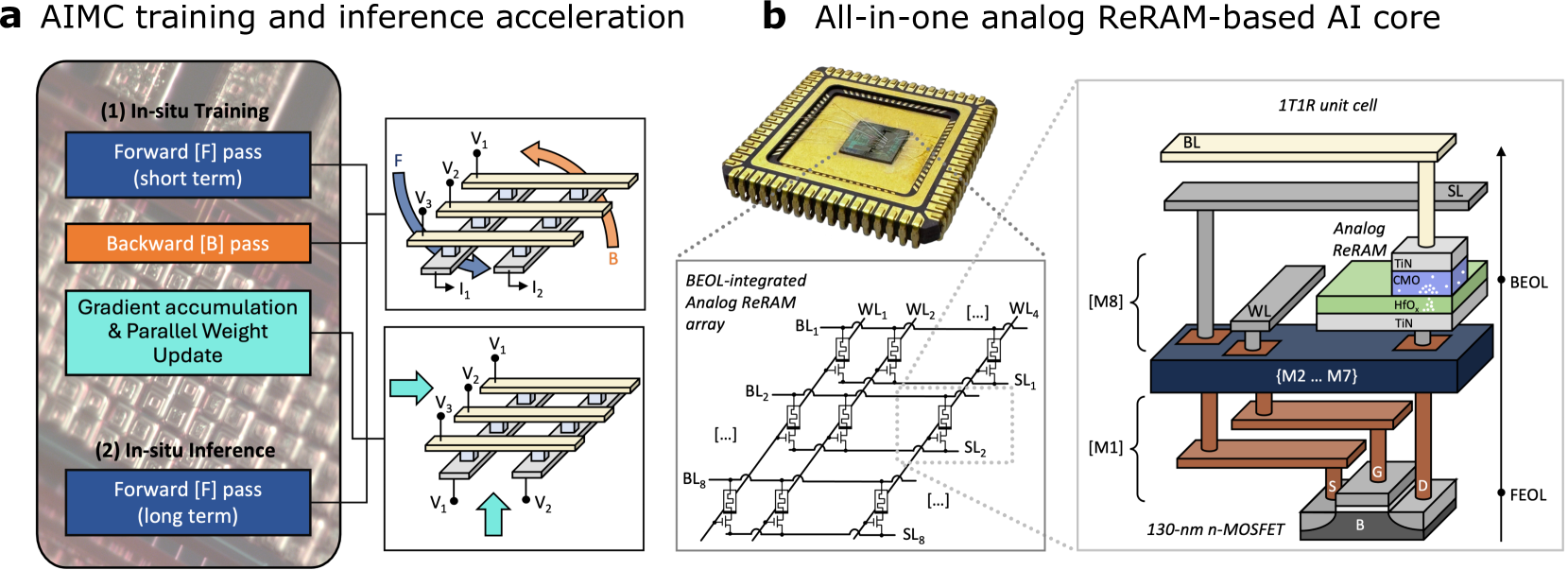
Modern computing systems rely on von Neumann architectures, where instructions and data must be transferred between memory and the processing unit to perform computational tasks. This data transfer, particularly recurrent and massive in prominent artificial intelligence (AI)-related workloads, results in significant latency and energy overhead [1]. Digital AI accelerators address this challenge through computational parallelism, bringing memory closer to the processing units, and exploiting application-specific processors [2, 3]. This approach has demonstrated to bring significant improvements in throughput and efficiency for running deep neural networks (DNNs) [4], but the physical separation between memory and compute units persists. Analog in-memory computing (AIMC) [5] is a promising approach to eliminate this separation and so achieve further power and efficiency improvements in deep-learning workloads [6], by enabling some arithmetic and logic operations to be performed directly at the location where the data is stored. By mapping the weights of DNNs onto crossbar arrays of resistive devices and by leveraging Ohm’s and Kirchhoff’s physical laws, matrix-vector multiplications (MVMs)—the most recurrent operation in AI-workloads [7] —are performed in memory with $O(1)$ time complexity [5, 8, 4]. Recent demonstrations of the AIMC paradigm have primarily focused on accelerating the inference step of digitally trained DNNs [9, 10, 11, 12]. However, the increasing computing demands of modern AI models make the training phase orders of magnitude more costly in time and expenses than inference, highlighting the need for efficient hardware acceleration based on the AIMC paradigm. For instance, Gemini 1.0 Ultra required over $5· 10^{25}$ floating-point operations (FLOPs), approximately 100 days, $\mathrm{24\,MW}$ of power, and an estimated cost of 30 million dollars for training [13]. Analog training acceleration imposes even more stringent requirements on resistive devices. In addition to inference (i.e., the forward pass), the back-propagation of errors, gradient computation, and weight update steps must be performed during the learning phase. However, in the digital domain updating the weights of a matrix of size NxN requires $O(N^{2})$ digital operations, leading to a significant drop in efficiency and speed. Beyond the forward pass, the AIMC approach enables acceleration of (1) backward pass through MVMs transposing the inputs and outputs, (2) gradient computation, and (3) the weight update through gradual bidirectional conductance changes upon external stimuli, all with $O(1)$ time complexity. To achieve this, the ideal analog resistive device should exhibit bidirectional, linear, and symmetric conductance updates in response to an open-loop programming pulse scheme (i.e., without the need for verification following each pulse) [4, 14]. Promising technologies include redox-based resistive switching memory (ReRAM) [15, 16], electro-chemical random access memory (ECRAM) [17], and capacitive weight elements [18]. Addressing the various non-idealities of these technologies [19] requires the co-optimization of technology and designated training algorithms. Gokmen et al. [20] proposed an efficient, fully parallel approach that leverages the coincidence of stochastic voltage pulse trains to carry out outer-product calculations and weight updates entirely within memory, in $O(1)$ time complexity. To relax the device symmetry requirements, a novel training algorithm, known as Tiki-Taka, was designed based on this parallel scheme [21]. The primary advantage of the Tiki-Taka approach lies in reduced device symmetry constraints across the entire conductance (G) range, focusing instead on a localized symmetry point where increases and decreases in G are balanced [21]. More recently, the Tiki-Taka version 2 (TTv2) algorithm was demonstrated in hardware [22] on small-scale tasks using optimized analog ReRAM technology in a 6-Transistor-1ReRAM unit cell crossbar array configuration. However, TTv2 faces some convergence issues when the reference conductance is not programmed with high precision [23]. Analog gradient accumulation with dynamic reference (AGAD) learning algorithm (i.e., TTv4) was proposed to overcome the reference conductance limitation, providing enhanced and robust performance [23]. From a technology perspective, the addition of an engineered conductive-metal-oxide (CMO) layer in a conventional HfO x -based ReRAM metal/insulator/metal (M/I/M) stack has been shown to improve switching characteristics in terms of the number of analog states, stochasticity, symmetry point, and endurance, compared to conventional M/I/M technology [24, 25, 26]. However, while CMO/HfO x ReRAM technology has proven to meet all the fundamental device criteria for on-chip training [24], array-level assessment and BEOL integration remain unexplored. Furthermore, although accelerating DNN training using AIMC is more challenging than inference, a unified technology platform capable of performing on-chip training, retaining the weights, and enabling long-term inference acceleration has yet to be reported. This work fills this gap by demonstrating an all-in-one AI accelerator based on CMO/HfO x ReRAM technology, able to perform analog acceleration of both training and long-term inference operations. Such an integrated approach paves the way for highly autonomous, energy-efficient, and continuously adaptable AI systems, opening new paths for real-time learning and inference applications. The flowchart in Fig. 1 a illustrates the all-in-one analog training and inference challenge addressed in this study. To achieve this goal, CMO/HfO x ReRAM devices, integrated into the BEOL of a $\mathrm{130\,nm}$ complementary metal-oxide-semiconductor (CMOS) technology node with copper interconnects (see ”Methods” section ”Device fabrication” for details), are arranged in an array architecture using a 1T1R unit cell. Compared to implementations that use multiple transistors to control the resistive switching, the 1T1R unit cell maximizes memory density, which is crucial for storing large AI models on a single chip. Fig. 1 b shows an image of the all-in-one analog ReRAM-based AI core used in this work, with the corresponding 8x4 array architecture and the schematic of the BEOL integrated 1T1R cells. The CMO/HfO x ReRAM array is first studied in a quasi-static regime by statistically characterizing the devices’ electro-forming step and quasi-static switching response. A physical 3D finite-element model (FEM) is developed to represent the geometry of the conductive filament and analytically describe the charge transport mechanism within these cells. Subsequently, the weight transfer accuracy and conductance relaxation are experimentally characterized on the 8x4 array. These measurements enable the demonstration of the core’s inference capabilities, validated through representative MVM accuracy simulations on a 64×64 array. After demonstrating the MVM accuracy of the CMO/HfO x ReRAM core, analog switching experiments using an open-loop identical pulse scheme demonstrated the suitability of the same core for analog on-chip training acceleration. To assess the training performance, a realistic device model was used in the simulation, accounting for measured characteristics such as non-linear and asymmetric switching behavior, as well as inter- and intra-device variabilities. The training performance was validated using AGAD on fully connected and long short-term memory (LSTM) neural networks, demonstrating scalability from small to large-scale neural networks.
<details>
<summary>x1.png Details</summary>
### Visual Description
## Diagram: AIMC Training and Inference with ReRAM-based AI Core
### Overview
The image presents a diagram illustrating the acceleration of AI model training and inference using an Analog In-Memory Computing (AIMC) architecture. It highlights the in-situ training and inference processes, along with a detailed view of an all-in-one analog ReRAM-based AI core. The diagram is divided into two main sections: (a) AIMC training and inference acceleration, and (b) All-in-one analog ReRAM-based AI core.
### Components/Axes
**Section a: AIMC training and inference acceleration**
* **(1) In-situ Training:**
* **Forward [F] pass (short term):** Represented by a blue box.
* **Backward [B] pass:** Represented by an orange box.
* **Gradient accumulation & Parallel Weight Update:** Represented by a cyan box.
* **(2) In-situ Inference:**
* **Forward [F] pass (long term):** Represented by a blue box.
* **Diagrams:**
* Top diagram shows the forward pass (F) and backward pass (B) with voltages V1, V2, V3 and currents I1, I2.
* Bottom diagram shows the forward pass with voltages V1, V2, V3.
**Section b: All-in-one analog ReRAM-based AI core**
* **Top-right:** 1T1R unit cell
* BL (Bit Line)
* SL (Source Line)
* Analog ReRAM stack:
* TIN (Titanium Nitride)
* CMO (Conductive Metal Oxide)
* HfOₓ (Hafnium Oxide)
* TIN (Titanium Nitride)
* WL (Word Line)
* {M2 ... M7}
* [M8]
* [M1]
* 130-nm n-MOSFET
* S (Source)
* G (Gate)
* D (Drain)
* B (Body)
* BEOL (Back-End-Of-Line)
* FEOL (Front-End-Of-Line)
* **Bottom-left:** BEOL-integrated Analog ReRAM array
* BL1, BL2, BL8 (Bit Lines)
* WL1, WL2, WL4 (Word Lines)
* SL1, SL2, SL8 (Source Lines)
### Detailed Analysis or ### Content Details
**Section a: AIMC training and inference acceleration**
* The diagram illustrates the flow of data and operations during in-situ training and inference.
* The forward pass is used in both training (short term) and inference (long term).
* The backward pass and gradient accumulation are specific to the training phase.
* The arrows indicate the direction of data flow and the sequence of operations.
**Section b: All-in-one analog ReRAM-based AI core**
* The diagram shows a chip package with the ReRAM-based AI core.
* The ReRAM array is organized in a grid with bit lines (BL), word lines (WL), and source lines (SL).
* The 1T1R unit cell consists of a transistor and a ReRAM element.
* The ReRAM element is composed of TIN, CMO, and HfOₓ layers.
* The diagram highlights the BEOL and FEOL layers in the device.
* The 130-nm n-MOSFET is used as the access transistor for the ReRAM cell.
### Key Observations
* The AIMC architecture integrates training and inference on the same chip.
* The ReRAM-based AI core enables analog in-memory computing.
* The 1T1R unit cell is a fundamental building block of the ReRAM array.
* The diagram provides a detailed view of the device structure and components.
### Interpretation
The diagram illustrates a novel approach to AI acceleration using analog in-memory computing with ReRAM technology. By performing computations directly within the memory array, the AIMC architecture can potentially reduce energy consumption and improve performance compared to traditional digital computing architectures. The integration of training and inference on the same chip enables efficient on-device learning and adaptation. The detailed view of the ReRAM cell and array provides insights into the device structure and operation. The use of HfOₓ as the resistive switching material is a common choice in ReRAM devices due to its good performance and reliability. The 130-nm n-MOSFET provides the necessary switching functionality for accessing and controlling the ReRAM cell. Overall, the diagram highlights the potential of ReRAM-based AIMC for enabling energy-efficient and high-performance AI applications.
</details>
Figure 1: All-in-one AIMC challenge. a Schematic representation of the key steps required to perform on-chip training and inference with analog acceleration. Each step is executed using a crossbar array of resistive devices. b CMO/HfO x ReRAM AI core used in this work, consisting of an 8×4 array of 1T1R unit cells. From a fabrication perspective, each ReRAM cell is integrated into the BEOL of a $\mathrm{130\,nm}$ NMOS transistor with copper interconnects.
2 Results
2.1 Quasi-static array characterization and modelling
The quasi-static electrical characterization and analytical transport modelling of the 8x4 CMO/HfO x ReRAM array are presented here.
2.1.1 Filament forming
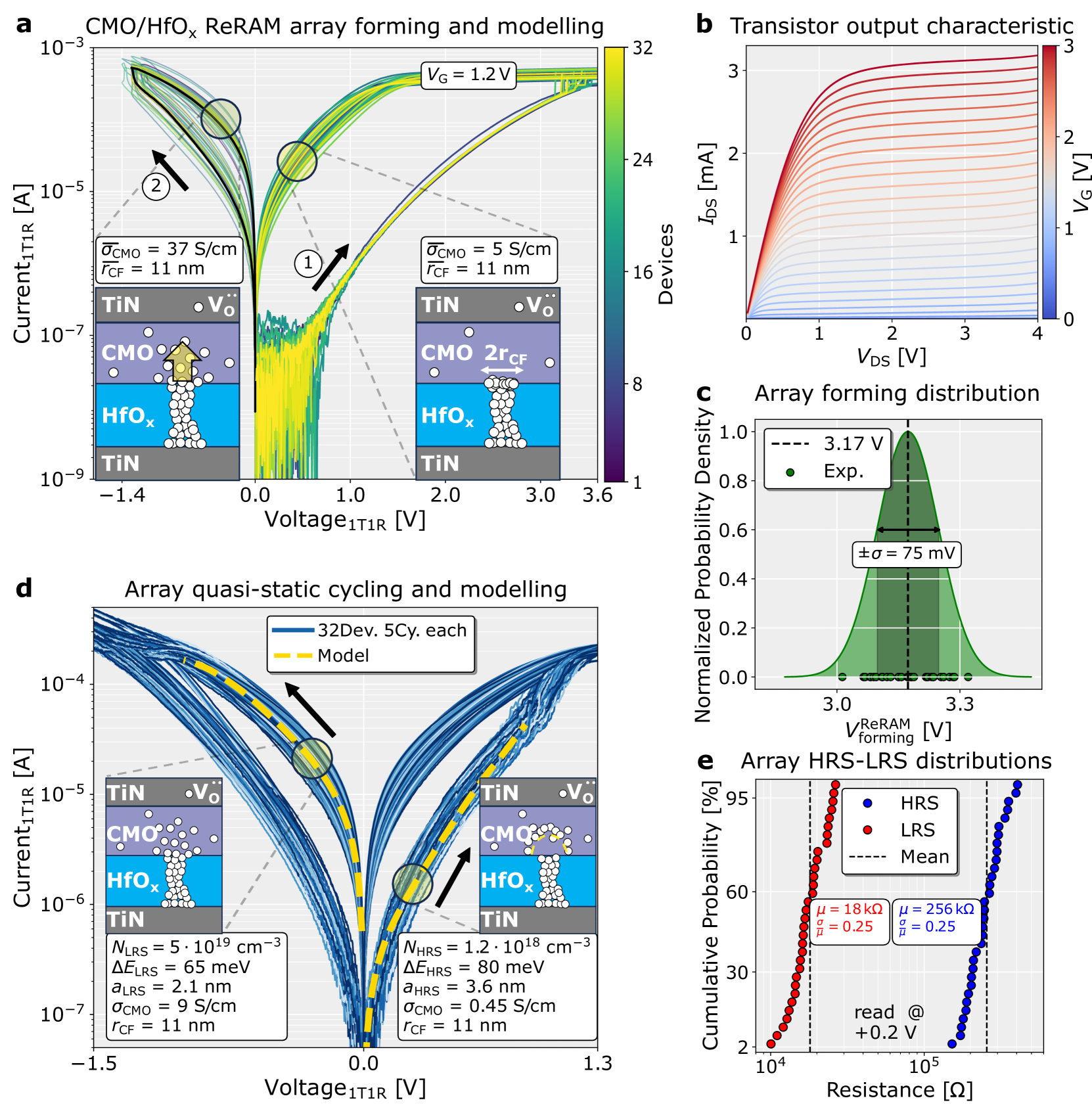
Fig. 2 a shows the current-voltage characteristic of the ReRAM devices in the array, undergoing a soft-dielectric breakdown process, commonly referred to as forming [27]. During this step, a quasi-static voltage sweep up to $\mathrm{3.6\,V}$ is applied to the top electrode of each ReRAM device, while grounding the source and driving the gate of the corresponding NMOS selector with a constant $V_{\mathrm{G}}=\mathrm{1.2\,V}$ ensuring current compliance. This process leads to the formation of a highly defect-rich conductive filament in the HfO x layer. Due to the high oxygen vacancy ( $\rm V_{\rm O}^{\rm··}$ in Kröger–Vink notation [28]) formation energy, ranging from $\mathrm{2.8\,eV}$ to $\mathrm{4.6\,eV}$ in HfO x depending on the stoichiometry [29, 30], defect generation occurs with statistical relevance only during the forming sweep within the HfO x layer [26]. The subsequent application of a negative voltage sweep up to $-1.4\,\mathrm{V}$ , with a constant $V_{\mathrm{G}}=\mathrm{3.3\,V}$ , induces a radial redistribution of the defects within the CMO layer, consistent with findings in literature [26]. This process leads to an increase of the ReRAM conductance and is modelled by considering a constant average radius of the conductive filament, with a local electrical conductivity increase of the CMO layer on top of the filament. Refer to the ”Methods” section ”ReRAM forming modelling” for details. To determine the experimental ReRAM forming voltage, the voltage drop across the NMOS selector must be subtracted from the voltage applied to the 1T1R cell. Fig. 2 b shows the experimental transistor output characteristic, from which the resistance in the triode region at $V_{\mathrm{G}}=\mathrm{1.2\,V}$ is measured and used to extract the distribution of $V_{\mathrm{forming}}^{\mathrm{ReRAM}}$ within the CMO/HfO x ReRAM array (reported in Fig. 2 c). Refer to the ”Methods” section ”ReRAM forming voltage extraction” for details. The highly reproducible CMO/HfO x ReRAM forming step exhibits a 100% yield with a narrow distribution ( $\sigma=\mathrm{75\,mV}$ ) around $V_{\mathrm{forming}}^{\mathrm{ReRAM}}≈\mathrm{3.2\,V}$ , making it suitable for integration with $\mathrm{130\,nm}$ NMOS transistors rated for $\mathrm{3.3\,V}$ operation.
2.1.2 Resistive switching and polarity optimization
The underlying physical mechanism behind the resistive switching in analog CMO/HfO x ReRAM devices has been recently unveiled [26, 31, 32]. The current transport is explained by a trap-to-trap tunneling process, and the resistive switching by a modulation of the defect density within the conductive sub-band of the CMO that behaves as electric field and temperature confinement layer. In these works, the analog CMO/HfO x ReRAM device shows a counter-eightwise (C8W) switching polarity, according to the definition proposed in literature [33]. The intrinsically gradual reset (from low to high resistance) process, marked by a temperature decrease, occurs during the positive voltage sweep on the ReRAM top electrode, while the exponential set (from high to low resistance) process, involving a rapid temperature increase, occurs on the negative side [26]. However, when arranged in a 1T1R cell configuration based on an NMOS selector, the C8W switching polarity prevents direct control of the transistor’s $V_{\mathrm{GS}}$ during the exponential set process. This results in reduced switching uniformity, which is critical for the array-level adoption of analog CMO/HfO x ReRAM devices. For this reason, in this work the analog CMO/HfO x ReRAM devices within the 1T1R cells are optimized to exhibit the desirable 8W switching polarity by extending the current switching model in literature [26]. To achieve this, following the positive forming and the initial negative voltage sweep, each device in the array is subjected to a forward and backward voltage sweep from 0 to $-1.5\,\mathrm{V}$ . During this process, oxygen vacancies in the CMO layer radially spread outward, depleting the CMO defect sub-band within a half-spherical volume at the interface with the conductive filament, leading to a reset process (Fig. S3 in Supplementary Information shows the experimental array’s response). Conversely, a voltage sweep from 0 to $1.3\,\mathrm{V}$ enables the migration of oxygen vacancies in the CMO layer in the reverse direction, resulting in a set transition, controlled by the transistor gate. For each 1T1R cell within the 8x4 array, Fig. 2 d shows 5 quasi-static I-V cycling sweeps to experimentally assess the reproducibility of the optimized 8W switching polarity. The electronic transport in both the low-resistive state (LRS) and high-resistive state (HRS) is modelled as a trap-to-trap tunneling process, described by the Mott and Gurney analytical formulation. The physical parameters characterizing the transport in both LRS and HRS ( $N_{\rm e}$ , $\Delta E_{\rm e}$ , $a_{\rm e}$ , $\sigma_{\rm CMO}$ and $r_{\rm CF}$ ) are shown in Fig. 2 d. Refer to the ”Methods” section ”Analytical ReRAM transport modelling” for details on the LRS and HRS modelling. Fig. 2 e illustrates the cumulative probability distribution of the experimental LRS and HRS within the array, demonstrating device-to-device uniformity and a resistance ratio HRS/LRS of approximately 15, with absolute switching voltages $≤\mathrm{1.5\,V}$ . The excellent uniformity of the forming and the optimized 8W-cycling characteristics set the groundwork for AIMC-based inference and training AI-accelerators using the CMO/HfO x ReRAM technology.
<details>
<summary>x2.png Details</summary>
### Visual Description
## ReRAM Array Analysis and Modeling
### Overview
The image presents a comprehensive analysis of CMO/HfOx ReRAM (Resistive Random-Access Memory) array characteristics, transistor output, forming voltage distribution, quasi-static cycling behavior, and HRS/LRS (High Resistance State/Low Resistance State) distributions. It combines experimental data with modeling to provide insights into the device's performance and reliability.
### Components/Axes
**Figure a: CMO/HfOx ReRAM array forming and modelling**
* **Title:** CMO/HfOx ReRAM array forming and modelling
* **Y-axis:** Current$_{1T1R}$ [A], logarithmic scale from 10$^{-9}$ to 10$^{-3}$
* **X-axis:** Voltage$_{1T1R}$ [V], linear scale from -1.4 to 3.6
* **Colorbar:** Represents "Devices" ranging from 1 to 32. The color transitions from dark blue (1) to yellow (approximately 16) to bright yellow (32).
* **Annotations:**
* V$_G$ = 1.2 V
* Two diagrams showing the ReRAM structure with TiN/CMO/HfOx/TiN layers.
* Left diagram: Shows oxygen vacancies (V$_O$) moving upwards through the CMO layer. σ̄$_{CMO}$ = 37 S/cm, r$_{CF}$ = 11 nm.
* Right diagram: Shows a conductive filament (2r$_{CF}$) formed by oxygen vacancies in the HfOx layer. σ̄$_{CMO}$ = 5 S/cm, r$_{CF}$ = 11 nm.
* Arrows indicating the direction of current flow during forming (1) and reset (2).
**Figure b: Transistor output characteristic**
* **Title:** Transistor output characteristic
* **Y-axis:** I$_{DS}$ [mA], linear scale from 0 to 3
* **X-axis:** V$_{DS}$ [V], linear scale from 0 to 4
* **Colorbar:** Represents V$_G$ [V] ranging from 0 (blue) to 3 (red).
**Figure c: Array forming distribution**
* **Title:** Array forming distribution
* **Y-axis:** Normalized Probability Density, linear scale from 0.0 to 1.0
* **X-axis:** V$_{forming}^{ReRAM}$ [V], linear scale from 3.0 to 3.3
* **Legend:**
* Green dots: Exp. (Experimental data)
* Black dashed line: 3.17 V
* **Annotation:** ±σ = 75 mV
**Figure d: Array quasi-static cycling and modelling**
* **Title:** Array quasi-static cycling and modelling
* **Y-axis:** Current$_{1T1R}$ [A], logarithmic scale from 10$^{-7}$ to 10$^{-4}$
* **X-axis:** Voltage$_{1T1R}$ [V], linear scale from -1.5 to 1.3
* **Legend:**
* Blue lines: 32 Dev. 5 Cy. each (32 devices, 5 cycles each)
* Yellow dashed line: Model
* **Annotations:**
* Two diagrams showing the ReRAM structure with TiN/CMO/HfOx/TiN layers.
* Left diagram: Shows oxygen vacancies (V$_O$) moving upwards through the CMO layer. N$_{LRS}$ = 5 * 10$^{19}$ cm$^{-3}$, ΔE$_{LRS}$ = 65 meV, a$_{LRS}$ = 2.1 nm, σ$_{CMO}$ = 9 S/cm, r$_{CF}$ = 11 nm.
* Right diagram: Shows a conductive filament formed by oxygen vacancies in the HfOx layer. N$_{HRS}$ = 1.2 * 10$^{18}$ cm$^{-3}$, ΔE$_{HRS}$ = 80 meV, a$_{HRS}$ = 3.6 nm, σ$_{CMO}$ = 0.45 S/cm, r$_{CF}$ = 11 nm.
* Arrow indicating the direction of the cycling.
**Figure e: Array HRS-LRS distributions**
* **Title:** Array HRS-LRS distributions
* **Y-axis:** Cumulative Probability [%], linear scale from 2 to 95
* **X-axis:** Resistance [Ω], logarithmic scale from 10$^4$ to 10$^5$
* **Legend:**
* Blue dots: HRS (High Resistance State)
* Red dots: LRS (Low Resistance State)
* Black dashed line: Mean
* **Annotations:**
* μ = 18 kΩ, σ = 0.25 (for LRS)
* μ = 256 kΩ, σ = 0.25 (for HRS)
* read @ +0.2 V
### Detailed Analysis
**Figure a:**
* The current-voltage characteristics show the forming process of the ReRAM device. The current increases sharply at a certain voltage (forming voltage). The color gradient indicates the number of devices exhibiting similar behavior.
* The current increases with voltage for positive voltages.
* The current decreases with voltage for negative voltages.
**Figure b:**
* The transistor output characteristics show the relationship between drain current (I$_{DS}$) and drain-source voltage (V$_{DS}$) for different gate voltages (V$_G$). The drain current increases with both V$_{DS}$ and V$_G$, eventually saturating.
* The curves show saturation behavior, where the current plateaus at higher V$_{DS}$ values.
**Figure c:**
* The array forming distribution shows the distribution of forming voltages. The experimental data (green dots) is fitted with a Gaussian distribution. The mean forming voltage is 3.17 V, with a standard deviation of 75 mV.
* The distribution is approximately Gaussian.
**Figure d:**
* The quasi-static cycling curves show the switching behavior of the ReRAM device. The current-voltage characteristics exhibit hysteresis, indicating the switching between HRS and LRS. The model (yellow dashed line) captures the general trend of the experimental data (blue lines).
* The curves show hysteresis, indicating the switching behavior.
**Figure e:**
* The HRS-LRS distributions show the cumulative probability of resistance values in the high and low resistance states. The LRS distribution is centered around 18 kΩ, while the HRS distribution is centered around 256 kΩ.
* The LRS distribution is shifted to lower resistance values compared to the HRS distribution.
### Key Observations
* The ReRAM device exhibits clear forming and switching behavior.
* The transistor characteristics show typical saturation behavior.
* The forming voltage is narrowly distributed around 3.17 V.
* The HRS and LRS distributions are well-separated, indicating good switching characteristics.
### Interpretation
The data presented provides a comprehensive characterization of the CMO/HfOx ReRAM device. The forming process, transistor characteristics, switching behavior, and resistance distributions are all well-defined. The modeling results are in good agreement with the experimental data, suggesting that the model captures the essential physics of the device. The well-separated HRS and LRS distributions indicate that the device has good switching characteristics and is suitable for memory applications. The narrow distribution of forming voltages suggests good uniformity across the array. The diagrams showing the oxygen vacancy movement and conductive filament formation provide insights into the underlying switching mechanism.
</details>
Figure 2: ReRAM array quasi-static electrical characterization and modelling. a (1) Experimental positive forming sweeps (with $V_{\mathrm{G}}=\mathrm{1.2\,V}$ ) of the 8x4 CMO/HfO x ReRAM devices in the array. This process results in an average filament radius of $11\,\mathrm{nm}$ in the HfO x layer. (2) Negative voltage sweeps (with $V_{\mathrm{G}}=\mathrm{3.3\,V}$ ) to enable defect redistribution within the CMO layer, resulting in an increase in the conductance of the ReRAM cells. A representative sweep is shown in black. The insets illustrate a schematic representation of the defect arrangement within the stack. b Experimental NMOS transistor output characteristic, with $V_{\mathrm{G}}$ up to $\mathrm{3\,V}$ . c Experimental ReRAM forming voltage distribution measured from the CMO/HfO x ReRAM array. The experimental data used to extract the distribution are represented as green points. d Superposition of 5 I-V quasi-static 8W-cycles (in blue) for each of the 32 devices in the array, using $V_{\mathrm{set}}=\mathrm{1.3\,V}$ , $V_{\mathrm{G}}=\mathrm{1.1\,V}$ and $V_{\mathrm{reset}}=\mathrm{-1.5\,V}$ , $V_{\mathrm{G}}=\mathrm{3.3\,V}$ for set and reset processes, respectively. The analytical trap-to-trap tunneling model effectively captures the electron transport in both the LRS and HRS (yellow dashed lines). The physical parameters characterizing the transport, extracted from the model, and a schematic representation of the defect distribution, are presented for both resistive states. e Cumulative probability distributions for both LRS and HRS. For each array cell, the average resistance over 5 I-V cycles in LRS and HRS is defined at a read voltage of $\mathrm{0.2\,V}$ .
2.2 Analog inference with CMO/HfO x ReRAM core
Here, the experimental characterization of the key metrics of the CMO/HfO x ReRAM array relevant to inference performance is presented. Specifically, the continuous conductance tuning capability is demonstrated over a range spanning approximately one order of magnitude. The trade-off between weight transfer programming noise of CMO/HfO x ReRAM devices and number of required iterations for programming convergence is analyzed across different acceptance ranges. Furthermore, conductance relaxation—defined as the change in conductance over time after programming—is characterized. Finally, the combined impact of weight transfer, conductance relaxation, limited input/output quantization of the digital-to-analog converter (DAC) and analog-to-digital converter (ADC), and IR drop on the array wires is evaluated with respect to MVM accuracy.
2.2.1 Weight transfer accuracy
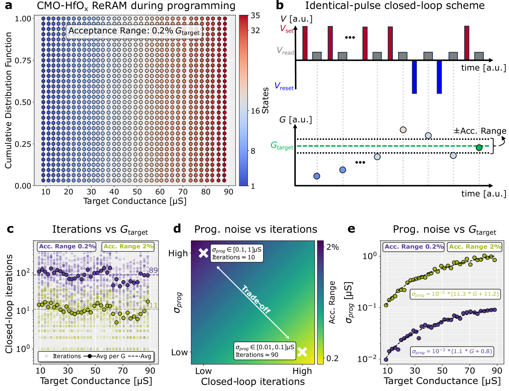
In memristor-based AIMC inference accelerators, pre-trained normalized weights are initially mapped into target conductances and subsequently programmed into hardware in an iterative process known as weight transfer. This iterative process, which stops once the programmed conductance converges to the target value within a defined acceptance range, inherently introduces an error due to the analog nature of conductance weights. This error, described by a normal distribution with the standard deviation referred to as programming noise ( $\sigma_{\rm prog}$ ), leads to a drop in MVM accuracy. To quantify this non-ideality, the non-volatile multi-level capability of the CMO/HfO x ReRAM array is characterized. Fig. 3 a shows the experimental cumulative distribution of conductance values for 35 representative levels, with all states sharply separated and without any overlap. Fig. 3 b shows a schematic representation of the closed-loop (i.e., program-verify) scheme, where identical set and reset pulse trains are employed to program each ReRAM cell to its target conductance within a desired acceptance range (see ”Methods” section ”Identical-pulse closed-loop scheme” for details). Selecting programming conditions involves a fundamental trade-off: a narrower acceptance range can improve programming precision by reducing programming noise, but it increases the number of iterations required for convergence (see Fig. 3 d). Besides the longer programming time, other non-idealities to consider when choosing the acceptance range are (1) the conductance relaxation immediately after programming, which is characterized in 2.2.2 for CMO/HfO x ReRAM devices, and (2) read noise, which has already been characterized between 0.2% and 2% of G target for CMO/HfO x ReRAM devices [25] within a similar conductance range used in this work. The trade-off between the programming noise and the number of iterations is characterized for two representative acceptance range intervals: 0.2% and 2% of G target, respectively. Fig. 3 c illustrates the experimental number of pulses needed to converge to the G target using the two representative acceptance ranges. On average, each cell requires approximately 11 and 89 set / reset pulses for acceptance ranges of 2% and 0.2% of G target, respectively. Since the acceptance range is defined as a percentage of G target, the number of iterations required for convergence is almost independent of the target conductance value. In the Supplementary Information, Fig. S5 a shows the experimental cumulative distribution of conductance values for the same 35 representative levels presented in Fig. 3 a, but using 2% G target as acceptance range. The standard deviation of the representative conductance levels is extracted and fitted as a linear function of the target conductance (dashed lines), as shown in Fig. 3 e, for both acceptance ranges. For all conductance levels, a standard deviation of less than 0.1 µS (1 µS) is achieved considering 0.2% G target (2% G target) as the acceptance range. This is more than one order of magnitude lower compared to other memristive technologies, such as phase-change memory (PCM) arrays, targeting similar conductance ranges [34, 35, 36]. These results demonstrate that CMO/HfO x ReRAM cells achieve an almost ideal weight transfer during programming, enabling the distinction of more than 32 states (5 bits).
<details>
<summary>x3.png Details</summary>
### Visual Description
## Chart/Diagram Type: Multi-Panel Figure: Programming of ReRAM
### Overview
The image presents a multi-panel figure (a-e) illustrating the programming of a CMO-HfOₓ ReRAM (Resistive Random-Access Memory) using a closed-loop scheme. The figure explores the relationship between target conductance, programming noise, and the number of iterations required for programming.
### Components/Axes
**Panel a: Cumulative Distribution Function vs. Target Conductance**
* **Title:** CMO-HfOₓ ReRAM during programming
* **Axes:**
* X-axis: Target Conductance [µS], ranging from 10 to 90 in increments of 10.
* Y-axis: Cumulative Distribution Function, ranging from 0.00 to 1.00 in increments of 0.25.
* **Color Scale:** A color gradient from blue to red, representing the number of states, ranging from 1 to 35.
* **Annotation:** "Acceptance Range: 0.2% Gtarget"
**Panel b: Identical-pulse closed-loop scheme**
* **Title:** Identical-pulse closed-loop scheme
* **Top Subplot Axes:**
* Y-axis: V [a.u.] (Arbitrary Units)
* Annotations: Vset (red), Vread (gray), Vreset (blue)
* X-axis: time [a.u.] (Arbitrary Units)
* **Bottom Subplot Axes:**
* Y-axis: G [a.u.] (Arbitrary Units)
* Annotation: Gtarget (green, dashed line)
* X-axis: time [a.u.] (Arbitrary Units)
* Annotation: ±Acc. Range (green bracket)
**Panel c: Iterations vs Gtarget**
* **Title:** Iterations vs Gtarget
* **Axes:**
* X-axis: Target Conductance [µS], ranging from 10 to 90 in increments of 20.
* Y-axis: Closed-loop iterations (logarithmic scale), ranging from 10⁰ to 10².
* **Data Series:**
* Iterations (gray dots)
* Avg per G (yellow dots)
* Avg (dashed lines):
* Acceptance Range 0.2% (purple, average around 89 iterations)
* Acceptance Range 2% (yellow, average around 11 iterations)
* **Annotations:** "Acc. Range 0.2%", "Acc. Range 2%"
**Panel d: Prog. noise vs iterations**
* **Title:** Prog. noise vs iterations
* **Axes:**
* X-axis: Closed-loop iterations (qualitative, Low to High)
* Y-axis: σprog (qualitative, Low to High)
* **Color Scale:** A color gradient from purple to yellow, representing the Acceptance Range, ranging from 0.2% to 2%.
* **Annotations:**
* "Trade-off" (white arrow)
* "σprog ∈ [0.1, 1] µS, Iterations ≈ 10" (white cross at top-left)
* "σprog ∈ [0.01, 0.1] µS, Iterations ≈ 90" (white cross at bottom-right)
**Panel e: Prog. noise vs Gtarget**
* **Title:** Prog. noise vs Gtarget
* **Axes:**
* X-axis: Target Conductance [µS], ranging from 10 to 90 in increments of 20.
* Y-axis: σprog [µS] (logarithmic scale), ranging from 10⁻² to 10⁰.
* **Data Series:**
* Acceptance Range 0.2% (purple dots): σprog = 10⁻³ * (1.1 * G + 0.8)
* Acceptance Range 2% (yellow dots): σprog = 10⁻³ * (11.3 * G + 11.2)
* **Annotations:** "Acc. Range 0.2%", "Acc. Range 2%"
### Detailed Analysis
**Panel a:** The cumulative distribution function shows how the states are distributed across different target conductance values. The color gradient indicates the density of states, with blue representing lower states and red representing higher states. The distribution shifts towards higher conductance values as the target conductance increases.
**Panel b:** This panel illustrates the identical-pulse closed-loop scheme. The top subplot shows the voltage pulses applied (Vset, Vread, Vreset) over time. The bottom subplot shows the resulting conductance (G) over time, converging towards the target conductance (Gtarget) within an acceptable range (±Acc. Range).
**Panel c:** This graph shows the relationship between the number of closed-loop iterations and the target conductance. The gray dots represent individual iterations, while the yellow dots represent the average number of iterations for each target conductance. The dashed lines indicate the average number of iterations for acceptance ranges of 0.2% (purple, ~89 iterations) and 2% (yellow, ~11 iterations).
**Panel d:** This heatmap illustrates the trade-off between programming noise (σprog) and the number of closed-loop iterations. Lower noise requires more iterations, and vice versa. The color gradient represents the acceptance range, with purple indicating a tighter acceptance range (0.2%) and yellow indicating a wider acceptance range (2%).
**Panel e:** This graph shows the relationship between programming noise (σprog) and target conductance. The purple dots represent an acceptance range of 0.2%, and the yellow dots represent an acceptance range of 2%. The equations provided describe the relationship between σprog and G for each acceptance range.
### Key Observations
* **Panel a:** The distribution of states shifts towards higher conductance values as the target conductance increases.
* **Panel b:** The closed-loop scheme converges towards the target conductance over time.
* **Panel c:** A tighter acceptance range (0.2%) requires significantly more iterations than a wider acceptance range (2%).
* **Panel d:** There is a clear trade-off between programming noise and the number of iterations.
* **Panel e:** Programming noise increases with target conductance for both acceptance ranges.
### Interpretation
The data presented in this figure demonstrates the programming characteristics of a CMO-HfOₓ ReRAM using a closed-loop scheme. The key findings are:
1. **Trade-off between Accuracy and Speed:** A tighter acceptance range (higher accuracy) requires more programming iterations (slower programming).
2. **Programming Noise Increases with Target Conductance:** As the target conductance increases, the programming noise also increases, making it more challenging to achieve precise programming at higher conductance levels.
3. **Closed-Loop Scheme Effectiveness:** The closed-loop scheme effectively converges towards the target conductance, but the number of iterations required depends on the desired accuracy and the target conductance value.
The figure highlights the importance of carefully considering the trade-offs between accuracy, speed, and noise when programming ReRAM devices. The data can be used to optimize programming algorithms and device parameters to achieve the desired performance characteristics.
</details>
Figure 3: Weight transfer characterization. a Cumulative distributions of 35 conductance states obtained using an identical-pulse closed-loop scheme with a 0.2% G target acceptance range. For each distribution, the entire CMO/HfO x ReRAM array was programmed to the corresponding G target, and the conductance values measured during the final closed-loop iteration (during programming) is reported. Each dot represents a 1T1R cell. b An example sequence of the identical-pulse closed-loop programming scheme utilized in this work. c Experimental number of closed-loop iterations as a function of G target for the two representative acceptance ranges. Each semitransparent point represents a 1T1R cell, the opaque points represent the average number of iterations per G target, and the horizontal dashed line indicates the overall average of the opaque points. d Graphical representation of the trade-off between programming noise and the number of iterations required for convergence, as a function of the acceptance range. e Experimental programming noise as a function of G target for the two representative acceptance ranges. Each point represents the standard deviation of the normal distribution measured across the entire array. The dashed lines in black indicate the corresponding linear fits.
2.2.2 Conductance relaxation and matrix-vector multiplication accuracy
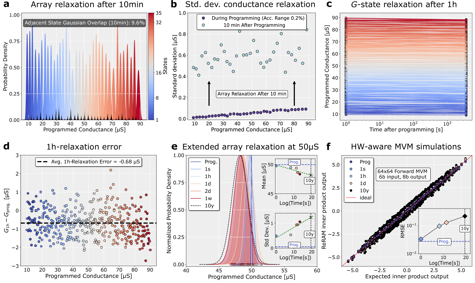
In addition to the excellent weight transfer accuracy during programming as presented in the previous section, the characterization of temporal conductance relaxation is critical to estimate the MVM accuracy over time. In analog ReRAM devices, a significant conductance relaxation has been observed immediately after programming (within 1 second) [9]. Following this initial abrupt conductance change, the relaxation process slows considerably [37, 9]. The physical cause of retention degradation is attributed to the Brownian motion of defects in the resistive switching layer [37]. In this section, the conductance relaxation of the CMO/HfO x ReRAM array after programming is characterized. Fig. 4 a shows the relaxation of the distributions previously reported in Fig. 3 a, approximately 10 minutes after programming. The 35 levels remain distinguishable 10 minutes after programming, with an average overlap of 9.6% between adjacent states gaussians, while the average standard deviation of the distributions increases to 0.6 µS, showing almost independence from the G target (see Fig. 4 b). The stability of the CMO/HfO x ReRAM conductance states is further assessed on a longer time-scale, up to 1 hour. To achieve so, a linearly spaced G target vector within the experimental conductance range of 10 µS to 90 µS is defined, with a fine step of 0.2 µS (400 points). Each G target value is programmed into a single ReRAM device within the array. Due to the size mismatch between the array (32 devices) and the G target vector (size 400), multiple measurement batches are needed. Fig. 4 c shows the experimental relaxation of the 400 programmed states within the entire conductance window, 1 second and 1 hour after programming, executed with the closed-loop scheme (see ”Methods” section ”Identical-pulse closed-loop scheme” for details) and with a 0.2% G target acceptance range. The exhibited conductance error induced by the relaxation process after 1 hour, computed as $G_{\mathrm{1h}}-G_{\mathrm{prog.}}$ , is plotted as a function of the programmed conductances in Fig. 4 d. After 1 hour, although both positive and negative relaxation errors are recorded, an average decrease in conductance is observed across all programmed states, with a relaxation error averaging around -0.7 µS. This highlights that the relaxation process in CMO/HfO x ReRAM devices leads, on average, to a decrease in the mean and an increase in the standard deviation of the Gaussian distributions regardless of the initial conductance state. Since the absolute magnitudes of the mean decrease and the standard deviation increase are independent of G target, an extended characterization of the relaxation process up to 1 week is conducted for a representative conductance state (50 µS). To achieve this, the array’s CMO/HfO x ReRAM devices are programmed using the identical-pulse closed-loop scheme to G target of 50 µS, with a 0.2% G target acceptance range. Fig. 4 e illustrates the experimental array relaxation over 1 week. The insets display the evolution of both the mean and standard deviation as a function of the logarithm of time after programming (in seconds), using a linear fit to predict the conductance distribution over a 10-year period. To assess the accuracy of analog MVM, a comprehensive set of non-idealities—both intrinsic to CMO/HfO x ReRAM devices and at the architecture level—is considered, including finite programming resolution with 0.2% G target acceptance range, conductance relaxation, limited ADC and DAC quantization, and IR-drop across array wires. Fig. 4 f shows the hardware-aware simulation results of the analog MVM using CMO/HfO x ReRAM cells, projected for up to 10 years from programming, compared to the expected floating-point (FP) result. The results are generated using a single 64×64 normally distributed random weight matrix and 100 normally distributed input vectors within the range [-1, 1] (see ”Methods” section ”HW-aware simulation of analog MVM” for details). Considering the input and output quantization of 6-bit and 8-bit respectively, the inset illustrates the time evolution of the root-mean-square error (RMSE) of the simulated analog MVM compared to the FP expected result. These results show that the CMO/HfO x ReRAM core enables accurate MVM operations, achieving an RMSE ranging from 0.03 at 1 second to 0.2 at 10 years after programming, compared to the ideal FP case. Fig. S6 in the Supplementary Information illustrates the impact of IR-drop and input/output quantization on the RMSE of an MVM performed on a 64×64 array. Over short time scales (within 1 hour), the primary accuracy bottleneck is the limited input/output quantization of 6-bit and 8-bit, respectively. Over longer periods, relaxation effects become the dominant source of non-ideality. In a larger 512×512 array, IR-drop emerges as the main accuracy bottleneck for analog MVM. Compared to the analog ReRAMs studied by Wan et al. [9], who report an experimentally determined RMSE of approximately 0.58 under conditions similar to those of this work, CMO/HfO x ReRAMs demonstrate a potential improvement in MVM accuracy by a factor of 20 and 3, 1 second and 10 years after programming, respectively. The excellent MVM accuracy results demonstrate the suitability of CMO/HfO x ReRAM devices for long-term AI inference applications, and lay the foundation for AI training acceleration, where short-term forward and backward MVMs are key steps.
<details>
<summary>x4.png Details</summary>
### Visual Description
## Multi-Chart: Array Relaxation and MVM Simulations
### Overview
The image presents a series of six charts (a-f) that analyze the relaxation behavior of a programmed array and its impact on hardware-aware Matrix-Vector Multiplication (MVM) simulations. The charts cover aspects like probability density of programmed conductance, standard deviation of conductance relaxation, G-state relaxation over time, relaxation error, extended array relaxation at a specific conductance, and the performance of MVM simulations.
### Components/Axes
**Chart a: Array relaxation after 10min**
* **Title:** Array relaxation after 10min
* **Y-axis:** Probability Density, Scale: 0.00 to 1.00, incremented by 0.25
* **X-axis:** Programmed Conductance [µS], Scale: 10 to 90, incremented by 10
* **Annotation:** Adjacent State Gaussian Overlap (10min): 9.6%
* **Color Gradient:** The bars are colored in a gradient from blue (left) to red (right), corresponding to lower and higher programmed conductance values.
* **States:** A secondary y-axis on the right side, ranging from 1 to 35.
**Chart b: Std. dev. conductance relaxation**
* **Title:** Std. dev. conductance relaxation
* **Y-axis:** Standard deviation [µS], Scale: 0.0 to 1.0, incremented by 0.2
* **X-axis:** Programmed Conductance [µS], Scale: 10 to 90, incremented by 10
* **Legend:**
* Blue-purple circles: During Programming (Acc. Range 0.2%)
* Light blue circles: 10 min After Programming
* **Annotation:** "Array Relaxation After 10 min" with arrows pointing to the respective data series.
**Chart c: G-state relaxation after 1h**
* **Title:** G-state relaxation after 1h
* **Y-axis:** Programmed Conductance [µS], Scale: 10 to 90, incremented by 10
* **X-axis:** Time after programming [s], Logarithmic scale from 10^0 to 10^3
* **Color Gradient:** The lines are colored in a gradient from blue (bottom) to red (top), corresponding to lower and higher programmed conductance values.
**Chart d: 1h-relaxation error**
* **Title:** 1h-relaxation error
* **Y-axis:** G1h - Gprog. [µS], Scale: -3 to 3, incremented by 1
* **X-axis:** Programmed Conductance [µS], Scale: 10 to 90, incremented by 10
* **Annotation:** Avg. 1h-Relaxation Error = -0.68 µS (dashed black line)
* **Color Gradient:** The data points are colored in a gradient from blue (left) to red (right), corresponding to lower and higher programmed conductance values.
**Chart e: Extended array relaxation at 50µS**
* **Title:** Extended array relaxation at 50µS
* **Main Plot:**
* **Y-axis:** Normalized Probability Density, Scale: 0.00 to 1.00, incremented by 0.25
* **X-axis:** Programmed Conductance [µS], Scale: 40 to 60, incremented by 5
* **Legend:**
* Dark Blue: Prog.
* Light Blue: 1s
* Orange: 1h
* Light Red: 1d
* Red: 2d
* Purple: 1w
* Dashed Black: 10y
* **Inset Plot 1 (top-right):**
* **Y-axis:** Mean [µS], Scale: 45 to 50, incremented by 5
* **X-axis:** Log(Time[s]), Scale: 0 to 20, incremented by 10
* **Data Points:** Prog, 1s, 1h, 1d, 10y
* **Inset Plot 2 (bottom-right):**
* **Y-axis:** Std Dev. [µS], Scale: 0 to 1, incremented by 1
* **X-axis:** Log(Time[s]), Scale: 0 to 20, incremented by 10
* **Data Points:** Prog, 1s, 1h, 1d, 10y
**Chart f: HW-aware MVM simulations**
* **Title:** HW-aware MVM simulations
* **Y-axis:** ReRAM inner product output
* **X-axis:** Expected inner product output
* **Legend:**
* Blue: Prog
* Light Blue: 1s
* Orange: 1h
* Light Red: 1d
* Black: 10y
* Red: ideal
* **Annotation:** 64x64 Forward MVM, 6b input, 8b output
* **Inset Plot:**
* **Y-axis:** RMSE
* **X-axis:** Log(Time[s]), Scale: 0 to 20, incremented by 10
* **Data Points:** Prog, 1s, 1h, 1d, 10y
### Detailed Analysis
**Chart a:** Shows the probability density of programmed conductance states after 10 minutes. The distribution appears multimodal, with peaks at various conductance levels. The color gradient indicates the programmed conductance value, with blue representing lower values and red representing higher values. The Adjacent State Gaussian Overlap is 9.6%, indicating the degree of overlap between adjacent conductance states.
**Chart b:** Illustrates the standard deviation of conductance relaxation. The "During Programming" data series shows very low standard deviation values, close to zero, across all programmed conductance levels. The "10 min After Programming" data series shows a higher standard deviation, fluctuating between approximately 0.4 and 0.8 µS.
**Chart c:** Depicts the G-state relaxation over time. Each line represents a different programmed conductance level, and the x-axis shows the time after programming on a logarithmic scale. The conductance values appear to decrease slightly over time, with the higher conductance states (red lines) showing a more pronounced decrease.
**Chart d:** Shows the 1-hour relaxation error (G1h - Gprog) as a function of programmed conductance. The data points are scattered around the zero line, with some points above and some below. The average 1-hour relaxation error is -0.68 µS, indicated by the dashed black line.
**Chart e:** Focuses on the extended array relaxation at 50 µS. The main plot shows the normalized probability density of the conductance at different time points (Prog, 1s, 1h, 1d, 2d, 1w, 10y). The inset plots show the mean and standard deviation of the conductance as a function of the logarithm of time. Both the mean and standard deviation decrease over time.
* **Main Plot:** The "Prog." (programmed) distribution is the narrowest, indicating the initial state. As time increases (1s, 1h, 1d, 2d, 1w), the distributions broaden, and the peak shifts slightly to the left. The "10y" (10 years) distribution is the broadest and most shifted.
* **Inset Plot 1 (Mean vs. Log(Time)):** The mean conductance decreases approximately linearly with the logarithm of time. The data points are:
* Prog: ~50 µS at Log(Time) = 0
* 1s: ~49.5 µS at Log(Time) ~ 0
* 1h: ~49 µS at Log(Time) ~ 3.6
* 1d: ~48.5 µS at Log(Time) ~ 4.6
* 10y: ~46 µS at Log(Time) ~ 8
* **Inset Plot 2 (Std Dev vs. Log(Time)):** The standard deviation also decreases approximately linearly with the logarithm of time.
* Prog: ~0.5 µS at Log(Time) = 0
* 1s: ~0.5 µS at Log(Time) ~ 0
* 1h: ~0.4 µS at Log(Time) ~ 3.6
* 1d: ~0.3 µS at Log(Time) ~ 4.6
* 10y: ~0.2 µS at Log(Time) ~ 8
**Chart f:** Presents the results of hardware-aware MVM simulations. The main plot shows the ReRAM inner product output versus the expected inner product output. The data points for different time points (Prog, 1s, 1h, 1d, 10y) are clustered closely around the "ideal" line, indicating good agreement between the ReRAM output and the expected output. The inset plot shows the Root Mean Square Error (RMSE) as a function of the logarithm of time. The RMSE increases over time, indicating a degradation in performance due to relaxation.
* **Main Plot:** The data points are tightly clustered around the ideal line, indicating high accuracy in the MVM operation.
* **Inset Plot (RMSE vs. Log(Time)):** The RMSE increases approximately linearly with the logarithm of time.
* Prog: ~0.01 at Log(Time) = 0
* 1s: ~0.01 at Log(Time) ~ 0
* 1h: ~0.02 at Log(Time) ~ 3.6
* 1d: ~0.03 at Log(Time) ~ 4.6
* 10y: ~0.1 at Log(Time) ~ 8
### Key Observations
* **Conductance Relaxation:** The programmed conductance values tend to decrease over time (Chart c and e).
* **Increased Variability:** The standard deviation of conductance increases shortly after programming (Chart b) but decreases over longer periods (Chart e).
* **Performance Degradation:** The accuracy of MVM simulations degrades over time due to conductance relaxation (Chart f).
* **Error Distribution:** The 1-hour relaxation error is centered around -0.68 µS (Chart d).
### Interpretation
The data suggests that conductance relaxation is a significant factor affecting the long-term stability and performance of ReRAM-based systems. While the initial programming accuracy is high, the conductance values drift over time, leading to increased variability and reduced accuracy in MVM operations. The extended array relaxation analysis at 50 µS (Chart e) provides insights into the temporal dynamics of this relaxation process, showing that both the mean and standard deviation of the conductance decrease over time. The hardware-aware MVM simulations (Chart f) demonstrate that this relaxation-induced drift can degrade the performance of neural network computations. The results highlight the need for strategies to mitigate the effects of conductance relaxation in ReRAM-based systems, such as periodic reprogramming or error correction techniques. The adjacent state Gaussian overlap of 9.6% indicates that the programmed states are relatively well-separated, but the relaxation process can cause these states to drift and potentially overlap, further degrading performance.
</details>
Figure 4: Conductance relaxation and MVM accuracy. a Probability density distributions of 35 conductance states approximately 10 minutes after programming. The black areas between adjacent Gaussian distributions represent the overlap of their tails. On average, an overlap of 9.6% is observed after 10 minutes. b The standard deviations of the 35 conductance states during programming (in purple) and 10 minutes after it (light blue). c Relaxation of 400 conductance states, with one device per G-state, measured 1 second and 1 hour after programming. d Relaxation error 1 hour after programming. A negative and nearly G-independent average error (dashed line) indicates that relaxation in CMO/HfO x ReRAMs tends toward a slight conductance decrease and is state-independent. e Experimental array relaxation of a representative 50 µS state, up to 1 week after programming with 0.2% G target acceptance range. Each probability density distribution is normalized to its maximum for graphical representation. The experimental data used to extract the distributions are represented as points aligned to the y=0 horizontal axis. Insets show the time dependence of the mean and standard deviation. Dashed blue lines represent the conditions during programming, once the convergence to G target is reached, while a linear fit (green dashed line) extrapolates the distribution 10 years after programming (dashed black line). f Analog MVM accuracy simulations using a 64x64 CMO/HfO x ReRAM array as a function of time after programming (indicated by different colors). The inset shows the expected RMSE compared to the ideal FP result. Experimental programming noise, conductance relaxation, limited input/output quantization and IR-drop are considered in this assessment.
2.3 Analog training with CMO/HfO x ReRAM core
To efficiently tackle deep learning workloads, the analog AI accelerator must not only perform forward and backward passes (MVMs), but most importantly, allow for weight updates [38]. During backpropagation, the synaptic weights are modified according to the gradient of the corresponding layer. Therefore, the device conductance must be gradually modified in both positive and negative directions to represent analog weight changes. Analog CMO/HfO x ReRAM arrays not only allow for bidirectional conductance updates, but additionally enable parallel weight updating by following a stochastic open-loop pulse scheme [20, 21]. Remarkably, the parallel and open-loop update scheme significantly accelerates training compared to serial and closed-loop methods, providing efficiency gains of several orders of magnitude and advantages in system design complexity [39]. In this section, the bidirectional open-loop response of the CMO/HfO x ReRAM array, required during Tiki-Taka training, is characterized. Specifically, the analog conductance potentiation, depression and symmetry point are measured. Subsequently, the devices’ responses are statistically reproduced in the open-source ’aihwkit’ simulation platform developed by IBM [38]. Finally, this hardware-aware device model, which includes device variabilities, is used to simulate the training of representative neural networks using the AGAD learning algorithm. This novel analog training algorithm relaxes the symmetry requirements of previous Tiki-Taka versions by incorporating additional digital computations on-the-fly [23].
2.3.1 Open-loop ReRAM array characterization
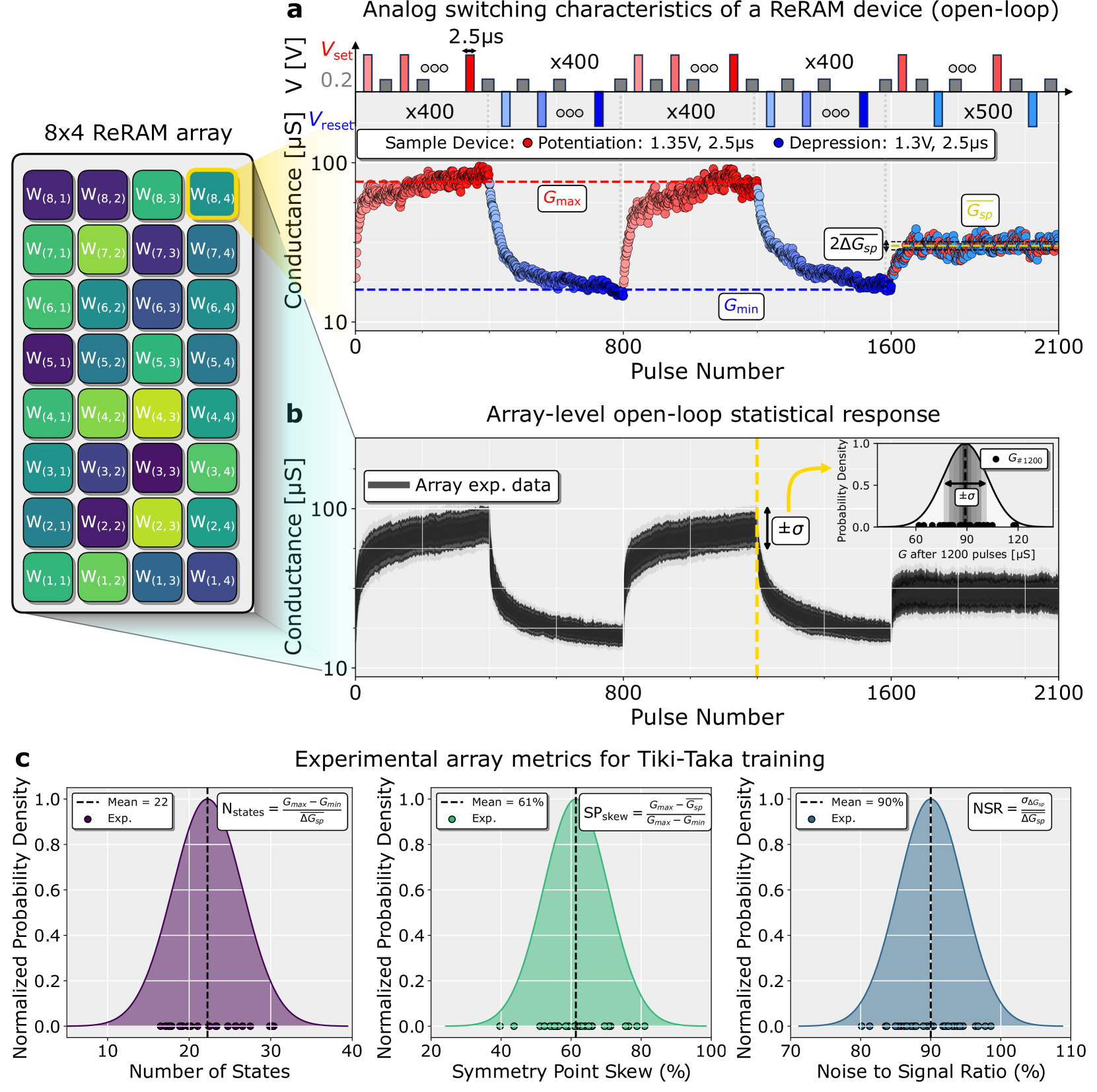
Fig. 5 a shows the experimental conductance change of a representative CMO/HfO x ReRAM device within the array upon applying identical-voltage pulse trains with alternating polarity in batches of 400. Subsequently, a sequence of 500 pulses with alternating polarity, consisting of 1-pulse-up followed by 1-pulse-down, is applied to experimentally determine the symmetry point. The same open-loop programming scheme, with $V_{\rm set}=1.35\,\mathrm{V}$ ( $V_{\rm G}=1.4\,\mathrm{V}$ ) and $V_{\rm reset}=-1.3\,\mathrm{V}$ ( $V_{\rm G}=3.3\,\mathrm{V}$ ), each lasting 2.5 µs, is applied to all devices in the 8x4 array. The set / reset pulse width is limited by the experimental setup, although previous work has demonstrated CMO/HfO x ReRAM switching with pulses as short as $60\,\mathrm{ns}$ [25]. Due to inter-device (device-to-device) and intra-device (cycle-to-cycle) variabilities, the experimental response of each device to a given number of identical pulses exhibits some level of variability (see Fig. S7 in the Supplementary Information). Therefore, for each pulse, a Gaussian distribution of the measured conductance states among the devices is extracted. For statistical relevance, Fig. 5 b shows the experimental standard deviation of the array response to the open-loop scheme as a function of the pulse number, represented in grey. To realistically assess the accuracy of analog training with CMO/HfO x ReRAM devices, the key figures of merit of the device training characterization—such as the number of states, the symmetry point skew, and the noise-to-signal ratio (NSR)—are first extracted from experimental data, as defined below.
$$
\displaystyle\mathrm{N}_{\rm states}=\frac{G_{\rm max}-G_{\rm min}}{\overline{%
\Delta G_{\rm sp}}} \tag{1}
$$
$$
\displaystyle\mathrm{SP}_{\rm skew}=\frac{G_{\rm max}-\overline{G_{\rm sp}}}{G%
_{\rm max}-G_{\rm min}} \tag{2}
$$
$$
\displaystyle\mathrm{NSR}=\frac{\sigma_{\Delta G_{\rm sp}}}{\overline{\Delta G%
_{\rm sp}}} \tag{3}
$$
$G_{\rm max}$ and $G_{\rm min}$ represent the maximum and minimum values extracted from the full conductance swings, while $\overline{G_{\rm sp}}$ , $\overline{\Delta G_{\rm sp}}$ and $\sigma_{\Delta G_{sp}}$ denote the values of the mean conductance, mean conductance update and standard deviation of the conductance update at the symmetry point during the 1-pulse-up, 1-pulse-down procedure, respectively. Fig. 5 c shows the experimental Gaussian distributions of these metrics for the 32 devices within the array. The results indicate an average of 22 states, with a range from 16 to 33. A shift in the $G_{\rm sp}$ (or SP skew) of 61% is measured, reflecting a negative trend in the device asymmetry where the down response is steeper than the up response. An average NSR of 90% among the devices is obtained, demonstrating the capability to discriminate between pulses up and down around the symmetry point. This parameter reflects the intrinsic noise on the device’s response under identical conditions, highlighting an intra-device variation [38]. Previous studies on similar CMO/HfO x ReRAM systems [24] extracted these metrics from isolated 1R devices using an optimized open-loop scheme tailored to each device. In contrast, this work demonstrates for the first time that a single open-loop identical pulse scheme enables reliable operation of the entire CMO/HfO x 1T1R array, ensuring consistent performance across the array.
<details>
<summary>x5.png Details</summary>
### Visual Description
## ReRAM Device Characteristics and Array Metrics
### Overview
The image presents data on the analog switching characteristics of a ReRAM (Resistive Random-Access Memory) device in an open-loop configuration. It includes plots showing conductance changes over pulse number, statistical response of an array, and experimental array metrics related to Tiki-Taka training.
### Components/Axes
**Panel a: Analog Switching Characteristics**
* **Title:** Analog switching characteristics of a ReRAM device (open-loop)
* **Y-axis:** Conductance [µS], with a logarithmic scale from 10 to 100.
* **X-axis:** Pulse Number, ranging from 0 to 2100.
* **Voltage Pulses:** A schematic at the top shows alternating positive (Vset) and negative (Vreset) voltage pulses. Vset pulses are shown in red, and Vreset pulses are shown in blue. The pulse width is 2.5µs.
* **Annotations:**
* "x400", "x500" indicate the number of pulses in each block.
* "Sample Device: Potentiation: 1.35V, 2.5µs; Depression: 1.3V, 2.5µs" describes the pulse parameters.
* **Data Series:**
* A red-to-blue gradient line shows the conductance of a sample device over time. The red portion represents potentiation, and the blue portion represents depression.
* **Horizontal Lines:**
* A red dashed line labeled "Gmax" is at approximately 90 µS.
* A blue dashed line labeled "Gmin" is at approximately 15 µS.
* A yellow line labeled "Gsp" is at approximately 40 µS.
* A yellow line labeled "2ΔGsp" is at approximately 40 µS.
**Panel b: Array-Level Open-Loop Statistical Response**
* **Title:** Array-level open-loop statistical response
* **Y-axis:** Conductance [µS], with a logarithmic scale from 10 to 100.
* **X-axis:** Pulse Number, ranging from 0 to 2100.
* **Data Series:**
* A gray shaded region represents the array experimental data.
* **Vertical Line:**
* A yellow dashed line is present at x = 1200.
* **Annotation:**
* "±σ" indicates the standard deviation around the conductance value at the yellow line.
* **Inset Plot:**
* **Title:** G after 1200 pulses [µS]
* **Y-axis:** Probability Density, ranging from 0.0 to 1.0.
* **X-axis:** G after 1200 pulses [µS], ranging from 60 to 120.
* A black curve represents the probability density of the conductance after 1200 pulses.
* A black dot labeled "G#1200" is at approximately 90 µS.
* "±σ" indicates the standard deviation around the mean conductance value.
**Panel c: Experimental Array Metrics for Tiki-Taka Training**
* **Title:** Experimental array metrics for Tiki-Taka training
* **Subplots (from left to right):**
* **Number of States:**
* **Y-axis:** Normalized Probability Density, ranging from 0.0 to 1.0.
* **X-axis:** Number of States, ranging from 10 to 40.
* A purple curve represents the probability density.
* A black dashed line indicates the mean at 22.
* "Nstates = (Gmax - Gmin) / ΔGsp" is the formula for the number of states.
* Black dots represent experimental data points.
* "Mean = 22"
* "Exp."
* **Symmetry Point Skew:**
* **Y-axis:** Normalized Probability Density, ranging from 0.0 to 1.0.
* **X-axis:** Symmetry Point Skew (%), ranging from 20 to 100.
* A green curve represents the probability density.
* A black dashed line indicates the mean at 61%.
* "SPskew = (Gmax - Gsp) / (Gmax - Gmin)" is the formula for the symmetry point skew.
* Green dots represent experimental data points.
* "Mean = 61%"
* "Exp."
* **Noise to Signal Ratio:**
* **Y-axis:** Normalized Probability Density, ranging from 0.0 to 1.0.
* **X-axis:** Noise to Signal Ratio (%), ranging from 70 to 110.
* A blue curve represents the probability density.
* A black dashed line indicates the mean at 90%.
* "NSR = σΔGsp / ΔGsp" is the formula for the noise-to-signal ratio.
* Blue dots represent experimental data points.
* "Mean = 90%"
* "Exp."
**8x4 ReRAM Array Diagram**
* A schematic of an 8x4 ReRAM array is shown on the left side of the image.
* Each cell is labeled as W(row, column), where row ranges from 1 to 8 and column ranges from 1 to 4.
* The cells are colored in shades of green and purple.
* The cell W(7,4) is highlighted with a yellow border.
### Detailed Analysis
**Panel a:**
* The conductance initially increases rapidly with the application of positive voltage pulses (potentiation), reaching a maximum value (Gmax) of approximately 90 µS.
* After approximately 400 pulses, the polarity is switched to negative voltage pulses (depression), and the conductance decreases rapidly, reaching a minimum value (Gmin) of approximately 15 µS.
* The conductance then fluctuates around an intermediate value (Gsp) of approximately 40 µS.
**Panel b:**
* The array-level data shows a similar trend to the single-device data, but with more variability, represented by the gray shaded region.
* The inset plot shows the distribution of conductance values after 1200 pulses, with a mean value around 90 µS and a standard deviation of ±σ.
**Panel c:**
* The number of states (Nstates) has a mean value of 22.
* The symmetry point skew (SPskew) has a mean value of 61%.
* The noise-to-signal ratio (NSR) has a mean value of 90%.
### Key Observations
* The ReRAM device exhibits analog switching behavior, with conductance values that can be continuously adjusted by applying voltage pulses.
* The array-level data shows more variability than the single-device data, indicating device-to-device variations.
* The experimental array metrics provide insights into the performance of the ReRAM array for Tiki-Taka training.
### Interpretation
The data suggests that the ReRAM device is capable of analog switching, which is essential for implementing neuromorphic computing architectures. The array-level data highlights the importance of considering device-to-device variations when designing ReRAM-based systems. The experimental array metrics provide a quantitative assessment of the ReRAM array's performance for Tiki-Taka training, which is a specific type of machine learning algorithm. The high noise-to-signal ratio (NSR) could be a limiting factor for the performance of the ReRAM array in certain applications.
</details>
Figure 5: Open-loop array characterization for on-chip training. a Bidirectional accumulative response and symmetry point of a representative device in the array. The top inset shows the open-loop identical pulse scheme used for the synaptic potentiation (red) and depression (blue). A conceptual illustration of the 8x4 CMO/HfO x ReRAM array is depicted on the left. b Array statistical open-loop response to identical pulses. The grey area represents the standard deviation of the experimental Gaussian distributions, each corresponding to a specific pulse number. The inset shows a representative example of the experimental G-distribution at pulse number 1200. The raw data can be found in Figure S9 of the Supporting Information. c The experimental probability densities of N states, SP skew and NSR, respectively. The experimental data used to extract the distributions are represented as points aligned along the y=0 horizontal axis.
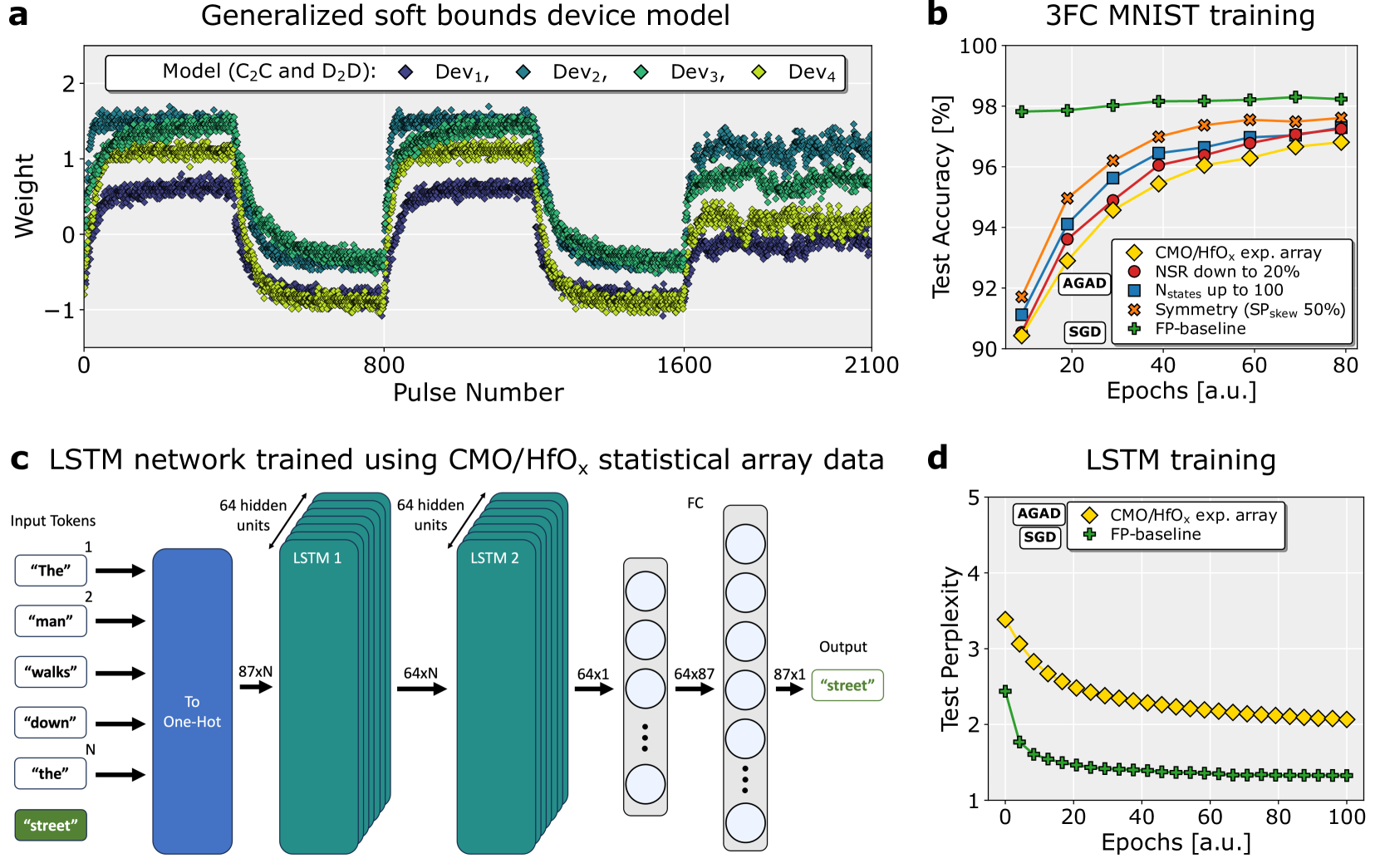
2.3.2 Tiki-Taka training simulations
To perform realistic hardware-aware training simulations, the experimental device response is reproduced on software using the generalized soft bounds model implemented in the ’aihwkit’ [40], which better captures the bidirectional resistive switching behavior (see Fig. S8 in Supplementary Information) and accounts for intra- and inter-device variabilities (see cycle-to-cycle and device-to-device variations in Fig. 6 a). Additionally, Gaussian distributions are modelled based on parameters extracted from device characterization ( $G_{\rm max}$ , $G_{\rm min}$ , $\Delta G_{\rm sp}$ , NSR, SP skew) to account for device-to-device variability observed in the experimental characterization (see ”Methods” section ”Intra and inter-device variability” for details). This Gaussian fitting approach allows defining various device presets—characterized by the same model but with different parameter settings—to represent the synapses across the neural network. A realistic simulation setup is obtained by exclusively considering experimentally obtained parameters to reproduce the device trace (see ”Methods” section ”Generalized soft bounds model” for details). The device model is defined based on the observed conductance window and number of states, without assuming asymptotic behavior for an infinite number of pulses. This prevents overestimation of both the conductance window and the number of states (material states), enhancing the fidelity of the simulation. To validate analog training with CMO/HfO x ReRAM technology, a 3-layer fully connected (FC) neural network was trained on the MNIST dataset for image classification. In addition, the impact of the device’s number of states, asymmetry, and noise-to-signal ratio on accuracy and convergence time is evaluated by simulating identical networks in which each property is individually enhanced, while keeping the others fixed at the experimentally derived values. Literature has shown that these device characteristics critically influence the convergence of analog training algorithms [23]. Therefore, this method assesses the deviation of the current CMO/HfO x ReRAM device properties from the ideal analog resistive device scenario. Moreover, to show the scalability of the CMO/HfO x ReRAM technology to more computationally-intensive tasks, such as time series processing, a 2-layer long short-term memory (LSTM) network was trained on War and Peace text sequences to predict the next token. Each network is initially trained using conventional stochastic gradient descent (SGD) based backpropagation with 32-bit FP precision, serving as the baseline performance. Fig. 6 b illustrates the accuracy per epoch for the FP-baseline trained with SGD (in green) and the analog network trained using AGAD, evaluated under four different parameter settings: (1) properties extracted from the experimental array (in yellow), (2) reduced NSR to 20% (in red), (3) average of N states = 100 states (in blue), and (4) zero average device asymmetry (in orange). Using symmetrical device presets, i.e. with an average SP skew of 50%, improves accuracy by 0.7% with respect to analog training with CMO/HfO x ReRAM experimentally derived configuration (96.9%), landing an accuracy of 97.6%, a 0.7% lower than the FP-SGD baseline (98.3%). The other two configurations show less performance improvement, indicating more resilience of the AGAD-training to device’s N states and NSR. Additionally, a 2-layer LSTM network with 64 memory states each (see Fig. 6 c), is trained with the experimentally obtained configuration. The performance is measured using the exponential of the cross-entropy loss, i.e. the test perplexity metric, which quantifies the certainty of the token prediction. Results in Fig. 6 d demonstrate the capabilities of the CMO/HfO x ReRAM technology on more complex network architectures, such as LSTMs, and computationally demanding tasks, exhibiting performance comparable to the FP-equivalent, with an approximate 0.7% difference in test perplexity.
<details>
<summary>x6.png Details</summary>
### Visual Description
## Chart/Diagram Type: Composite Figure
### Overview
The image presents a composite figure comprising four sub-figures (a, b, c, and d) that relate to device modeling, neural network training, and performance evaluation. Sub-figure (a) displays the weight changes of different devices over pulse numbers. Sub-figure (b) shows the test accuracy of a 3FC MNIST training model over epochs. Sub-figure (c) illustrates an LSTM network trained using CMO/HfOx statistical array data. Sub-figure (d) presents the test perplexity of LSTM training over epochs.
### Components/Axes
**Sub-figure a: Generalized soft bounds device model**
* **Title:** Generalized soft bounds device model
* **X-axis:** Pulse Number, ranging from 0 to 2100. Axis markers are present at 0, 800, 1600, and 2100.
* **Y-axis:** Weight, ranging from -1 to 2. Axis markers are present at -1, 0, 1, and 2.
* **Legend (top-center):** Model (C2C and D2D):
* Dev1 (dark blue diamonds)
* Dev2 (dark green diamonds)
* Dev3 (light green diamonds)
* Dev4 (yellow-green diamonds)
**Sub-figure b: 3FC MNIST training**
* **Title:** 3FC MNIST training
* **X-axis:** Epochs [a.u.], ranging from 20 to 80. Axis markers are present at 20, 40, 60, and 80.
* **Y-axis:** Test Accuracy [%], ranging from 90 to 100. Axis markers are present at 90, 92, 94, 96, 98, and 100.
* **Legend (right-center):**
* CMO/HfOx exp. array (yellow diamonds)
* NSR down to 20% (red circles)
* Nstates up to 100 (blue squares)
* Symmetry (SPskew 50%) (brown crosses)
* FP-baseline (green plus signs)
* AGAD (no marker specified, inferred from plot)
* SGD (no marker specified, inferred from plot)
**Sub-figure c: LSTM network trained using CMO/HfOx statistical array data**
* **Title:** LSTM network trained using CMO/HfOx statistical array data
* **Components:**
* Input Tokens (left): "The", "man", "walks", "down", "the", "street"
* To One-Hot (left-center)
* LSTM 1: 64 hidden units, 87xN
* LSTM 2: 64 hidden units, 64xN
* FC (Fully Connected Layer) (right-center)
* Output (right): "street", 87x1, 64x87, 64x1
**Sub-figure d: LSTM training**
* **Title:** LSTM training
* **X-axis:** Epochs [a.u.], ranging from 0 to 100. Axis markers are present at 0, 20, 40, 60, 80, and 100.
* **Y-axis:** Test Perplexity, ranging from 1 to 5. Axis markers are present at 1, 2, 3, 4, and 5.
* **Legend (top-left):**
* CMO/HfOx exp. array (yellow diamonds)
* FP-baseline (green plus signs)
* AGAD (no marker specified, inferred from plot)
* SGD (no marker specified, inferred from plot)
### Detailed Analysis
**Sub-figure a: Generalized soft bounds device model**
* **Dev1 (dark blue diamonds):** Starts around 0.25, decreases to -0.75 around pulse number 800, then increases back to approximately 0.25 around pulse number 1600, and remains stable.
* **Dev2 (dark green diamonds):** Starts around 1.25, decreases to -0.25 around pulse number 800, then increases back to approximately 1.25 around pulse number 1600, and remains stable.
* **Dev3 (light green diamonds):** Starts around 1.5, decreases to -0.5 around pulse number 800, then increases back to approximately 1.5 around pulse number 1600, and remains stable.
* **Dev4 (yellow-green diamonds):** Starts around 1.75, decreases to -0.75 around pulse number 800, then increases back to approximately 1.75 around pulse number 1600, and remains stable.
**Sub-figure b: 3FC MNIST training**
* **CMO/HfOx exp. array (yellow diamonds):** Starts at approximately 90% accuracy at 20 epochs, increases to approximately 97% accuracy by 80 epochs.
* **NSR down to 20% (red circles):** Starts at approximately 92% accuracy at 20 epochs, increases to approximately 97.5% accuracy by 80 epochs.
* **Nstates up to 100 (blue squares):** Starts at approximately 93% accuracy at 20 epochs, increases to approximately 97% accuracy by 80 epochs.
* **Symmetry (SPskew 50%) (brown crosses):** Starts at approximately 91.5% accuracy at 20 epochs, increases to approximately 97.5% accuracy by 80 epochs.
* **FP-baseline (green plus signs):** Remains relatively stable at approximately 98% accuracy across all epochs.
**Sub-figure d: LSTM training**
* **CMO/HfOx exp. array (yellow diamonds):** Starts at approximately 3.5 perplexity at 0 epochs, decreases to approximately 2 perplexity by 100 epochs.
* **FP-baseline (green plus signs):** Starts at approximately 2.5 perplexity at 0 epochs, decreases to approximately 1.3 perplexity by 100 epochs.
### Key Observations
* In sub-figure (a), all four devices show a similar trend: a decrease in weight followed by an increase, suggesting a write-erase-write cycle.
* In sub-figure (b), the FP-baseline consistently outperforms the other training methods in terms of test accuracy.
* In sub-figure (d), the FP-baseline achieves lower test perplexity compared to the CMO/HfOx exp. array, indicating better performance.
### Interpretation
The data presented suggests that the FP-baseline method is more effective for both MNIST training (higher accuracy) and LSTM training (lower perplexity) compared to the other methods tested. The device model in sub-figure (a) demonstrates the ability of the devices to switch between states, which is crucial for memory applications. The LSTM network diagram in sub-figure (c) provides a visual representation of the network architecture used for the LSTM training. The combination of these sub-figures provides a comprehensive overview of the device characteristics, network architecture, and training performance.
</details>
Figure 6: Device model and on-chip training simulations. a Device presets generated using the generalized soft bounds model with experimentally extracted parameters of CMO/HfO x devices, including inter- and intra-device variabilities. b Training simulations of a 3-layer fully-connected neural network on MNIST (235K parameters), using 32-bit FP precision trained on SGD (in green). Analog training simulations were performed using AGAD considering the empirical distribution of the parameters (in yellow), enhanced NSR (in red), increased N states (in blue), and symmetrical device configurations (in orange). c LSTM network architecture for text forecasting on the War and Peace dataset (79K parameters). The architecture considers a sequence length of 100 tokens and accounts for 2 layers with 64 hidden units. d Training results of the FP baseline (in green) and the analog training with AGAD on the experimental device configuration (in yellow). The training setup can be found in the Supporting Information.
3 Discussion
An all-in-one technology platform based on analog filamentary CMO/HfO x ReRAM devices is presented. This platform addresses critical challenges in modern digital AI accelerators by overcoming the physical separation between memory and compute units. It enables the execution of forward and backward MVMs, along with weight updates and gradient computations, directly on a unified analog in-memory platform with $O(1)$ time complexity. This all-in-one approach fundamentally differs from DNN inference-only [9] and training-only [24, 41] analog accelerators. In inference-only accelerators, DNN weights are trained in software (i.e., off-chip) using traditional digital CPUs or GPUs and then programmed once onto the analog AI hardware accelerator. In training-only accelerators, the long-term retention capabilities and overall MVM accuracy for large array tiles are not assessed. In this work, a novel all-in-one analog computing platform, capable of both on-chip training and inference acceleration, is unveiled. The CMO/HfO x ReRAM devices are integrated in the BEOL of a NMOS transistor platform in a scalable 1T1R array architecture. The highly reproducible forming step demonstrates compatibility with NMOS rated for $\mathrm{3.3\,V}$ operation, while the uniform quasi-static 8W-cycling characteristics, achieved with voltage amplitudes of less than $±$ $\mathrm{1.5\,V}$ , exhibit a significant conductance window and a low off-state. The multi-bit capability of more than 32 states (5 bits), distinguishable after 10 minutes with less than 10% overlap error, is experimentally demonstrated using an identical-pulse closed-loop scheme. The characterization of the weight transfer reveals record-low programming noise ranging from $\mathrm{10\,nS}$ to $\mathrm{100\,nS}$ , more than one order of magnitude lower than that of other memristive technologies targeting similar conductance ranges [34, 35, 36]. Each conductance distribution exhibits a state-independent relaxation process over time, characterized by a slight shift of the mean toward lower conductance and an increase in the standard deviation. This independence of the relaxation process from the target conductance is advantageous for implementing effective compensation schemes in the future. Realistic MVM simulations on a 64x64 array tile, considering CMO/HfO x ReRAM device non-idealities such as finite weight transfer resolution, conductance relaxation, limited input/output quantization, and IR-drop across array wires, show an RMSE as low as 0.2 compared to the ideal FP-case, even 10 years after programming. This demonstrates that the CMO/HfO x ReRAM devices improve analog MVM accuracy by a factor of 20 and 3 compared to the state of the art [9], 1 second and 10 years after programming, respectively. Although this study was performed at room temperature, previous characterization of a similar CMO/HfO x ReRAM stack demonstrated the thermal stability of the analog states at high temperature (less than 4% drift after 72 hours at 85 °C) [24]. Future studies will focus on incorporating the experimental read noise of CMO/HfO x ReRAM devices, characterized between 0.2% and 2% of G target within a similar conductance range as used in this work [25], into MVM accuracy simulations. Although read noise is not included in the MVM simulations of this study, no significant additional drop in MVM accuracy is anticipated. In fact, the magnitude of read noise is much smaller than that of the relaxation process and of the effect of reduced input/output quantization, which dominate the RMSE on different timescales. Furthermore, simulation results demonstrate the suitability of CMO/HfO x ReRAM technology for large 512x512 array, with the IR-drop expected to become the primary accuracy bottleneck in this case. Finally, the electrical response of the CMO/HfO x ReRAM array to an open-loop scheme with identical pulses demonstrates the viability of this technology for on-chip training applications. A realistic device model, accounting for both inter- and intra-device variability, is derived from experimental data. Table 1 benchmarks the representative device model used in this work on the MNIST dataset against other approaches, highlighting its high fidelity in reproducing experimental device responses.
Table 1: Device model benchmarking: from simplified approaches to realistic non-ideality modeling
| Ti/HfO x [41] | Not-included | exp. states Measured number of analog states during open-loop device characterization. | BEOL array | TTv2 | Medium | 90.5 % |
| --- | --- | --- | --- | --- | --- | --- |
| Ta/TaO x [41] | Not-included | exp. states Measured number of analog states during open-loop device characterization. | BEOL array | TTv2 | Medium | 96.4 % |
| TaO x /HfO x [24] | included | material states The asymptotic number of states under an infinite number of pulses. | Single ReRAMs | TTv2 | Medium | 97.4 % |
| CMO x /HfO x This work. | included | exp. states Measured number of analog states during open-loop device characterization. | BEOL array | AGAD | High | 96.9 % |
| \botrule | | | | | | |
The impact of the device’s number of states, asymmetry and noise-to-signal ratio on training accuracy using the AGAD algorithm on MNIST is evaluated. This analysis demonstrates that, with the current device’s experimental properties, AGAD analog training achieves 96.9% accuracy, comparable to the ideal FP-baseline of 98.3%. To further improve analog training performance and bring results closer to the software equivalent, the key metric to enhance in the device is the symmetry. Finally, the on-chip analog training capabilities of the CMO/HfO x ReRAM technology are demonstrated on a more complex 2-layer LSTM network, showing comparable performance to its floating-point equivalent. In conclusion, the novel CMO/HfO x ReRAM all-in-one technology platform presented in this work lays the foundation for efficient and versatile analog chips capable of combining both training and inference capabilities, enabling autonomous, energy-efficient, and adaptable AI systems.
4 Methods
4.1 Device fabrication
The CMO/HfO x ReRAM array is based on 1T1R unit cells. In this configuration, the bottom electrode of the ReRAM device is connected in series to the drain of an n-type metal–oxide–semiconductor (NMOS) selector transistor. The transistor blocks sneak paths and ensures current compliance during electro-forming and programming of the ReRAM device. The NMOS transistors, rated for $\mathrm{3.3\,V}$ operation, are fabricated using a standard $\mathrm{130\,nm}$ foundry process with copper BEOL interconnects. The ReRAM devices are integrated on metal-8 layer. To prevent the oxidation of the copper vias during the ReRAM stack deposition, the $\mathrm{70\,nm}$ thick silicon nitride (SiN x) passivation layer from the foundry is used as a protective layer. On top of that, a $\mathrm{20\,nm}$ thick titanium nitride (TiN) bottom electrode and a $\mathrm{4\,nm}$ thick hafnium oxide (HfO x) layers are deposited by Plasma-Enhanced Atomic Layer Deposition (PEALD) process at 300 °C, while maintaining vacuum conditions to avoid oxidation of the TiN layer. Subsequently, a stack of layers consisting of a $\mathrm{20\,nm}$ thick conductive metal-oxide (CMO), a $\mathrm{20\,nm}$ thick titanium nitride (TiN), and a $\mathrm{50\,nm}$ thick tungsten (W) is deposited by sputtering and patterned through a lithography step. A $\mathrm{100\,nm}$ thick silicon oxide (SiO x) layer is sputtered as passivation. The passivation layer is then patterned to expose the W top electrode and the copper via in the metal-8 layer beneath the bottom electrode. The ReRAM fabrication is completed using a titanium/gold lift-off process. In this approach, the TiN bottom electrode is connected to the metal-8 via through its vertical sidewalls using gold. The ReRAM BEOL patterning steps are performed through mask-based photolithography performed on a 6 $×$ 6 mm 2 die issued from a Multi Project Wafer (MPW). The area of the CMO/HfO x ReRAM devices presented in this work is 12 $×$ 12 µm 2. Previous studies on CMO/HfO x ReRAM devices have demonstrated scalability down to 200 $×$ 200 nm 2 [24, 26, 25]. Due to their filament-type nature, the performance of the ReRAM devices presented in this work is expected to remain similar for smaller areas.
4.2 ReRAM forming modelling
A 3D FEM of the CMO/HfO x ReRAM device, after the forming event, is used to simulate electronic transport by solving the continuity (4) and the Joule-heating (5) equations in steady state:
$$
\displaystyle\nabla\cdot J_{\rm e}=\nabla\cdot(\sigma(-\nabla V)=0 \tag{4}
$$
$$
\displaystyle\nabla\cdot(-k\nabla T)=J_{\rm e}\cdot E=Q_{\rm e} \tag{5}
$$
where $J_{\rm e}$ is the electric current density, $\sigma$ the electrical conductivity, $V$ the electric potential, $k$ the thermal conductivity and $Q_{\rm e}$ the heat source due to Joule heating. From the fit of the experimental array forming data in the low-voltage linear regime (from 0 to $0.2\,\mathrm{V}$ ), an average filament radius of $11\,\mathrm{nm}$ is extracted. The electrical and thermal conductivities of the materials in the ReRAM stack are taken from literature [26], by considering $\sigma_{\mathrm{CMO}}=5\,\mathrm{S/cm}$ and $k_{\mathrm{CMO}}=4\,\mathrm{W/mK}$ for the CMO layer used in this work. During the subsequent negative voltage sweep, the electrical conductivity of the CMO layer was used as a fitting parameter to model the radial redistribution of defects within the layer. Using experimental array data in the low-voltage linear regime (from 0 to $\mathrm{-0.2\,V}$ ), the resulting CMO electrical conductivity is $37\,\mathrm{S/cm}$ . Fig. S1 in Supplementary Information shows the results of the simulations.
4.3 ReRAM forming voltage extraction
The forming voltage of each 1T1R cell ( $V_{\mathrm{forming}}^{\mathrm{1T1R}}$ ) is defined as the voltage required to trigger the highest current increase ( $\max\left(\frac{dI}{dV}\right)$ ) during the quasi-static voltage sweep from 0 to $3.6\,\mathrm{V}$ (see Supplementary Information Fig. S2 a). The corresponding current is defined as the forming current ( $I_{\mathrm{forming}}^{\mathrm{1T1R}}$ ) (see Supplementary Information Fig. S2 b). Being the transistor driven by a constant $V_{\mathrm{G}}=1.2\,\mathrm{V}$ , it acts as a series resistor in the triode region before the forming event, when the ReRAM stack is highly insulating. After the forming event, when a conductive filament is created in the ReRAM device, the transistor ensures current compliance in the saturation region. The resistance of the transistor in the triode region at $V_{\mathrm{G}}=1.2\,\mathrm{V}$ is measured to be $R_{\mathrm{DS}}≈ 0.8\,\mathrm{k\Omega}$ (see Supplementary Information Fig. S2 c). Therefore, for each 1T1R cell, the actual ReRAM forming voltage is computed as $V_{\mathrm{forming}}^{\mathrm{ReRAM}}=V_{\mathrm{forming}}^{\mathrm{1T1R}}-R_{%
\mathrm{DS}}^{\mathrm{triode}}· I_{\mathrm{forming}}^{\mathrm{1T1R}}$ and reported in Fig. 2 c.
4.4 Analytical ReRAM transport modelling
In the 1T1R cell, the electronic current $I_{\rm e}$ is modelled as a trap-to-trap tunneling process within the CMO layer, as described in equation (6), following the model proposed by Mott and Gurney [42]. This model accounts for electron-hopping conduction across an energy barrier $\Delta E_{\rm e}$ , which remains uniform in all directions when there is no electric field applied. However, when an electric field is introduced, it modifies the energy barrier by $\mp$ $ea_{\rm e}E$ /2 for forward (backward) jumps, leading to a reduction (increase) in the barrier height.
$$
\displaystyle I_{\rm e}^{\rm Mott-Gurney}=2Aea_{\rm e}\nu_{\rm 0,e}N_{\rm e}%
\exp{(\frac{-\Delta E_{\rm e}}{k_{\rm B}T})}\sinh{(\frac{a_{\rm e}eE}{2k_{\rm B%
}T})} \tag{6}
$$
In equation (6), $e$ is the elementary charge, $k_{\rm B}$ is the Boltzmann’s constant, $a_{\rm e}$ is the hopping distance, $\nu_{\rm 0,e}$ is the electron attempt frequency, $N_{\rm e}$ is the density of electronic defect states in the sub-band of the CMO layer, $\Delta E_{\rm e}$ is the zero-field hopping energy barrier, $T$ and $E$ are the local temperature and electric field, respectively, and $A=\rm\pi\it r_{\rm CF}^{\rm 2}$ , $r_{\rm CF}$ being the filament radius, is the cross-sectional area of the filament at the interface with the CMO layer. The temperature and electric field in the CMO layer, for both LRS and HRS, are simulated by solving equations (4) and (5), while accounting for the experimental I-V non-linearity (see Supplementary Fig. S4 for details). The trap-to-trap tunneling parameters ( $N_{\rm e}$ , $\Delta E_{\rm e}$ , $a_{\rm e}$ ) are extracted from the fit using the same approach as described in previous works [26, 31].
4.5 Identical-pulse closed-loop scheme
The procedure begins with a quasi-static voltage sweep from 0 to $-1.5\,\mathrm{V}$ to reset each cell within the array to the HRS. Subsequently, a closed-loop scheme is initiated, which iteratively repeats the following two steps until convergence to G target within an acceptance range: (1) read the conductance of the ReRAM cell, and (2) if the measured value is below (above) the target conductance, apply a set (reset) programming pulse. During this iterative process, the cell conductance may fluctuate multiple times before eventually reaching the acceptance range. Starting from the HRS, this procedure is applied to the CMO/HfO x ReRAM array to sequentially program 35 representative conductance levels, ranging from approximately 10 µS to 90 µS, using acceptance ranges of both 0.2% G target and 2% G target. Unlike the conventional incremental-pulse closed-loop technique previously used for ReRAM [9, 43], where the amplitudes of set and reset pulses are gradually increased to achieve convergence, this work employs an identical-pulse closed-loop scheme to simplify the pulse generation circuitry design, using only two fixed amplitude values for the set ( $1.35\,\mathrm{V}$ or $1.5\,\mathrm{V}$ ) and two for the reset ( $-1.3\,\mathrm{V}$ or $-1.5\,\mathrm{V}$ ) pulses. Specifically, depending on G target, three ranges are used: from approximately 10 µS to 30 µS with $V_{\rm set}=1.35\,\mathrm{V}$ and $V_{\rm reset}=-1.5\,\mathrm{V}$ ; from 30 µS to 60 µS $V_{\rm set}=1.35\,\mathrm{V}$ and $V_{\rm reset}=-1.3\,\mathrm{V}$ ; and from 60 µS to 90 µS $V_{\rm set}=1.5\,\mathrm{V}$ and $V_{\rm reset}=-1.3\,\mathrm{V}$ . Fig. S5 b in Supplementary Information shows the flowchart of the identical-pulse closed-loop technique used in this work. The set / reset pulse width is fixed at 2.5 µs due to setup limitations, even though previous work has demonstrated CMO/HfO x ReRAM switching with pulse width as short as $60\,\mathrm{ns}$ [25]. The reading pulse amplitude and width are $V_{\rm read}=0.2\,\mathrm{V}$ and 300 µs, respectively. During the set, reset, and read operations of each 1T1R cell, the transistor’s gate voltage is controlled with constant values of $V_{\rm G}$ equal to $1.4\,\mathrm{V}$ , $3.3\,\mathrm{V}$ , and $3.3\,\mathrm{V}$ , respectively.
4.6 HW-aware simulation of analog MVM
The ’aihwkit’ [44] simulation tool was used to perform MVM assessments including non-ideal behaviors and noise, and their effect on the computation accuracy with respect to floating-point operations. The MVM simulation included the exhibited programming noise, conductance relaxation, input and output quantization, and IR-drop across array wires. The ’aihwkit’ allows to configure such noisy effects for dedicated memristive devices such as PCM by Nandakumar et al. [45] and ReRAM by Wan et al. [9]. Therefore, a unique phenomenological noise model for CMO/HfO x ReRAM devices for inference is developed to incorporate into the simulation both the characterized programming noise and conductance relaxation. Additionally, input and output are quantized with 6-bit and 8-bit resolution, respectively, and the IR-drop is considered, with 100 µS as the maximum ReRAM conductance level and a default segment wire resistance of 0.35 $\Omega$ .
4.6.1 Modelling the programming noise
For a target conductance G target, the device’s programmed conductance is defined as the target value plus normally distributed noise with a standard deviation $\sigma_{\rm prog}$ , which is a function of G target. As depicted in Fig. 3 e, the programming noise ( $\sigma_{\rm prog}$ ) of the CMO/HfO x ReRAM devices is statistically described by a first-order polynomial equation for a given acceptance range. The polynomial coefficients for acceptance ranges of 2% and 0.2% of G target are extracted from the characterization and introduced into the simulation environment. To assess the effects of the programming noise, each weight in the normalized matrix (ranging from [-1, 1]) is mapped to its corresponding conductance value (within the range [9, 89] µS from Fig. 3 a), and is then further adjusted by the programming noise described by the extracted linear functions. Therefore, the MVM accuracy can be assessed immediately after programming ( $t=0$ ), see Fig. 4 f.
4.6.2 Modelling the conductance relaxation
After programming, the conductance levels exhibit relaxation over time, as shown in Fig. 4. Unlike previous ReRAM drift characterizations reported by Wan et al. [9] the observed relaxation in CMO/HfO x ReRAM is approximately independent of the initial programmed conductance. Consequently, a new modelling approach in the ’aihwkit’ is needed to accurately simulate the conductance relaxation effect, which differs from the methods derived from previous literature on ReRAM [9]. The conductance relaxation mean and standard deviation are modelled independently of G target and solely as a function of time after programming. The coefficients of the first-order polynomials describing the time dependence of both the mean and standard deviation of the programmed conductance are incorporated into the simulation environment to estimate conductance variations at any given inference time. By doing so, the MVM accuracy can be estimated after a period of time up to 10 years.
4.7 HW-aware simulation of analog training
4.7.1 Generalized soft bounds model
The generalized soft bounds model (SBM) selection was based on the observed characteristics of the potentiation and depression since the devices did not strictly exhibit thorough saturation at the upper and lower boundaries (see Fig. S8 in Supplementary Information). The generalized SBM incorporates a tunable scale exponent ( $\gamma$ ) that describes abrupt and gradual trends toward the maximum and minimum conductance levels. This exponent parameter also varies depending on the conductance update direction. Therefore, the analytical expression of the generalized SBM implemented in the ’aihwkit’ includes an asymmetry factor ( $\gamma_{\rm up\_down}$ ) to account for this behavior [38]. However, these two parameters do not have a direct physical equivalence, and therefore, cannot be derived from experimental traces. Hereby, $\gamma$ and $\gamma_{\rm up\_down}$ are obtained for each device through an independent linear fitting of the generalized SBM to the experimental response. In addition to the analytical parameters of the generalized SBM, devices in the ’aihwkit’ are defined by a set of parameters that can be extracted from experimental traces. More precisely, the empirical maximum and minimum conductance, minimum conductance step size and its standard deviation, and the asymmetry between up and down response are considered ( $G_{\rm max}$ , $G_{\rm min}$ , $\Delta G_{\rm sp}$ , $\sigma_{\Delta G_{\rm sp}}$ , and $up\_down$ ). More details on the $up\_down$ parameter are provided in the Supplementary Information. In this regard, each simulated device is defined by 6 parameters: four empirically obtained ( $G_{\rm max}$ , $G_{\rm min}$ , $\Delta G_{\rm sp}$ and $up\_down$ ) and two analytically modelled from SBM linear fitting ( $\gamma$ and $\gamma_{\rm up\_down}$ ).
4.7.2 Intra and inter-device variability
By extracting the standard deviation of the minimum conductance step size ( $\sigma_{\Delta G_{\rm sp}}$ ) from the experimental traces and incorporating it into the simulation’s device model, the device response intrinsically includes noise from cycle to cycle. This provides a realistic device behavior with intra-device variability. Furthermore, the network devices shall include inter-device variabilities to perform physically accurate simulations. To achieve this, two multi-variate Gaussian distributions, G 1 and G 2, are created (see Fig. S9 in Supplementary Information). G 1 is extracted from the experimentally obtained parameters: N states (which accounts for variations across devices in the G-range and step) and SP in the normalized G-range, whereas G 2 is fitted to the analytical model parameters obtained from the fitted generalized SBM ( $\gamma$ and $\gamma_{\rm up\_down}$ ). Therefore, variables from G 1 showed statistical independence from those of G 2. New device instances are independently sampled from the two Gaussian distributions to represent synapses on the DNN layers. The instantiated CMO/HfO x ReRAM devices include variations in the device response, conductance ranges, and asymmetrical behavior, thus providing a more hardware-aware and realistic scenario for analog training simulation.
References
- \bibcommenthead
- Erdil [2024] Erdil, E.: Data Movement Bottlenecks to Large-Scale Model Training: Scaling Past 1e28 FLOP. Accessed: 2024-12-06 (2024). https://epoch.ai/blog/data-movement-bottlenecks-scaling-past-1e28-flop
- Jouppi et al. [2017] Jouppi, N.P., Young, C., Patil, N., Patterson, D., Agrawal, G., Bajwa, R., Bates, S., Bhatia, S., Boden, N., Borchers, A., Boyle, R., Cantin, P.-l., Chao, C., Clark, C., Coriell, J., Daley, M., Dau, M., Dean, J., Gelb, B., Ghaemmaghami, T.V., Gottipati, R., Gulland, W., Hagmann, R., Ho, C.R., Hogberg, D., Hu, J., Hundt, R., Hurt, D., Ibarz, J., Jaffey, A., Jaworski, A., Kaplan, A., Khaitan, H., Killebrew, D., Koch, A., Kumar, N., Lacy, S., Laudon, J., Law, J., Le, D., Leary, C., Liu, Z., Lucke, K., Lundin, A., MacKean, G., Maggiore, A., Mahony, M., Miller, K., Nagarajan, R., Narayanaswami, R., Ni, R., Nix, K., Norrie, T., Omernick, M., Penukonda, N., Phelps, A., Ross, J., Ross, M., Salek, A., Samadiani, E., Severn, C., Sizikov, G., Snelham, M., Souter, J., Steinberg, D., Swing, A., Tan, M., Thorson, G., Tian, B., Toma, H., Tuttle, E., Vasudevan, V., Walter, R., Wang, W., Wilcox, E., Yoon, D.H.: In-datacenter performance analysis of a tensor processing unit. ACM SIGARCH Computer Architecture News 45 (2017) https://doi.org/10.1145/3140659.3080246
- Sze et al. [2017] Sze, V., Chen, Y.H., Yang, T.J., Emer, J.S.: Efficient Processing of Deep Neural Networks: A Tutorial and Survey (2017). https://doi.org/10.1109/JPROC.2017.2761740
- Haensch et al. [2019] Haensch, W., Gokmen, T., Puri, R.: The next generation of deep learning hardware: Analog computing. Proceedings of the IEEE 107 (2019) https://doi.org/10.1109/JPROC.2018.2871057
- Sebastian et al. [2020] Sebastian, A., Le Gallo, M., Khaddam-Aljameh, R., Eleftheriou, E.: Memory devices and applications for in-memory computing (2020). https://doi.org/10.1038/s41565-020-0655-z
- Mutlu et al. [2019] Mutlu, O., Ghose, S., Gómez-Luna, J., Ausavarungnirun, R.: Processing data where it makes sense: Enabling in-memory computation. Microprocessors and Microsystems 67 (2019) https://doi.org/10.1016/j.micpro.2019.01.009
- Tsai et al. [2023] Tsai, H., Narayanan, P., Jain, S., Ambrogio, S., Hosokawa, K., Ishii, M., MacKin, C., Chen, C.T., Okazaki, A., Nomura, A., Boybat, I., Muralidhar, R., Frank, M.M., Yasuda, T., Friz, A., Kohda, Y., Chen, A., Fasoli, A., Rasch, M.J., Wozniak, S., Luquin, J., Narayanan, V., Burr, G.W.: Architectures and circuits for analog-memory-based hardware accelerators for deep neural networks (invited). In: Proceedings - IEEE International Symposium on Circuits and Systems, vol. 2023-May (2023). https://doi.org/10.1109/ISCAS46773.2023.10181650
- Burr et al. [2017] Burr, G.W., Shelby, R.M., Sebastian, A., Kim, S., Kim, S., Sidler, S., Virwani, K., Ishii, M., Narayanan, P., Fumarola, A., Sanches, L.L., Boybat, I., Le Gallo, M., Moon, K., Woo, J., Hwang, H., Leblebici, Y.: Neuromorphic computing using non-volatile memory (2017). https://doi.org/10.1080/23746149.2016.1259585
- Wan et al. [2022] Wan, W., Kubendran, R., Schaefer, C., Eryilmaz, S.B., Zhang, W., Wu, D., Deiss, S., Raina, P., Qian, H., Gao, B., Joshi, S., Wu, H., Wong, H.-S.P., Cauwenberghs, G.: A compute-in-memory chip based on resistive random-access memory. Nature 608 (7923), 504–512 (2022) https://doi.org/10.1038/s41586-022-04992-8
- Yao et al. [2020] Yao, P., Wu, H., Gao, B., Tang, J., Zhang, Q., Zhang, W., Yang, J.J., Qian, H.: Fully hardware-implemented memristor convolutional neural network. Nature 577 (2020) https://doi.org/10.1038/s41586-020-1942-4
- Ambrogio et al. [2023] Ambrogio, S., Narayanan, P., Okazaki, A., Fasoli, A., Mackin, C., Hosokawa, K., Nomura, A., Yasuda, T., Chen, A., Friz, A., Ishii, M., Luquin, J., Kohda, Y., Saulnier, N., Brew, K., Choi, S., Ok, I., Philip, T., Chan, V., Silvestre, C., Ahsan, I., Narayanan, V., Tsai, H., Burr, G.W.: An analog-ai chip for energy-efficient speech recognition and transcription. Nature 620 (2023) https://doi.org/10.1038/s41586-023-06337-5
- Le Gallo et al. [2023] Le Gallo, M., Khaddam-Aljameh, R., Stanisavljevic, M., Vasilopoulos, A., Kersting, B., Dazzi, M., Karunaratne, G., Brändli, M., Singh, A., Müller, S.M., Büchel, J., Timoneda, X., Joshi, V., Rasch, M.J., Egger, U., Garofalo, A., Petropoulos, A., Antonakopoulos, T., Brew, K., Choi, S., Ok, I., Philip, T., Chan, V., Silvestre, C., Ahsan, I., Saulnier, N., Narayanan, V., Francese, P.A., Eleftheriou, E., Sebastian, A.: A 64-core mixed-signal in-memory compute chip based on phase-change memory for deep neural network inference. Nature Electronics 6 (2023) https://doi.org/10.1038/s41928-023-01010-1
- [13] Gemini: A Family of Highly Capable Multimodal Models (2024). https://arxiv.org/abs/2312.11805
- Woo and Yu [2018] Woo, J., Yu, S.: Resistive memory-based analog synapse: The pursuit for linear and symmetric weight update. IEEE Nanotechnology Magazine 12 (2018) https://doi.org/10.1109/MNANO.2018.2844902
- Yin et al. [2020] Yin, S., Sun, X., Yu, S., Seo, J.S.: High-throughput in-memory computing for binary deep neural networks with monolithically integrated rram and 90-nm cmos. IEEE Transactions on Electron Devices 67 (2020) https://doi.org/10.1109/TED.2020.3015178
- Zahoor et al. [2020] Zahoor, F., Zulkifli, T.Z.A., Khanday, F.A.: Resistive Random Access Memory (RRAM): an Overview of Materials, Switching Mechanism, Performance, Multilevel Cell (mlc) Storage, Modeling, and Applications (2020). https://doi.org/10.1186/s11671-020-03299-9
- Tang et al. [2019] Tang, J., Bishop, D., Kim, S., Copel, M., Gokmen, T., Todorov, T., Shin, S., Lee, K.T., Solomon, P., Chan, K., Haensch, W., Rozen, J.: Ecram as scalable synaptic cell for high-speed, low-power neuromorphic computing. In: Technical Digest - International Electron Devices Meeting, IEDM, vol. 2018-December (2019). https://doi.org/10.1109/IEDM.2018.8614551
- Li et al. [2018] Li, Y., Kim, S., Sun, X., Solomon, P., Gokmen, T., Tsai, H., Koswatta, S., Ren, Z., Mo, R., Yeh, C.C., Haensch, W., Leobandung, E.: Capacitor-based cross-point array for analog neural network with record symmetry and linearity. In: Digest of Technical Papers - Symposium on VLSI Technology, vol. 2018-June (2018). https://doi.org/10.1109/VLSIT.2018.8510648
- Ielmini [2016] Ielmini, D.: Resistive switching memories based on metal oxides: Mechanisms, reliability and scaling (2016). https://doi.org/10.1088/0268-1242/31/6/063002
- Gokmen and Vlasov [2016] Gokmen, T., Vlasov, Y.: Acceleration of deep neural network training with resistive cross-point devices: Design considerations. Frontiers in Neuroscience 10 (2016) https://doi.org/10.3389/fnins.2016.00333
- Gokmen and Haensch [2020] Gokmen, T., Haensch, W.: Algorithm for training neural networks on resistive device arrays. Frontiers in Neuroscience 14 (2020) https://doi.org/10.3389/fnins.2020.00103
- Gong et al. [2022] Gong, N., Rasch, M.J., Seo, S.C., Gasasira, A., Solomon, P., Bragaglia, V., Consiglio, S., Higuchi, H., Park, C., Brew, K., Jamison, P., Catano, C., Saraf, I., Athena, F.F., Silvestre, C., Liu, X., Khan, B., Jain, N., McDermott, S., Johnson, R., Estrada-Raygoza, I., Li, J., Gokmen, T., Li, N., Pujari, R., Carta, F., Miyazoe, H., Frank, M.M., Koty, D., Yang, Q., Clark, R., Tapily, K., Wajda, C., Mosden, A., Shearer, J., Metz, A., Teehan, S., Saulnier, N., Offrein, B.J., Tsunomura, T., Leusink, G., Narayanan, V., Ando, T.: Deep learning acceleration in 14nm cmos compatible reram array: device, material and algorithm co-optimization. In: Technical Digest - International Electron Devices Meeting, IEDM, vol. 2022-December (2022). https://doi.org/10.1109/IEDM45625.2022.10019569
- Rasch et al. [2024] Rasch, M.J., Carta, F., Fagbohungbe, O., Gokmen, T.: Fast and robust analog in-memory deep neural network training. Nature Communications 15 (1), 7133 (2024) https://doi.org/10.1038/s41467-024-51221-z
- Stecconi et al. [2024] Stecconi, T., Bragaglia, V., Rasch, M.J., Carta, F., Horst, F., Falcone, D.F., Kate, S.C., Gong, N., Ando, T., Olziersky, A., Offrein, B.: Analog resistive switching devices for training deep neural networks with the novel tiki-taka algorithm. Nano Letters 24 (2024) https://doi.org/10.1021/acs.nanolett.3c03697
- Lombardo et al. [2024] Lombardo, D.G.F., Ram, M.S., Stecconi, T., Choi, W., La Porta, A., Falcone, D.F., Offrein, B., Bragaglia, V.: Read noise analysis in analog conductive-metal-oxide/hfox reram devices. In: 2024 Device Research Conference (DRC), pp. 1–2 (2024). https://doi.org/10.1109/DRC61706.2024.10643760
- Falcone et al. [2024] Falcone, D.F., Menzel, S., Stecconi, T., Galetta, M., La Porta, A., Offrein, B.J., Bragaglia, V.: Analytical modelling of the transport in analog filamentary conductive-metal-oxide/hfox reram devices. Nanoscale Horiz. 9, 775–784 (2024) https://doi.org/10.1039/D4NH00072B
- Padovani et al. [2015] Padovani, A., Larcher, L., Pirrotta, O., Vandelli, L., Bersuker, G.: Microscopic modeling of hfox rram operations: From forming to switching. IEEE Transactions on Electron Devices 62 (2015) https://doi.org/10.1109/TED.2015.2418114
- Kröger and Vink [1958] Kröger, F.A., Vink, H.J.: Relations between the concentrations of imperfections in solids. Journal of Physics and Chemistry of Solids 5 (1958) https://doi.org/10.1016/0022-3697(58)90069-6
- Padovani et al. [2012] Padovani, A., Larcher, L., Padovani, P., Cagli, C., Salvo, B.D.: Understanding the role of the ti metal electrode on the forming of hfo 2-based rrams. 2012 4th IEEE International Memory Workshop, IMW 2012, 1–4 (2012) https://doi.org/10.1109/IMW.2012.6213667
- Padovani et al. [2013] Padovani, A., Larcher, L., Bersuker, G., Pavan, P.: Charge transport and degradation in hfo2 and hfox dielectrics. IEEE Electron Device Letters 34, 680–82 (2013) https://doi.org/10.1109/LED.2013.2251602
- Falcone et al. [2023] Falcone, D.F., Menzel, S., Stecconi, T., La Porta, A., Carraria-Martinotti, L., Offrein, B.J., Bragaglia, V.: Physical modeling and design rules of analog conductive metal oxide-hfo2reram. In: 2023 IEEE International Memory Workshop, IMW 2023 - Proceedings (2023). https://doi.org/10.1109/IMW56887.2023.10145936
- Galetta et al. [2024] Galetta, M., Falcone, D.F., Menzel, S., La Porta, A., Stecconi, T., Choi, W., Offrein, B.J., Bragaglia, V.: Compact model of conductive-metal-oxide/hfox analog filamentary reram devices. In: 2024 IEEE European Solid-State Electronics Research Conference (ESSERC), pp. 749–752 (2024). https://doi.org/10.1109/ESSERC62670.2024.10719489
- Dittmann et al. [2021] Dittmann, R., Menzel, S., Waser, R.: Nanoionic memristive phenomena in metal oxides: the valence change mechanism. Advances in Physics 70 (2021) https://doi.org/10.1080/00018732.2022.2084006
- Joshi et al. [2020] Joshi, V., Le Gallo, M., Haefeli, S., Boybat, I., Nandakumar, S.R., Piveteau, C., Dazzi, M., Rajendran, B., Sebastian, A., Eleftheriou, E.: Accurate deep neural network inference using computational phase-change memory. Nature Communications 11 (2020) https://doi.org/10.1038/s41467-020-16108-9
- Tsai et al. [2019] Tsai, H., Ambrogio, S., MacKin, C., Narayanan, P., Shelby, R.M., Rocki, K., Chen, A., Burr, G.W.: Inference of long-short term memory networks at software-equivalent accuracy using 2.5m analog phase change memory devices. In: Digest of Technical Papers - Symposium on VLSI Technology, vol. 2019-June (2019). https://doi.org/10.23919/VLSIT.2019.8776519
- Le Gallo et al. [2018] Le Gallo, M., Sebastian, A., Cherubini, G., Giefers, H., Eleftheriou, E.: Compressed sensing with approximate message passing using in-memory computing. IEEE Transactions on Electron Devices 65 (2018) https://doi.org/%****␣main.bbl␣Line␣825␣****10.1109/TED.2018.2865352
- Zhao et al. [2018] Zhao, M., Wu, H., Gao, B., Zhang, Q., Wu, W., Wang, S., Xi, Y., Wu, D., Deng, N., Yu, S., Chen, H.Y., Qian, H.: Investigation of statistical retention of filamentary analog rram for neuromophic computing. In: Technical Digest - International Electron Devices Meeting, IEDM (2018). https://doi.org/10.1109/IEDM.2017.8268522
- Rasch et al. [2021] Rasch, M.J., Moreda, D., Gokmen, T., Le Gallo, M., Carta, F., Goldberg, C., El Maghraoui, K., Sebastian, A., Narayanan, V.: A flexible and fast pytorch toolkit for simulating training and inference on analog crossbar arrays. In: 2021 IEEE 3rd International Conference on Artificial Intelligence Circuits and Systems (AICAS), pp. 1–4 (2021). https://doi.org/10.1109/AICAS51828.2021.9458494
- Chen et al. [2023] Chen, P., Liu, F., Lin, P., Li, P., Xiao, Y., Zhang, B., Pan, G.: Open-loop analog programmable electrochemical memory array. Nature Communications 14 (2023) https://doi.org/10.1038/s41467-023-41958-4
- Frascaroli et al. [2018] Frascaroli, J., Brivio, S., Covi, E., Spiga, S.: Evidence of soft bound behaviour in analogue memristive devices for neuromorphic computing. Scientific Reports 8 (1), 7178 (2018) https://doi.org/10.1038/s41598-018-25376-x
- Abedin et al. [2023] Abedin, M., Gong, N., Beckmann, K., Liehr, M., Saraf, I., Straten, O.V., Ando, T., Cady, N.: Material to system-level benchmarking of cmos-integrated rram with ultra-fast switching for low power on-chip learning. Scientific Reports 13 (2023) https://doi.org/%****␣main.bbl␣Line␣925␣****10.1038/s41598-023-42214-x
- Mott and Gurney [1950] Mott, N.F., Gurney, R.W.: Electronic processes in ionic crystals. Oxford at the Clarendon Press, 2 ed. (1950)
- Alibart et al. [2012] Alibart, F., Gao, L., Hoskins, B.D., Strukov, D.B.: High precision tuning of state for memristive devices by adaptable variation-tolerant algorithm. Nanotechnology 23 (2012) https://doi.org/10.1088/0957-4484/23/7/075201
- Rasch et al. [2021] Rasch, M.J., Moreda, D., Gokmen, T., Le Gallo, M., Carta, F., Goldberg, C., El Maghraoui, K., Sebastian, A., Narayanan, V.: A flexible and fast pytorch toolkit for simulating training and inference on analog crossbar arrays. In: 2021 IEEE 3rd International Conference on Artificial Intelligence Circuits and Systems (AICAS), pp. 1–4 (2021). https://doi.org/10.1109/AICAS51828.2021.9458494
- Nandakumar et al. [2019] Nandakumar, S.R., Boybat, I., Joshi, V., Piveteau, C., Le Gallo, M., Rajendran, B., Sebastian, A., Eleftheriou, E.: Phase-change memory models for deep learning training and inference. In: 2019 26th IEEE International Conference on Electronics, Circuits and Systems (ICECS), pp. 727–730 (2019). https://doi.org/10.1109/ICECS46596.2019.8964852
\bmhead
Supplementary information This manuscript is supported by additional supplementary information provided in a separate document.
\bmhead
Acknowledgements The authors acknowledge the Binnig and Rohrer Nanotechnology Center (BRNC) at IBM Research Europe - Zurich. Special thanks go to Jean-Michel Portal, Eloi Muhr and Dominique Drouin for their contributions to the design of the NMOS transistors used in this work. The authors also extend their gratitude to Stephan Menzel for the fruitful discussions and to Ralph Heller for his assistance in wire-bonding the chip. This work is funded by SNSF ALMOND (grantID: 198612), by the European Union and Swiss state secretariat SERI within the H2020 MeM-Scales (grantID: 871371), MANIC (grantID: 861153), PHASTRAC (grantID: 101092096) and CHIST-ERA UNICO (20CH21-186952) projects.
\bmhead
Author contributions Conceptualization: D. F. F. and V. B.; hardware fabrication: D. F. F. and L. B. L.; electrical characterization: D. F. F, W. C., T. S., F. H., physical simulations: D. F. F.; inference and training simulations: V. C., D. F. F.; NMOS transistor design : N. G., F. A.; result interpretation: D. F. F., V. C., W. C., V. B., M. G., A. L. P. and B. J. O., supervision: V. B. and B. J. O.; manuscript writing: D. F. F., V. C.; data curation: D. F. F., V. C. and V. B.; manuscript review and editing: all authors; funding acquisition: B. J. O. and V. B.
\bmhead
Competing interests The authors declare no competing interests.
\bmhead
Data availability The data that support the plots within this paper and other findings of this study are available from the corresponding authors upon reasonable request.
\bmhead
Code availability The repositories containing the source codes used in this work for analog inference simulations and CMO/HfO x ReRAM noise model can be found at this link and this link, respectively.
Supplementary Information
<details>
<summary>x7.png Details</summary>
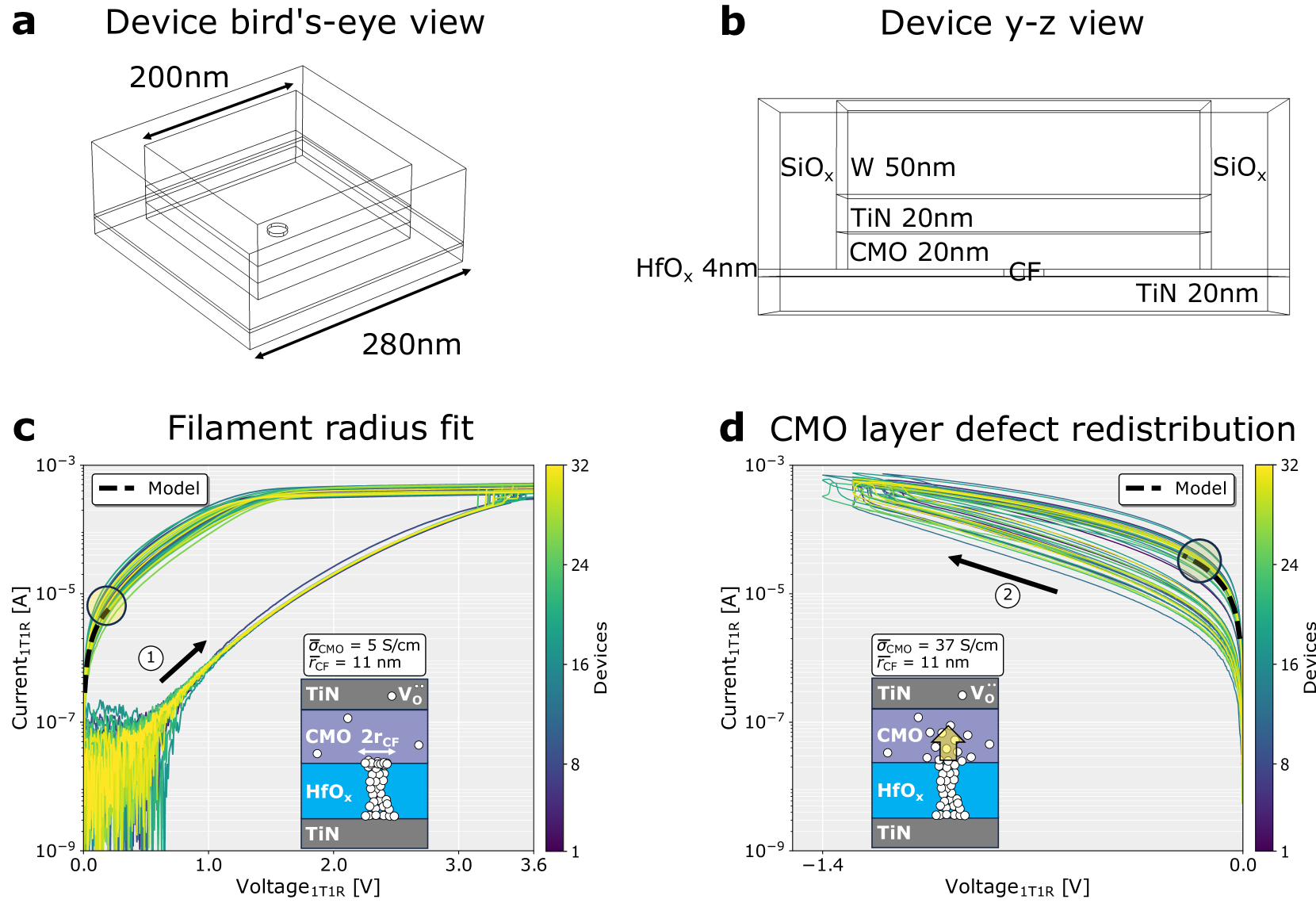
### Visual Description
## Device Schematics and Electrical Characteristics
### Overview
The image presents device schematics and electrical characteristics related to a resistive switching memory device. It includes two device views (bird's-eye and y-z) and two plots showing the current-voltage (I-V) characteristics for multiple devices under different conditions.
### Components/Axes
**Panel a: Device bird's-eye view**
* Title: Device bird's-eye view
* Dimensions: 200 nm x 280 nm (approximate)
**Panel b: Device y-z view**
* Title: Device y-z view
* Layers (from top to bottom):
* SiO<sub>x</sub>, W 50nm, SiO<sub>x</sub>
* TiN 20nm
* CMO 20nm
* CF (Conductive Filament)
* TiN 20nm
* HfO<sub>x</sub> 4nm
**Panel c: Filament radius fit**
* Title: Filament radius fit
* X-axis: Voltage<sub>1T1R</sub> [V]
* Scale: Linear, from 0.0 to 3.6
* Y-axis: Current<sub>1T1R</sub> [A]
* Scale: Logarithmic, from 10<sup>-9</sup> to 10<sup>-3</sup>
* Right Y-axis: Devices
* Scale: Linear, from 1 to 32
* Legend:
* Model (black dashed line)
* Inset Diagram:
* Layers (from top to bottom): TiN, CMO, HfO<sub>x</sub>, TiN
* Annotations: V<sub>O</sub><sup>••</sup>, 2r<sub>CF</sub>
* Parameters: σ<sub>CMO</sub> = 5 S/cm, r<sub>CF</sub> = 11 nm
* Arrow 1: Indicates the general trend of the I-V curves.
**Panel d: CMO layer defect redistribution**
* Title: CMO layer defect redistribution
* X-axis: Voltage<sub>1T1R</sub> [V]
* Scale: Linear, from -1.4 to 0.0
* Y-axis: Current<sub>1T1R</sub> [A]
* Scale: Logarithmic, from 10<sup>-9</sup> to 10<sup>-3</sup>
* Right Y-axis: Devices
* Scale: Linear, from 1 to 32
* Legend:
* Model (black dashed line)
* Inset Diagram:
* Layers (from top to bottom): TiN, CMO, HfO<sub>x</sub>, TiN
* Annotations: V<sub>O</sub><sup>••</sup>
* Parameters: σ<sub>CMO</sub> = 37 S/cm, r<sub>CF</sub> = 11 nm
* Arrow 2: Indicates the general trend of the I-V curves.
### Content Details
**Panel c: Filament radius fit**
* The plot shows multiple I-V curves, each representing a different device. The color of each curve corresponds to the number of devices, ranging from dark blue (1 device) to yellow (32 devices).
* The I-V curves generally show an increase in current with increasing voltage.
* At low voltages (near 0V), the current is very low (around 10<sup>-9</sup> A).
* As the voltage increases, the current increases sharply, reaching values around 10<sup>-3</sup> A at higher voltages (around 3.6V).
* The "Model" curve (black dashed line) represents a theoretical fit to the experimental data. It closely follows the average trend of the I-V curves.
* The inset diagram illustrates the device structure with the conductive filament (CF) formation in the HfO<sub>x</sub> layer. The CMO layer is also shown with oxygen vacancies (V<sub>O</sub><sup>••</sup>).
* The conductivity of the CMO layer (σ<sub>CMO</sub>) is given as 5 S/cm, and the radius of the conductive filament (r<sub>CF</sub>) is 11 nm.
**Panel d: CMO layer defect redistribution**
* Similar to panel c, this plot shows multiple I-V curves for different devices, colored according to the number of devices.
* The voltage range is from -1.4V to 0.0V.
* The I-V curves show a general decrease in current as the voltage becomes more negative.
* The current values range from around 10<sup>-3</sup> A at 0V to lower values (around 10<sup>-9</sup> A) at -1.4V.
* The "Model" curve (black dashed line) represents a theoretical fit to the experimental data.
* The inset diagram illustrates the device structure with the CMO layer defect redistribution. The CMO layer is shown with oxygen vacancies (V<sub>O</sub><sup>••</sup>).
* The conductivity of the CMO layer (σ<sub>CMO</sub>) is given as 37 S/cm, and the radius of the conductive filament (r<sub>CF</sub>) is 11 nm.
### Key Observations
* The device schematics in panels a and b provide a visual representation of the device structure and dimensions.
* The I-V curves in panels c and d show the electrical characteristics of the device under different conditions.
* The conductivity of the CMO layer (σ<sub>CMO</sub>) is different in panels c and d (5 S/cm vs. 37 S/cm), indicating a change in the material properties.
* The radius of the conductive filament (r<sub>CF</sub>) is the same in both panels (11 nm).
* The "Model" curves provide a theoretical fit to the experimental data, which can be used to understand the underlying physical mechanisms.
### Interpretation
The data suggests that the resistive switching behavior of the device is influenced by the CMO layer and the formation/redistribution of oxygen vacancies. The change in conductivity of the CMO layer between panels c and d indicates that the material properties are being modified, possibly due to the redistribution of defects. The conductive filament formation in the HfO<sub>x</sub> layer plays a crucial role in the switching mechanism. The I-V curves show the relationship between voltage and current, which is essential for understanding the device's performance. The "Model" curves provide a theoretical framework for interpreting the experimental data and understanding the underlying physical mechanisms. The difference in the CMO conductivity between the two plots suggests that the defect redistribution process significantly impacts the device's electrical characteristics.
</details>
Figure S1: ReRAM forming modelling. The CMO/HfO x ReRAM device is simulated using a 3D FEM in COMSOL Multiphysics 5.2 software. a The bird’s-eye view and b the lateral y-z view of the device’s geometry and material stack are shown. Due to the temperature and electric field confinement, an effective device area of 200 $×$ 200 nm 2 is considered for the simulation to reduce computational resource demands. c The experimental array forming data in the low-voltage linear regime (from 0 to $0.2\,\mathrm{V}$ ) are fitted to extract the average filament radius. d The increase in experimental conductance resulting from a negative voltage sweep after the forming event is modelled as an effective increase in the electrical conductivity of the CMO layer, due to a radial redistribution of defects.
<details>
<summary>x8.png Details</summary>
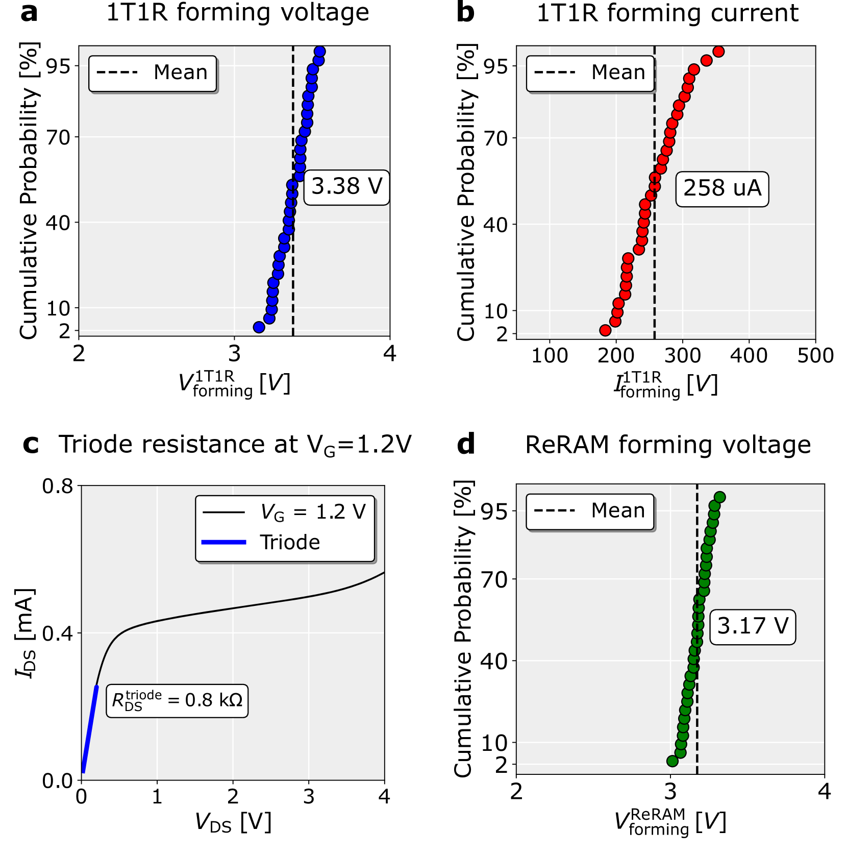
### Visual Description
## Chart Compilation: Electrical Characteristics of 1T1R and ReRAM Devices
### Overview
The image presents four plots (a, b, c, d) illustrating the electrical characteristics of 1T1R (One Transistor One Resistor) and ReRAM (Resistive Random-Access Memory) devices. Plots a, b, and d show cumulative probability distributions for forming voltage and current, while plot c depicts the triode resistance at a specific gate voltage.
### Components/Axes
**Plot a: 1T1R forming voltage**
* **Title:** 1T1R forming voltage
* **X-axis:** V<sup>1T1R</sup><sub>forming</sub> [V] (1T1R Forming Voltage in Volts). Scale ranges from 2 to 4, with tick marks at every 1 unit.
* **Y-axis:** Cumulative Probability [%]. Scale ranges from 2 to 95, with tick marks at 10, 40, 70, and 95.
* **Data:** Blue dots represent the cumulative probability of the forming voltage.
* **Mean:** Dashed black vertical line indicating the mean forming voltage.
* **Annotation:** "Mean" in a rounded box at the top-left.
* **Value Label:** A rounded box indicates a voltage of 3.38 V.
**Plot b: 1T1R forming current**
* **Title:** 1T1R forming current
* **X-axis:** I<sup>1T1R</sup><sub>forming</sub> [uA] (1T1R Forming Current in microAmperes). Scale ranges from 100 to 500, with tick marks at every 100 units.
* **Y-axis:** Cumulative Probability [%]. Scale ranges from 2 to 95, with tick marks at 10, 40, 70, and 95.
* **Data:** Red dots represent the cumulative probability of the forming current.
* **Mean:** Dashed black vertical line indicating the mean forming current.
* **Annotation:** "Mean" in a rounded box at the top-left.
* **Value Label:** A rounded box indicates a current of 258 uA.
**Plot c: Triode resistance at V<sub>G</sub>=1.2V**
* **Title:** Triode resistance at V<sub>G</sub>=1.2V
* **X-axis:** V<sub>DS</sub> [V] (Drain-Source Voltage in Volts). Scale ranges from 0 to 4, with tick marks at every 1 unit.
* **Y-axis:** I<sub>DS</sub> [mA] (Drain-Source Current in milliAmperes). Scale ranges from 0.0 to 0.8, with tick marks at 0.0, 0.4, and 0.8.
* **Data:**
* Black line represents V<sub>G</sub> = 1.2 V.
* Blue line represents the Triode region.
* **Legend:** Located at the top-right, indicating the black line as "V<sub>G</sub> = 1.2 V" and the blue line as "Triode".
* **Annotation:** "R<sup>triode</sup><sub>DS</sub> = 0.8 kΩ" in a rounded box, indicating the triode resistance.
**Plot d: ReRAM forming voltage**
* **Title:** ReRAM forming voltage
* **X-axis:** V<sup>ReRAM</sup><sub>forming</sub> [V] (ReRAM Forming Voltage in Volts). Scale ranges from 2 to 4, with tick marks at every 1 unit.
* **Y-axis:** Cumulative Probability [%]. Scale ranges from 2 to 95, with tick marks at 10, 40, 70, and 95.
* **Data:** Green dots represent the cumulative probability of the forming voltage.
* **Mean:** Dashed black vertical line indicating the mean forming voltage.
* **Annotation:** "Mean" in a rounded box at the top-left.
* **Value Label:** A rounded box indicates a voltage of 3.17 V.
### Detailed Analysis
**Plot a: 1T1R forming voltage**
* The cumulative probability increases sharply between 3 V and 3.5 V.
* The mean forming voltage is approximately 3.38 V.
**Plot b: 1T1R forming current**
* The cumulative probability increases sharply between 200 uA and 300 uA.
* The mean forming current is approximately 258 uA.
**Plot c: Triode resistance at V<sub>G</sub>=1.2V**
* The blue line (Triode) shows a linear relationship between V<sub>DS</sub> and I<sub>DS</sub> up to approximately 0.5 V.
* The black line (V<sub>G</sub> = 1.2 V) shows a non-linear relationship, with the current increasing at a decreasing rate as V<sub>DS</sub> increases.
* The triode resistance is given as 0.8 kΩ.
**Plot d: ReRAM forming voltage**
* The cumulative probability increases sharply between 3 V and 3.2 V.
* The mean forming voltage is approximately 3.17 V.
### Key Observations
* The forming voltages for both 1T1R and ReRAM devices are clustered around 3 V, with 1T1R having a slightly higher mean forming voltage.
* The forming current for 1T1R devices is centered around 250 uA.
* The triode region of the transistor exhibits a linear I-V relationship, while the saturation region shows a non-linear behavior.
### Interpretation
The data suggests that the forming process for both 1T1R and ReRAM devices requires a specific voltage range to initiate the resistive switching. The relatively narrow distribution of forming voltages indicates a consistent and controlled fabrication process. The triode resistance plot provides insight into the transistor's behavior, showing the linear and non-linear regions of operation. The 1T1R device has a higher forming voltage and current compared to the ReRAM device, which could be attributed to differences in their material composition or device structure.
</details>
Figure S2: Experimental CMO/HfO x ReRAM array forming data. a The forming voltage distribution of the 1T1R cells within the array, defined as the voltage required to trigger the highest current increase during the quasi-static voltage sweep from 0 to $3.6\,\mathrm{V}$ in Fig. 2 a of the manuscript. b The array forming current distribution corresponding to $V=V_{\mathrm{forming}}^{\mathrm{1T1R}}$ . c The experimental resistance of the transistor in the triode region at $V_{\mathrm{G}}=\mathrm{1.2\,V}$ , extracted from a linear fit from 0 to $0.2\,\mathrm{V}$ of the transistor output characteristic. d The forming voltage distribution of the ReRAM array, shown in Fig. 2 c of the manuscript, computed as $V_{\mathrm{forming}}^{\mathrm{ReRAM}}$ = $V_{\mathrm{forming}}^{\mathrm{1T1R}}$ - $R_{\mathrm{DS}}^{\mathrm{triode}}$ * $I_{\mathrm{forming}}^{\mathrm{1T1R}}$ .
<details>
<summary>x9.png Details</summary>
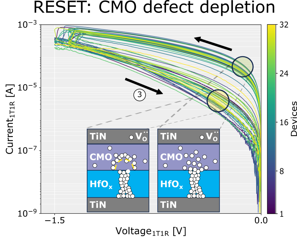
### Visual Description
## IV Curve: RESET: CMO defect depletion
### Overview
The image shows a plot of current (I) versus voltage (V) characteristics for multiple devices, illustrating the RESET process in a CMO (presumably a complex metal oxide) defect depletion scenario. The plot includes a color bar indicating the number of devices, ranging from 1 to 32. Insets show diagrams of the device structure with defect distribution.
### Components/Axes
* **Title:** RESET: CMO defect depletion
* **Y-axis:** Current$_{1T1R}$ [A] (logarithmic scale from 10$^{-9}$ to 10$^{-3}$)
* **X-axis:** Voltage$_{1T1R}$ [V] (linear scale from -1.5 to 0.0)
* **Colorbar:** Devices (ranging from 1 to 32, with color gradient from dark purple to yellow)
* **Diagram Insets:** Two diagrams showing the device structure with layers of TiN, CMO, and HfO$_x$, and the distribution of oxygen vacancies (Vö).
### Detailed Analysis
* **Y-Axis (Current):** The y-axis is a logarithmic scale representing the current, ranging from 10$^{-9}$ A to 10$^{-3}$ A. The grid lines are spaced at each order of magnitude.
* **X-Axis (Voltage):** The x-axis represents the voltage, ranging from -1.5 V to 0.0 V. The grid lines are spaced at 0.5 V intervals.
* **Data Series:** There are multiple curves plotted on the graph, each representing a device. The color of each curve corresponds to the number of devices, as indicated by the colorbar.
* **Colorbar (Devices):** The colorbar on the right side of the plot indicates the number of devices, ranging from 1 (dark purple) to 32 (yellow). The color gradient shows a continuous transition between these values. The colorbar has labeled ticks at 1, 8, 16, 24, and 32.
* **Diagram Insets:**
* Each inset shows a stack of materials: TiN (Titanium Nitride), CMO (Complex Metal Oxide), and HfO$_x$ (Hafnium Oxide).
* The left diagram shows a sparse distribution of white circles (representing defects or oxygen vacancies) in the CMO layer and a concentrated region of defects in the HfO$_x$ layer. An arrow indicates the movement of defects from the CMO to the HfO$_x$ layer.
* The right diagram shows a depleted CMO layer and a more concentrated region of defects in the HfO$_x$ layer.
* "Vö" is labeled near the top of the CMO layer, indicating oxygen vacancies.
* **Arrows:** Two black arrows are present on the main chart, indicating the direction of the RESET process.
* **Number 3:** A circled number "3" is present on the main chart, near the center.
* **Curve Trends:**
* The curves generally start at a low current level (around 10$^{-9}$ A) at a voltage of -1.5 V.
* As the voltage increases towards 0 V, the current initially remains low.
* At a certain voltage (varying between -1.5V and -0.5V), the current abruptly increases, indicating the RESET process.
* The curves then converge towards a higher current level (around 10$^{-3}$ A) as the voltage approaches 0 V.
* The color of the curves varies from dark purple to yellow, indicating different numbers of devices exhibiting similar behavior.
### Key Observations
* The RESET process is characterized by a sudden increase in current at a specific voltage.
* The voltage at which the RESET occurs varies between devices.
* The number of devices influences the density of curves, with yellow curves representing a higher number of devices.
* The diagrams illustrate the redistribution of defects during the RESET process, with defects moving from the CMO layer to the HfO$_x$ layer.
### Interpretation
The data suggests that the RESET process in the CMO device involves the depletion of defects (likely oxygen vacancies) in the CMO layer and their accumulation in the HfO$_x$ layer. The IV curves show that the voltage required to trigger the RESET process varies between devices, possibly due to variations in the initial defect distribution or material properties. The color-coding of the curves indicates that the observed behavior is consistent across multiple devices, with some devices exhibiting more pronounced RESET characteristics than others. The diagrams provide a visual representation of the defect redistribution mechanism, supporting the interpretation of the IV curves. The arrows on the main chart indicate the direction of the RESET process, showing the change in current as the voltage increases.
</details>
Figure S3: The experimental array’s response to the voltage sweep from 0 to $-1.5\,\mathrm{V}$ , following the positive forming and the initial negative voltage sweep (denoted as step (1) and (2) in Fig. 2 a of the manuscript, respectively). The oxygen vacancies in the CMO layer radially spread outward, depleting the CMO defect sub-band within a half-spherical volume at the interface with the conductive filament, leading to a reset process.
<details>
<summary>x10.png Details</summary>
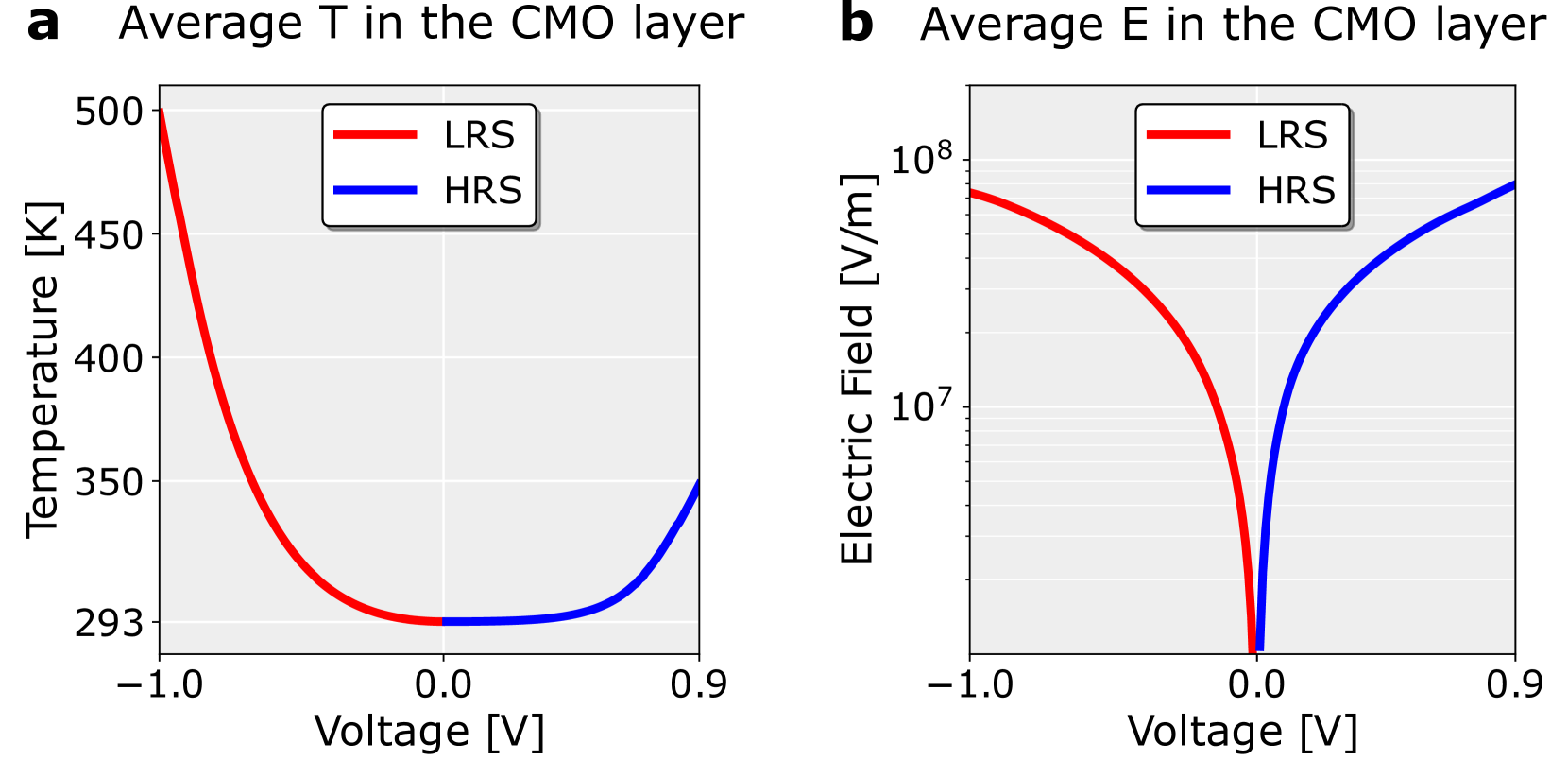
### Visual Description
## Chart: Average Temperature and Electric Field in CMO Layer vs. Voltage
### Overview
The image presents two line graphs comparing the average temperature (T) and electric field (E) in the CMO layer as a function of voltage. The graphs show the behavior of two states: Low Resistance State (LRS) and High Resistance State (HRS). The left graph displays temperature in Kelvin (K), while the right graph displays the electric field in Volts per meter (V/m) on a logarithmic scale.
### Components/Axes
**Left Graph (Average T in the CMO layer):**
* **Title:** a Average T in the CMO layer
* **Y-axis:** Temperature [K]
* Scale: Linear, ranging from approximately 293 K to 500 K.
* Markers: 293, 350, 400, 450, 500
* **X-axis:** Voltage [V]
* Scale: Linear, ranging from -1.0 V to 0.9 V.
* Markers: -1.0, 0.0, 0.9
* **Legend:** Located in the top-right corner.
* LRS (Low Resistance State): Represented by a red line.
* HRS (High Resistance State): Represented by a blue line.
**Right Graph (Average E in the CMO layer):**
* **Title:** b Average E in the CMO layer
* **Y-axis:** Electric Field [V/m]
* Scale: Logarithmic (base 10), ranging from approximately 10^7 to 10^8 V/m.
* Markers: 10^7, 10^8
* **X-axis:** Voltage [V]
* Scale: Linear, ranging from -1.0 V to 0.9 V.
* Markers: -1.0, 0.0, 0.9
* **Legend:** Located in the top-right corner.
* LRS (Low Resistance State): Represented by a red line.
* HRS (High Resistance State): Represented by a blue line.
### Detailed Analysis
**Left Graph (Average T in the CMO layer):**
* **LRS (Red Line):**
* Trend: Starts at approximately 500 K at -1.0 V, decreases rapidly to approximately 293 K near 0.0 V.
* Data Points:
* (-1.0 V, 500 K)
* (0.0 V, 293 K)
* **HRS (Blue Line):**
* Trend: Remains constant at approximately 293 K from 0.0 V to -0.2V, then increases to approximately 340 K at 0.9 V.
* Data Points:
* (0.0 V, 293 K)
* (0.9 V, 340 K)
**Right Graph (Average E in the CMO layer):**
* **LRS (Red Line):**
* Trend: Starts at approximately 10^8 V/m at -1.0 V, decreases rapidly to approximately 10^7 V/m near 0.0 V.
* Data Points:
* (-1.0 V, 10^8 V/m)
* (0.0 V, 10^7 V/m)
* **HRS (Blue Line):**
* Trend: Starts at approximately 10^7 V/m at 0.0 V, increases rapidly to approximately 8 * 10^7 V/m at 0.9 V.
* Data Points:
* (0.0 V, 10^7 V/m)
* (0.9 V, 8 * 10^7 V/m)
### Key Observations
* In the temperature graph, the LRS exhibits a significant temperature drop as voltage approaches 0 V, while the HRS maintains a relatively constant low temperature.
* In the electric field graph, the LRS shows a sharp decrease in electric field as voltage approaches 0 V, while the HRS shows a sharp increase in electric field as voltage increases from 0 V to 0.9 V.
* Both graphs show a distinct change in behavior around 0 V, suggesting a switching point or transition region between the two resistance states.
### Interpretation
The graphs illustrate the relationship between voltage, temperature, and electric field within the CMO layer for two distinct resistance states (LRS and HRS). The data suggests that the LRS is characterized by high temperature and high electric field at negative voltages, which rapidly decrease as the voltage approaches zero. Conversely, the HRS maintains a low temperature and low electric field near zero voltage, with the electric field increasing as the voltage becomes more positive. This behavior is indicative of a voltage-controlled switching mechanism within the CMO layer, where the material transitions between high and low resistance states depending on the applied voltage. The sharp changes observed near 0 V suggest a critical voltage threshold for this switching behavior.
</details>
Figure S4: The voltage-dependent evolution of a the average temperature and b electric field within a 3D half-spherical volume of the CMO layer situated atop the conductive filament in both HRS and LRS is presented. These trends serve as inputs for equation (6) of the manuscript.
<details>
<summary>x11.png Details</summary>
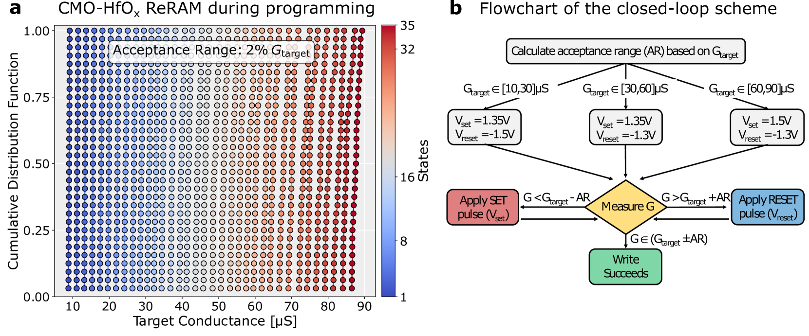
### Visual Description
## Chart/Diagram Type: Compound Image - Heatmap and Flowchart
### Overview
The image consists of two sub-figures: (a) a heatmap showing the cumulative distribution function of a CMO-HfOₓ ReRAM during programming, and (b) a flowchart illustrating the closed-loop scheme used in the programming process.
### Components/Axes
**Sub-figure (a): Heatmap**
* **Title:** CMO-HfOₓ ReRAM during programming
* **X-axis:** Target Conductance [µS]
* Scale: 10 to 90 µS, with tick marks every 10 µS (10, 20, 30, 40, 50, 60, 70, 80, 90)
* **Y-axis:** Cumulative Distribution Function
* Scale: 0.00 to 1.00, with tick marks every 0.25 (0.00, 0.25, 0.50, 0.75, 1.00)
* **Colorbar (right side):** States
* Scale: 1 to 35, with tick marks at 1, 8, 16, 32, and 35. The color gradient ranges from blue (low states) to red (high states).
* **Annotation:** "Acceptance Range: 2% Gtarget" located near the top of the heatmap.
**Sub-figure (b): Flowchart**
* **Title:** Flowchart of the closed-loop scheme
* **Nodes:**
* Calculate acceptance range (AR) based on Gtarget (top)
* Gtarget ∈ [10,30]µS
* Vset = 1.35V
* Vreset = -1.5V
* Gtarget ∈ [30,60]µS
* Vset = 1.35V
* Vreset = -1.3V
* Gtarget ∈ [60,90]µS
* Vset = 1.5V
* Vreset = -1.3V
* Apply SET pulse (Vset) (red rounded rectangle)
* Measure G (yellow diamond)
* Apply RESET pulse (Vreset) (blue rounded rectangle)
* Write Succeeds (green rounded rectangle)
* **Edges:** Arrows indicating the flow of the process.
* **Conditions:**
* G < Gtarget - AR
* G > Gtarget + AR
* G ∈ (Gtarget ± AR)
### Detailed Analysis or Content Details
**Sub-figure (a): Heatmap**
* The heatmap shows the distribution of states for different target conductance values.
* At lower target conductance values (around 10-30 µS), the cumulative distribution function tends to have lower state values (blue color).
* As the target conductance increases (towards 80-90 µS), the cumulative distribution function shifts towards higher state values (red color).
* The color gradient indicates a gradual transition from low to high states as the target conductance increases.
* The "Acceptance Range" annotation indicates a tolerance of 2% around the target conductance.
**Sub-figure (b): Flowchart**
* The flowchart describes an iterative process for programming the ReRAM.
* The process starts by calculating the acceptance range (AR) based on the target conductance (Gtarget).
* Depending on the range of Gtarget, different SET and RESET voltages are applied.
* The conductance (G) is measured, and based on whether it's within the acceptance range (Gtarget ± AR), either a SET or RESET pulse is applied, or the write is considered successful.
* The process loops back to the "Measure G" step until the desired conductance is achieved.
### Key Observations
* The heatmap shows a clear correlation between target conductance and the distribution of states.
* The flowchart illustrates a closed-loop feedback mechanism for precise control of the ReRAM programming.
* The acceptance range (2% Gtarget) plays a crucial role in determining the success of the programming.
### Interpretation
The data suggests that the CMO-HfOₓ ReRAM programming process is controllable and predictable. The heatmap demonstrates that the target conductance significantly influences the resulting state distribution. The closed-loop scheme, as depicted in the flowchart, allows for fine-tuning of the ReRAM's conductance by iteratively applying SET and RESET pulses based on the measured conductance value and the defined acceptance range. This feedback mechanism ensures that the ReRAM is programmed to the desired state with high precision. The different voltage levels for different Gtarget ranges suggest an optimization strategy to improve programming efficiency and accuracy.
</details>
Figure S5: a The experimental cumulative distribution of conductance values for 35 representative programmed levels using 2% of G target as acceptance range. The closed-loop scheme based on identical pulses shown in Fig. 3 b of the manuscript and detailed in Methods is used. b Flowchart illustrating the identical-pulse closed-loop technique used for programming the ReRAM array into target analog conductance range.
<details>
<summary>x12.png Details</summary>
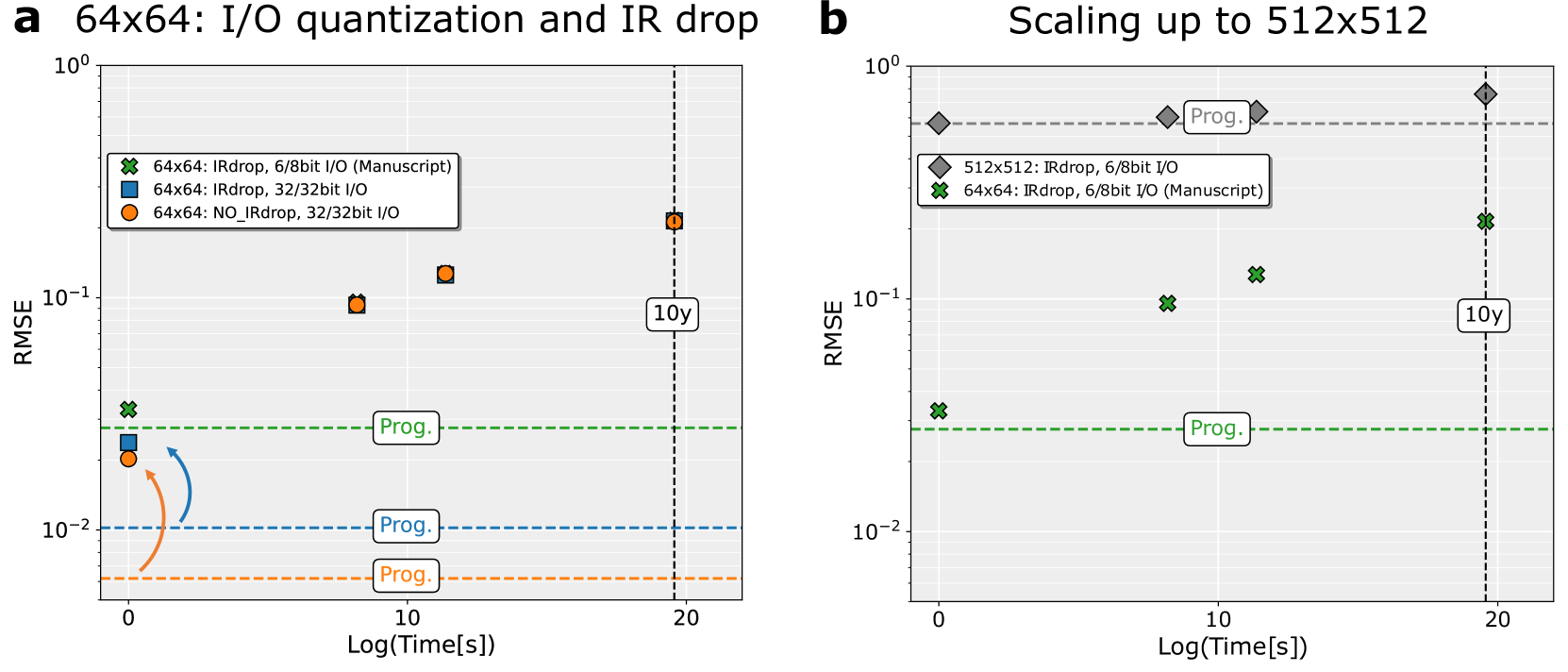
### Visual Description
## Chart: I/O Quantization and IR Drop vs. Scaling
### Overview
The image presents two scatter plots comparing Root Mean Square Error (RMSE) against Log(Time[s]) for different I/O configurations and scaling factors. Plot 'a' focuses on 64x64 resolution with varying I/O quantization and IR drop settings, while plot 'b' compares 64x64 and 512x512 resolutions with a specific I/O configuration. Both plots include horizontal dashed lines labeled "Prog." and a vertical dashed line labeled "10y".
### Components/Axes
**Plot a: 64x64: I/O quantization and IR drop**
* **X-axis:** Log(Time[s]), with tick marks at 0, 10, and 20.
* **Y-axis:** RMSE, with a logarithmic scale ranging from 10^-2 to 10^0.
* **Legend (top-left):**
* Green 'x': 64x64: IRdrop, 6/8bit I/O (Manuscript)
* Blue square: 64x64: IRdrop, 32/32bit I/O
* Orange circle: 64x64: NO\_IRdrop, 32/32bit I/O
* **Horizontal Dashed Lines:**
* Green: "Prog." located near y = 0.03
* Blue: "Prog." located near y = 0.01
* Orange: "Prog." located near y = 0.006
* **Vertical Dashed Line:** Located at x = 20, labeled "10y".
**Plot b: Scaling up to 512x512**
* **X-axis:** Log(Time[s]), with tick marks at 0, 10, and 20.
* **Y-axis:** RMSE, with a logarithmic scale ranging from 10^-2 to 10^0.
* **Legend (top-right):**
* Gray diamond: 512x512: IRdrop, 6/8bit I/O
* Green 'x': 64x64: IRdrop, 6/8bit I/O (Manuscript)
* **Horizontal Dashed Lines:**
* Green: "Prog." located near y = 0.03
* Gray: "Prog." located near y = 0.6
* **Vertical Dashed Line:** Located at x = 20, labeled "10y".
### Detailed Analysis
**Plot a: 64x64: I/O quantization and IR drop**
* **64x64: IRdrop, 6/8bit I/O (Manuscript) (Green 'x'):**
* At x=0, RMSE ≈ 0.03
* At x=20, RMSE ≈ 0.03
* Trend: Relatively constant.
* **64x64: IRdrop, 32/32bit I/O (Blue square):**
* At x=0, RMSE ≈ 0.02
* At x=10, RMSE ≈ 0.09
* At x=20, RMSE ≈ 0.13
* Trend: Increasing.
* **64x64: NO\_IRdrop, 32/32bit I/O (Orange circle):**
* At x=0, RMSE ≈ 0.015
* At x=10, RMSE ≈ 0.09
* At x=20, RMSE ≈ 0.18
* Trend: Increasing.
**Plot b: Scaling up to 512x512**
* **512x512: IRdrop, 6/8bit I/O (Gray diamond):**
* At x=0, RMSE ≈ 0.6
* At x=10, RMSE ≈ 0.6
* At x=20, RMSE ≈ 0.7
* Trend: Relatively constant.
* **64x64: IRdrop, 6/8bit I/O (Manuscript) (Green 'x'):**
* At x=0, RMSE ≈ 0.03
* At x=10, RMSE ≈ 0.09
* At x=20, RMSE ≈ 0.1
* Trend: Increasing.
### Key Observations
* In plot 'a', increasing the bit depth from 6/8 to 32/32 for the 64x64 resolution, while keeping IRdrop, results in a higher RMSE as Log(Time[s]) increases. Removing IRdrop also results in a higher RMSE.
* In plot 'b', scaling up to 512x512 with 6/8bit I/O and IRdrop leads to a significantly higher RMSE compared to the 64x64 configuration with the same settings.
* The "Prog." lines seem to represent some kind of performance target or threshold.
* The "10y" line at Log(Time[s]) = 20 likely indicates a specific time point of interest (10 years).
### Interpretation
The plots suggest that I/O quantization and IR drop significantly impact the RMSE, especially as the simulation time increases. For the 64x64 resolution, using lower bit depths (6/8) and including IR drop results in lower RMSE values compared to higher bit depths (32/32) or removing IR drop. Scaling up to 512x512 dramatically increases the RMSE, indicating a potential trade-off between resolution and accuracy for the given I/O configuration. The "Prog." lines likely represent acceptable error thresholds, and the data indicates whether each configuration meets those thresholds. The "10y" marker suggests a long-term performance evaluation point.
</details>
Figure S6: The individual impact of IR-drop across array wires and input/output bit quantization on MVM accuracy. a Simulated RMSE compared to FP ideal results using 64x64 analog CMO/HfOx ReRAM array, shown as a function of the time after programming. Dashed horizontal lines represent the RMSE during programming, considering programming noise (with 0.2% G target as the acceptance range) but excluding relaxation effects. With 32-bit input/output quantization and no IR-drop (orange dots), an RMSE as low as 6 $10^{-3}$ is achieved during programming, which immediately increases (see the arrow) after relaxation (within $\mathrm{1\,s}$ ). Including the realistic IR-drop results in an overall RMSE increase (blue squares). Finally, reducing input/output quantization to 6/8 bits, respectively, leads to a further accuracy loss (green crosses), demonstrating that at short timescales (within 1 hour), the main analog MVM accuracy bottleneck is the reduced input/output quantization. After 1 hour, all cases converge, showing that the accuracy bottleneck is then dominated by the relaxation process. b By scaling up to a 512x512 array size (grey diamonds) and considering input/output quantization of 6/8 bits, IR-drop emerges as the primary bottleneck for analog MVM accuracy.
<details>
<summary>x13.png Details</summary>
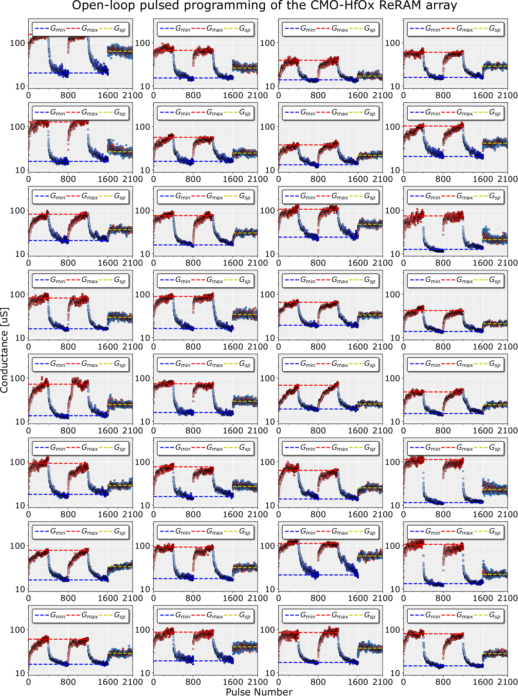
### Visual Description
## Chart: Open-loop pulsed programming of the CMO-HfOx ReRAM array
### Overview
The image presents a series of 30 plots arranged in a 6x5 grid, each displaying the conductance (in uS) of a CMO-HfOx ReRAM array element as a function of the pulse number. Each plot shows a similar trend: the conductance starts at a high level, drops to a lower level after a number of pulses, and then returns to a stable intermediate level. The plots also include horizontal dashed lines representing Gmin, Gmax, and Gsp.
### Components/Axes
* **Title:** Open-loop pulsed programming of the CMO-HfOx ReRAM array
* **Y-axis:** Conductance [uS]. The scale is logarithmic, ranging from 10 to 100.
* **X-axis:** Pulse Number. The scale is linear, ranging from 0 to 2100, with major ticks at 0, 800, 1600, and 2100.
* **Legend:** Located at the top of each subplot.
* Gmin: Blue dashed line
* Gmax: Red dashed line
* Gsp: Yellow dashed line
### Detailed Analysis
Each of the 30 subplots displays a similar trend. The conductance starts near the Gmax level (red dashed line), then drops rapidly to near the Gmin level (blue dashed line) after a number of pulses (approximately 800). After more pulses (approximately 1600), the conductance stabilizes near the Gsp level (yellow dashed line).
* **Gmin:** The blue dashed line is consistently around 10 uS.
* **Gmax:** The red dashed line is consistently around 100 uS.
* **Gsp:** The yellow dashed line is consistently between 20 and 40 uS.
The data points are represented by circles, with color varying from red to blue, indicating the change in conductance.
### Key Observations
* The conductance switching behavior is consistent across all 30 ReRAM array elements.
* The switching occurs in two distinct phases: a rapid drop from Gmax to Gmin, followed by a stabilization at Gsp.
* There is some variability in the exact number of pulses required for the initial drop in conductance.
### Interpretation
The data suggests that the CMO-HfOx ReRAM array exhibits reliable and repeatable switching behavior under open-loop pulsed programming. The consistent trends across all 30 elements indicate uniformity in the device characteristics. The two-phase switching behavior may be related to different physical mechanisms involved in the conductance change. The Gsp level represents a stable intermediate state that the device settles into after the initial switching event. The variability in the number of pulses required for the initial drop could be due to slight variations in the device fabrication or operating conditions.
</details>
Figure S7: The experimental response of the 8x4 CMO/HfO x ReRAM devices within the array to the open-loop programming pulse scheme (shown in Fig. 5 b of the manuscript) is shown. The set and reset pulse amplitudes are $1.35\,\mathrm{V}$ ( $V_{\mathrm{G}}=\mathrm{1.4\,V}$ ) and $-1.3\,\mathrm{V}$ ( $V_{\mathrm{G}}=\mathrm{3.3\,V}$ ), respectively, with a constant width of 2.5 µs due to setup limitations.
<details>
<summary>x14.png Details</summary>
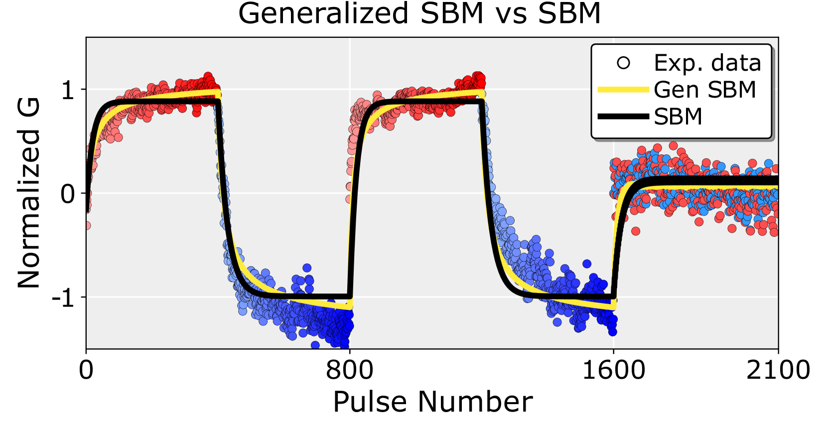
### Visual Description
## Chart: Generalized SBM vs SBM
### Overview
The image is a chart comparing the performance of a Standard Binding Model (SBM) and a Generalized SBM against experimental data. The chart plots "Normalized G" on the y-axis against "Pulse Number" on the x-axis. The experimental data is represented by scattered points, while the SBM and Generalized SBM are represented by lines. The experimental data points are colored, transitioning from blue to red as the pulse number increases within each pulse cycle.
### Components/Axes
* **Title:** Generalized SBM vs SBM
* **X-axis:** Pulse Number, with tick marks at 0, 800, 1600, and 2100.
* **Y-axis:** Normalized G, with tick marks at -1, 0, and 1.
* **Legend (Top-Right):**
* Exp. data (represented by open circles)
* Gen SBM (represented by a yellow line)
* SBM (represented by a black line)
### Detailed Analysis
* **Experimental Data (Exp. data):** The experimental data is shown as scattered points. The color of the points transitions from blue to red within each pulse cycle. The data shows a cyclical pattern, with rapid increases and decreases in "Normalized G" corresponding to the pulses.
* From Pulse Number 0 to approximately 400, the data points transition from blue to red as the Normalized G increases from approximately -1 to 1.
* From Pulse Number 400 to approximately 800, the data points transition from red to blue as the Normalized G decreases from approximately 1 to -1.
* From Pulse Number 800 to approximately 1200, the data points transition from blue to red as the Normalized G increases from approximately -1 to 1.
* From Pulse Number 1200 to approximately 1600, the data points transition from red to blue as the Normalized G decreases from approximately 1 to -1.
* From Pulse Number 1600 to 2100, the data points are a mix of red and blue, with the Normalized G fluctuating around 0.
* **Generalized SBM (Gen SBM):** The Generalized SBM is represented by a yellow line. It generally follows the trend of the experimental data, but with smoother transitions.
* From Pulse Number 0 to approximately 400, the yellow line increases from approximately -1 to 1.
* From Pulse Number 400 to approximately 800, the yellow line decreases from approximately 1 to -1.
* From Pulse Number 800 to approximately 1200, the yellow line increases from approximately -1 to 1.
* From Pulse Number 1200 to approximately 1600, the yellow line decreases from approximately 1 to -1.
* From Pulse Number 1600 to 2100, the yellow line fluctuates around 0.
* **SBM:** The SBM is represented by a black line. It shows sharp, step-like changes in "Normalized G".
* From Pulse Number 0 to approximately 400, the black line increases sharply from approximately -1 to 1.
* From Pulse Number 400 to approximately 800, the black line decreases sharply from approximately 1 to -1.
* From Pulse Number 800 to approximately 1200, the black line increases sharply from approximately -1 to 1.
* From Pulse Number 1200 to approximately 1600, the black line decreases sharply from approximately 1 to -1.
* From Pulse Number 1600 to 2100, the black line fluctuates around 0.
### Key Observations
* The experimental data exhibits a cyclical pattern corresponding to the pulses.
* The Generalized SBM provides a smoother approximation of the experimental data compared to the SBM.
* The SBM shows sharp transitions, indicating an idealized, step-like response.
* After pulse number 1600, the experimental data and the models converge around a Normalized G value of approximately 0.
### Interpretation
The chart compares the performance of two models (SBM and Generalized SBM) in predicting experimental data. The Generalized SBM appears to be a better fit for the experimental data, as it captures the smoother transitions observed in the data. The SBM, with its sharp transitions, represents a more idealized model that doesn't fully capture the nuances of the experimental data. The convergence of all three data sets after pulse number 1600 suggests a steady-state condition is reached. The color gradient in the experimental data suggests a time-dependent process within each pulse cycle, which the Generalized SBM captures better than the standard SBM.
</details>
Figure S8: The experimental open-loop pulsed response of a representative CMO/HfO x ReRAM device within the array shows that the potentiation and depression characteristics do not inherently saturate at the upper and lower boundaries. The generalized soft bounds model (yellow line) better captures this experimental trend compared to the saturated soft bounds model (black line).
<details>
<summary>x15.png Details</summary>
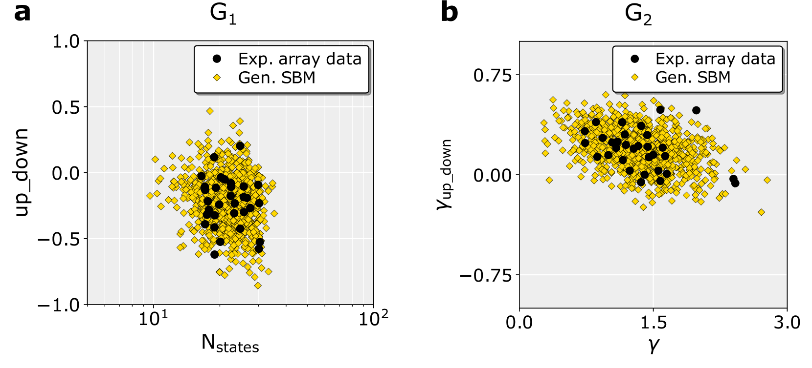
### Visual Description
## Scatter Plots: G1 vs. G2
### Overview
The image contains two scatter plots, labeled 'a' and 'b', displaying the relationship between different variables. Plot 'a' (G1) shows "up_down" against "N_states" (logarithmic scale), while plot 'b' (G2) shows "Y_up_down" against "Y". Each plot contains two data series: "Exp. array data" (black circles) and "Gen. SBM" (yellow diamonds).
### Components/Axes
**Plot a (G1):**
* **Title:** G1 (top-center)
* **X-axis:** N_states (bottom). Logarithmic scale from approximately 10^1 to 10^2.
* **Y-axis:** up_down (left). Linear scale from -1.0 to 1.0, with tick marks at -0.5, 0.0, and 0.5.
* **Legend:** Located in the top-right corner.
* Black circle: Exp. array data
* Yellow diamond: Gen. SBM
**Plot b (G2):**
* **Title:** G2 (top-center)
* **X-axis:** Y (bottom). Linear scale from 0.0 to 3.0, with a tick mark at 1.5.
* **Y-axis:** Y_up_down (left). Linear scale from -0.75 to 0.75, with a tick mark at 0.0.
* **Legend:** Located in the top-right corner.
* Black circle: Exp. array data
* Yellow diamond: Gen. SBM
### Detailed Analysis
**Plot a (G1):**
* **Exp. array data (black circles):** The data points are clustered around the center of the plot. The majority of the points are between N_states values of 10 and 20, and up_down values of -0.5 and 0.5.
* **Gen. SBM (yellow diamonds):** The data points are more spread out than the "Exp. array data". They form a cloud around the "Exp. array data", with some points extending to the edges of the plot.
**Plot b (G2):**
* **Exp. array data (black circles):** The data points are clustered around the center of the plot. The majority of the points are between Y values of 1.0 and 2.0, and Y_up_down values of 0.0 and 0.5.
* **Gen. SBM (yellow diamonds):** The data points are more spread out than the "Exp. array data". They form a cloud around the "Exp. array data", with some points extending to the edges of the plot. The data appears to have a slight negative correlation.
### Key Observations
* Both plots show a clustering of "Exp. array data" in the center, with "Gen. SBM" data points more dispersed around them.
* Plot 'a' has a logarithmic x-axis, while plot 'b' has a linear x-axis.
* Plot 'b' shows a slight negative correlation between Y and Y_up_down for the "Gen. SBM" data.
### Interpretation
The plots compare experimental array data with data generated using a Stochastic Block Model (SBM). The clustering of experimental data suggests a more constrained relationship between the variables, while the broader distribution of the generated data indicates a less constrained or more variable relationship. The negative correlation in plot 'b' for the generated data might indicate an inverse relationship between the variables in the model. The plots suggest that the SBM model captures some aspects of the experimental data but also introduces more variability.
</details>
Figure S9: Multi-variate Gaussian distributions to reproduce the experimental inter-device variability. a Multi-variate gaussian G1 distribution of the experimental number of states and device asymmetry ( $up\_down$ ). b Gaussian G2 distribution of the analytical parameters $\gamma$ and $\gamma_{\rm up\_down}$ extracted from the generalized soft bounds model fitting to the experimental traces.
Device modelling
$up\_down$ parameter
The $up\_down$ parameter is defined for the generalized soft bounds model in the simulation environment of the ‘aihwkit’ as the directional bias between the up and down update size ( $\Delta G^{+}$ and $\Delta G^{-}$ ). In addition, the minimum step in each direction d is described by the following expression [44].
$$
\displaystyle\Delta G^{d}=\Delta G_{SP}(1+d\beta+\sigma_{d-to-d}) \tag{7}
$$
where d is -1 or 1 depending on the update direction. In contrast, the symmetry point is defined for each device as follows [23]:
$$
\displaystyle SP=[\Delta G^{+}-\Delta G^{-}]/[\Delta G^{+}/(b_{\rm max}-\Delta
G%
^{+}/b_{\rm min})] \tag{8}
$$
Where $\Delta G^{+}$ , $\Delta G^{-}$ define the minimum step size in the up and down direction respectively, and $b_{\rm max}$ and $b_{\rm min}$ represent the upper and lower bounds of the conductance. Therefore, considering an independent definition of each device (i.e. zero d-to-d variability) and a normalized conductance range between -1 and 1, the symmetry point device-level characteristic and the $up\_down$ analytical parameter are equivalent.
Training setup
For result replicability, the experimental parameters are incorporated into the simulation environment, where the Noise-to-Signal Ratio (NSR) is represented by ’dw_min_std’, normalized SP by ‘up_down’, normalized maximum and minimum conductances by ‘w_max’ and ‘w_min’ and min conductance step by ‘dw_min’. From this device model, analog training simulations were performed using AGAD considering a learning rate to update the weights of 1e-2, ‘fast_lr’ of 0.1 to update matrix, ‘transfer_every’ 3 iterations and batch size of 32. The FP baseline was obtained with SGD training using a learning rate of 1e-3 and batch size of 32.