# Rethinking Compute Substrates for 3D-Stacked Near-Memory LLM Decoding: Microarchitecture–Scheduling Co-Design
**Authors**: Chenyang Ai, Yixing Zhang, Haoran Wu, Yudong Pan, Lechuan Zhao, Wenhui OU
> University of Edinburgh Edinburgh United Kingdom
> Peking University Beijing China
> University of Cambridge Cambridge United Kingdom
> University of Chinese Academy of Sciences Beijing China
> The Hong Kong University of Science and Technology Hong Kong China
## Abstract
Large language model (LLM) decoding is a major inference bottleneck because its low arithmetic intensity makes performance highly sensitive to memory bandwidth. 3D-stacked near-memory processing (NMP) provides substantially higher local memory bandwidth than conventional off-chip interfaces, making it a promising substrate for decode acceleration. However, our analysis shows that this bandwidth advantage also shifts many decode operators on 3D-stacked NMP back into the compute-bound regime. Under the tight area budget of the logic die, the design of the compute substrate itself therefore becomes a first-order challenge.
Therefore, we rethink the compute microarchitecture of prior 3D-stacked NMP designs. First, we replace prior MAC tree-based compute units with a more area-efficient systolic array, and we further observe that decode operators exhibit substantial shape diversity, making reconfigurability in both systolic array shape and dataflow essential for sustaining high utilization. Building on this insight, we continue to exploit two key opportunities: the high local memory bandwidth reduces the need for large on-chip buffers, and the existing vector core, originally designed to handle auxiliary tensor computations, already provides much of the control logic and multi-ported buffering required for fine-grained flexibility for systolic array, allowing us to unify the two structures in a highly area-efficient manner. Based on these insights, we present the first compute microarchitecture tailored to 3D-stacked NMP LLM decoding, explicitly designed to satisfy the joint requirements of low area cost, high-bandwidth operation, and fine-grained reconfigurability.
To scale the design across multiple cores on one logic die, we further propose an operator-aware scheduling framework that combines spatial and spatio-temporal partitioning for LLM decode operators. Compared with Stratum, our design achieves an average 2.91× speedup and 2.40× higher energy efficiency across both dense and MoE models.
3D-Stacked NMP, LLM Decoding, Systolic Array Microarchitecture, Multi-Core Scheduling
## 1. INTRODUCTION
In recent years, Large Language Models (LLMs) have advanced rapidly. LLM inference is typically divided into two phases, namely prefill and decode. Among these, the decode phase is particularly critical, as it directly determines user-perceived responsiveness. Decode proceeds in a token-by-token manner, offering limited weight reuse and leading to low arithmetic intensity. As a result, for both dense and MoE models, end-to-end performance is primarily constrained by off-chip memory bandwidth. Consequently, optimizing LLM decode has become a central focus of recent research (Agrawal et al., 2023; Li et al., 2024; Zhou et al., 2024).
In recent years, 3D-stacked DRAM-based near-memory processing (NMP) has emerged as a promising architectural paradigm for accelerating LLM decode (He et al., 2025; Pan et al., 2025; Yun et al., 2024; Li et al., 2026; Han et al., 2025). These designs integrate compute logic directly within the memory stack, typically on a logic-based die beneath multiple stacked DRAM layers. By leveraging dense vertical interconnects, such as Through-Silicon Vias (TSVs) (Van Huylenbroeck et al., 2016) or hybrid bonding (Chen et al., 2020), NMP architectures enable substantially higher internal memory bandwidth between the logic die and DRAM layers compared to conventional off-chip interfaces. This high-bandwidth, low-latency data access is particularly beneficial for memory-bound operations during decode. Prior work further demonstrates that NMP architectures can operate in a heterogeneous manner alongside traditional xPUs, such as GPUs (Choquette, 2023) or TPUs (Jouppi and Lakshmanamurthy, 2025), enabling cooperative execution that improves end-to-end LLM inference performance (Yun et al., 2024; Pan et al., 2025).
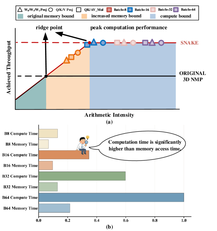
However, in the 3D NMP setting, many decode tensor operators shift from being memory-bound back to compute-bound. Since decode performance remains primarily dominated by tensor operators, we focus our analysis on matrix multiplication and its associated memory-access behavior from a roofline perspective. As shown in Figure 1 (a), existing 3D NMP architectures have not scaled on-stack compute capability commensurately with the rapid growth in internal memory bandwidth. Taking Duplex (Yun et al., 2024) and Stratum (Pan et al., 2025) as representative 3D-stacked NMP architectures, their compute-to-memory-bandwidth ratio only reaches 8 and 3.7–6.7 FLOPs/Byte, respectively, while decode operators are often required to support batch sizes of up to 64 in practical serving (Pan et al., 2025; Li et al., 2026), resulting in arithmetic intensity that frequently and significantly exceeds these hardware ridge points. As corroborating evidence in Figure 1 (b), our reproduction of Stratum (Pan et al., 2025), conducted on LLaMA3 models across varying batch sizes, shows that, even with double buffering to overlap data movement with execution, array compute time remains substantially longer than memory-supply time, indicating that the currently provisioned compute throughput significantly lags behind the available memory supply capability.
Intrinsically, in heterogeneous LLM inference systems, the compute-bound behavior of 3D NMP arises from operator scheduling. Mainstream xPUs typically exhibit ridge points on the order of hundreds of FLOP/Byte or higher (Jouppi and Lakshmanamurthy, 2025; Choquette, 2023), making them naturally well suited for high–arithmetic-intensity prefill operators. Although techniques such as continuous batching and attention variants (e.g., GQA/MQA) can increase arithmetic intensity, decode operators still remain far below prefill workloads. Therefore, in heterogeneous systems, decode operators are preferentially assigned to 3D-stacked NMP, where even many medium-to-low arithmetic-intensity decode operators become compute-bound thanks to the high local memory bandwidth.
<details>
<summary>2604.04253v2/x1.png Details</summary>
### Visual Description
## Line Graph with Bar Chart: Achieved Throughput vs Arithmetic Intensity and Compute/Memory Time Breakdown
### Overview
The image contains two primary components:
1. A **line graph** (a) showing the relationship between arithmetic intensity and achieved throughput, with regions demarcating memory/compute bounds and batch size configurations.
2. A **bar chart** (b) comparing compute and memory access times across different batch sizes (B8, B16, B32, B64).
---
### Components/Axes
#### Line Graph (a)
- **X-axis**: "Arithmetic Intensity" (no explicit scale, but labeled with "ridge point" and "peak computation performance").
- **Y-axis**: "Achieved Throughput" (units unspecified, but normalized to a 0–1 scale).
- **Legend**:
- Symbols:
- Triangles (▲): W0/W1/W2 Proj
- Circles (●): Q/K/V Proj
- Squares (■): QK/AV_Mul
- Filled squares (■): Batch=8 (red), Batch=16 (blue), Batch=32 (pink), Batch=64 (purple)
- Colors:
- Green: Original memory bound
- Orange: Increased memory bound
- Blue: Compute bound
- **Key Markers**:
- Red dashed line labeled "SNAKE" (horizontal, spans high arithmetic intensity).
- Black dashed line labeled "ORIGINAL 3D NMP" (horizontal, baseline throughput).
- Arrows labeled "ridge point" (intersection of original memory bound and increased memory bound) and "peak computation performance" (transition to compute bound).
#### Bar Chart (b)
- **X-axis**: Normalized time (0.0–1.0, no units).
- **Y-axis**: Batch sizes and time categories:
- B8 Compute Time
- B8 Memory Time
- B16 Compute Time
- B16 Memory Time
- B32 Compute Time
- B32 Memory Time
- B64 Compute Time
- B64 Memory Time
- **Colors**:
- Orange: Compute Time
- Green: Memory Time
---
### Detailed Analysis
#### Line Graph (a)
- **Trends**:
- Throughput increases linearly with arithmetic intensity until the "ridge point" (~0.3 arithmetic intensity), after which it plateaus.
- The "peak computation performance" occurs at the transition to the blue "compute bound" region (~0.5 arithmetic intensity).
- Batch sizes (B8–B64) are plotted as points along the curve, with larger batches (B64) achieving higher throughput.
- **Data Points**:
- Ridge point: ~0.3 arithmetic intensity, ~0.45 throughput.
- Peak computation performance: ~0.5 arithmetic intensity, ~0.7 throughput.
- SNAKE line: Horizontal at ~0.7 throughput, spanning high arithmetic intensity.
#### Bar Chart (b)
- **Values** (approximate):
- **B8**:
- Compute Time: ~0.15
- Memory Time: ~0.08
- **B16**:
- Compute Time: ~0.35
- Memory Time: ~0.12
- **B32**:
- Compute Time: ~0.60
- Memory Time: ~0.18
- **B64**:
- Compute Time: ~1.00
- Memory Time: ~0.22
- **Speech Bubble**: "Computation time is significantly higher than memory access time" (emphasizes compute dominance).
---
### Key Observations
1. **Memory vs. Compute Bound**:
- Below the ridge point, memory access limits throughput (green/orange regions).
- Beyond the ridge point, compute becomes the bottleneck (blue region).
2. **Batch Size Impact**:
- Larger batches (B64) achieve higher throughput but require more compute resources.
- Memory time remains relatively constant across batches, while compute time scales linearly.
3. **SNAKE Line**:
- Represents an optimal throughput threshold (~0.7) achievable at high arithmetic intensity.
---
### Interpretation
- **Performance Bottlenecks**:
- At low arithmetic intensity, memory access (W0/W1/W2, Q/K/V projections) dominates.
- At high arithmetic intensity, compute resources (QK/AV_Mul) become critical.
- **Batch Size Tradeoffs**:
- Larger batches improve throughput but increase compute time disproportionately (e.g., B64 compute time = 1.0 vs. B8 = 0.15).
- **SNAKE Line Significance**:
- Likely represents a target or theoretical maximum throughput achievable under ideal conditions.
- **Original 3D NMP Baseline**:
- The black dashed line indicates the original model’s performance, which is surpassed by optimized configurations (e.g., B64).
The data suggests that optimizing for compute-bound scenarios (via larger batches and efficient memory projections) is critical for maximizing throughput in arithmetic-intensive workloads. The "SNAKE" line may indicate a design goal or upper limit for system performance.
</details>
Figure 1. (a) Roofline Analysis of LLM Decode Operators on 3D-Stacked NMP (b) Memory-Side Execution Analysis of Decode Operators in Stratum Limitations of existing 3D-stacked NMP architectures for LLM decoding. Despite high internal memory bandwidth, both Duplex and Stratum remain compute-limited, resulting in under-utilized memory bandwidth and limited latency hiding.
One of the fundamental limitations is the severely constrained area available to the NMP engine on the logic die. In practice, only a limited fraction of the logic die can be allocated to active compute logic. Stratum is a representative example: to maintain compatibility with the HBM3 xPU–DRAM interface, the logic die must reserve substantial area for the HBM3 PHY, DRAM peripherals, and power-delivery overhead, which significantly compresses the area budget available for active logic. Then, HBM logic dies remain physically compact—e.g., around 121 mm² in HBM3-class designs—because their footprint is constrained by advanced-package assembly and reliability requirements, a tight thermal envelope, and poor cost efficiency under die-area scaling (Kim and Park, 2024; Moon et al., 2023; Lau, 2022). As a result, Stratum reports an active logic area of only about 76.63 mm². In contrast, the neighboring xPU typically exposes only a fraction of the memory bandwidth available on the NMP side, yet can devote an effective compute area that is an order of magnitude larger.
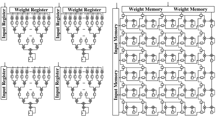
Therefore, 3D-stacked NMP requires a different compute substrate design point: one that maximizes compute density under a severely constrained logic-die area budget. From the perspective of compute unit, MAC-Tree-based designs have been widely adopted in prior work (Pan et al., 2025; Yun et al., 2024; Huang et al., 2025; Li et al., 2025) as a mainstream solution. However, as their scale increases, the high-fanout operand buffer delivery paths and multi-stage reduction networks tend to incur substantial interconnect and control overhead, ultimately limiting area efficiency and scalability (detailed in Section 2). In contrast, Systolic Array (SA) organizes a large number of simple processing elements, each performing only basic multiply–accumulate operations, into a two-dimensional structure connected through regular nearest-neighbor links. By exploiting structured data movement, it enables high compute density and array-level data reuse within the fabric, and therefore typically offers superior area efficiency and energy efficiency. This makes it a more suitable compute substrate for area-constrained 3D NMP architectures. This architectural advantage is also borne out by our RTL implementations: under the same frequency and PE-level compute functionality, the MAC-Tree design requires 8.23× more area than SA.
However, directly adopting a conventional SA for LLM decode on 3D-stacked NMP is not straightforward. A closer examination of this setting reveals two key requirements. Operators mapped to a single core during decode exhibit substantial shape diversity, making it difficult for a fixed-shape array to sustain high utilization, especially when many of these operators have already become compute-bound. Moreover, the dimensional relationships among operators can also change the preferred systolic dataflow. A decode-oriented SA therefore must support reconfigurability in both array shape and dataflow.
Beyond the intrinsic area efficiency of SA, the 3D-stacked NMP setting also creates two architectural opportunities to further improve compute-area efficiency and thereby deploy more compute to alleviate bottlenecks. On the one hand, higher local memory bandwidth weakens the conventional need for large-capacity buffers, making it possible to increase the number of compute units by reducing buffer area. On the other hand, the auxiliary vector core already provides fine-grained control and flexible buffering, offering a useful foundation for exploring a unified systolic-vector compute substrate, and thus may enable the required reconfigurability at lower area overhead.
Based on these insights, we propose SNAKE, a reconfigurable SA tailored for LLM decode on 3D-stacked NMP, together with a co-designed multi-core scheduling framework. More broadly, architecture research has rarely studied multi-core scheduling for reconfigurable SA in a systematic way. We address this gap by exploring this scheduling space and applying it to high-bandwidth 3D-stacked NMP. The main contributions are as follows:
- We identify the compute-area bottleneck of LLM decode on current 3D-stacked NMP and derive from it the need for reconfigurable systolic execution in both array shape and dataflow, together with two architectural opportunities that enable the required flexibility while freeing area for additional compute units.
- We propose SNAKE, a reconfigurable SA whose microarchitecture is optimized for 3D-stacked NMP, meeting the key requirements of LLM decode: high bandwidth utilization, low area overhead, and fine-grained reconfigurability. To achieve this, we introduce a systolic–vector architecture combined with SNAKE-like mapping for area efficiency and high utilization.
- We introduce a multi-core scheduling framework, enabled by a lightweight on-chip interconnect, that efficiently exploits the abundant array resources and high local bandwidth of 3D-stacked NMP by aligning systolic dataflows with spatial and spatio-temporal partitioning.
- Compared with state-of-the-art 3D NMP baseline, SNAKE achieves 4.00× higher compute-area efficiency, and delivers an average 2.90× speedup and 2.40× higher energy efficiency across diverse LLMs.
## 2. BACKGROUND AND DESIGN CONTEXT
MAC Tree and Systolic Array
<details>
<summary>2604.04253v2/x2.png Details</summary>
### Visual Description
## Diagram: Computational Architecture with Input/Weight Registers and Memory
### Overview
The diagram illustrates a hierarchical computational architecture composed of four identical left-side structures labeled "Input Register" and "Weight Register," and a large right-side grid labeled "Weight Memory." The left structures feature a vertical flow of interconnected components, while the right grid shows a matrix of blocks with symbolic operations.
### Components/Axes
- **Left Structures (4x)**:
- **Labels**:
- Top: "Weight Register" (repeated twice per structure)
- Bottom: "Input Register" (repeated twice per structure)
- **Components**:
- Pyramid-like hierarchy of interconnected nodes (circles with "+" and "×" symbols).
- Vertical flow from "Input Register" (bottom) to "Weight Register" (top).
- **Flow Direction**: Bottom-to-top processing.
- **Right Grid**:
- **Labels**:
- Top: "Weight Memory" (repeated twice horizontally)
- Left: "Input Memory" (vertical label)
- **Components**:
- 4x4 grid of square blocks (16 total).
- Each block contains a "+" (top-left) and "×" (bottom-right) symbol.
- Connections between blocks form a dense network.
### Detailed Analysis
- **Left Structures**:
- Each "Input Register" feeds into a tiered system of nodes, culminating in two "Weight Register" blocks at the top.
- Symbols ("+" and "×") suggest arithmetic operations (addition/subtraction) within the hierarchy.
- Repetition of structures implies parallel processing units.
- **Right Grid**:
- "Input Memory" vertically feeds into the grid, with horizontal connections between "Weight Memory" blocks.
- Each block’s "+" and "×" symbols indicate localized operations, possibly for weight updates or data aggregation.
- Grid layout suggests distributed memory storage or parallel computation.
### Key Observations
1. **Hierarchical vs. Distributed Processing**:
- Left structures emphasize vertical, layered computation.
- Right grid emphasizes horizontal, parallelized memory operations.
2. **Symbol Consistency**:
- "+" and "×" symbols are uniformly distributed, implying standardized operations across the architecture.
3. **Modularity**:
- Left structures are identical, suggesting reusable processing modules.
- Right grid’s uniformity indicates scalable memory management.
### Interpretation
This diagram likely represents a neural network or machine learning accelerator architecture. The left structures model **input processing layers** where data is transformed through arithmetic operations before being stored in **weight registers**. The right grid represents **weight memory**, where computed values are aggregated and updated in parallel. The "+" and "×" symbols highlight the role of linear algebra (e.g., matrix multiplication) in the system. The separation of input processing (left) and memory storage (right) suggests an optimized pipeline for high-throughput computation, common in hardware accelerators for AI workloads.
</details>
Figure 2. Microarchitectural Comparison of MAC Tree and Systolic Array Limitations of SAs for Non-Linear and Reduction Operations
SA and MAC-Tree architectures take different approaches to multiply-accumulate (MAC) computation. An SA is a 2D grid of simple processing elements (PEs), each performing only MACs and communicating via nearest-neighbor links. Inputs and weights are fed from array-edge buffers and propagate in a regular pattern, enabling high compute density and efficient data reuse. This simplicity makes SAs area- and energy-efficient for dense, regular matrix workloads.
By contrast, MAC Trees place greater emphasis on organizing computation around parallel multipliers and a hierarchical reduction network. As illustrated in Figure 2, a MAC-Tree structure feeds a set of parallel multipliers from the weight registers at the top and the input registers on the left, and then progressively reduces the multiplier outputs through a multi-level adder tree to produce the final result. Unlike the regular nearest-neighbor dataflow in SA, this type of architecture incorporates both a high-fanout operand-delivery path and a hierarchical reduction path: the former distributes inputs and weights to multiple multipliers, while the latter incrementally merges multiple product terms across reduction stages. As parallelism increases, the implementation complexity of these two structures in physical layout and timing closure typically grows further, which can limit area efficiency at large scale. From an energy-efficiency perspective, MAC Trees usually require stronger vector broadcast and reduction networks, leading to higher on-chip data-movement energy. Moreover, under batched GEMM workloads, they are less able to exploit array-level data reuse, further degrading energy efficiency.
However, SA’s utilization can drop substantially when the workload exhibits the following characteristic. This is a well-known classical challenge, and a large body of prior work has explored this issue (Samajdar et al., 2022; Han et al., 2024; Lee et al., 2021; Ghodrati et al., 2020). Among them, prior work has also explored integrating SA with more flexible compute engines, such as CPU (Ju and Gu, 2022; Jeong et al., 2021), GPU (Guo et al., 2020), or vector-style processing units (Maceiras et al., 2022), to better handle irregular workloads for specific hardware scenarios. Prior flexible SA designs mainly target general shape-diverse DNN workloads, improving utilization through fine-grained reshaping and multiple dataflows at the single-array level. In contrast, SNAKE focuses on the more structured workload space of popular multi-batch LLM decode, and accordingly adopts a more targeted form of reconfigurability in array shape and dataflow. Moreover, prior work largely remains at the single-array or single-core level, whereas SNAKE further studies how such reconfigurable systolic execution should be orchestrated across multiple cores and across operators in the LLM decode setting.
We further identify 3D-stacked NMP as the natural deployment setting for reconfigurable SA for LLM decode: in lower-bandwidth platforms, decode remains memory-bound, so utilization improvements yield limited benefit, whereas the high local bandwidth of 3D-stacked NMP both makes such gains effective and enables buffer-to-compute area reallocation.
3D-Stacked Accelerators To address the high bandwidth demand of LLM inference, the accelerators have evolved from bank-level in-DRAM processing designs (Heo et al., 2024; Park et al., 2024; Lee et al., 2022) to NMP providing higher compute capability in the logic die (Yun et al., 2024). Stratum (Pan et al., 2025) further introduces the co-design of the 3D DRAM organization and expert activation characteristics in MoE. Prior work mainly adopts MAC-Tree-based architectures, and the available compute capability remains mismatched with the memory bandwidth, while paying limited attention to the MNK-level shape characteristics.
Although recent works lean toward directly integrating larger compute arrays to study thermal behavior (He et al., 2025) and attention-centric LLM serving design deployment (Li et al., 2026), they assume a logic-die area that is difficult to reconcile with realistic HBM3-class, and even near-term HBM4-class, packages, without sufficient justification for its manufacturing and packaging feasibility. As a result, some of their conclusions do not directly apply to our setting. For example, Tasa studies thermal behavior under many-core scaling, whereas our work focuses on improving compute-area efficiency under a fixed logic-die area budget. SK Hynix (Han et al., 2025) attempts to deploy one SA under normal area budget, but they target both prefill and decode simultaneously. This work advocates a heterogeneous architecture that couples conventional XPUs with 3D-stacked NMP, where compute-intensive prefill is handled by resource-rich XPUs, while memory-dominated decode is offloaded to area-constrained NMP logic dies to better exploit their high local bandwidth.
In contrast to prior work, which primarily optimizes 3D-stacked inference from the perspectives of DRAM organization (Pan et al., 2025; Yun et al., 2024) and operator mapping (Li et al., 2025, 2026; Huang et al., 2025), this work rethinks the compute microarchitecture under the stringent area constraints of the logic die. As such, it is largely orthogonal to existing 3D-stacked memory optimizations and can be combined with them.
## 3. KEY OBSERVATIONS
### 3.1. Motivation: The Need for Reconfigurability
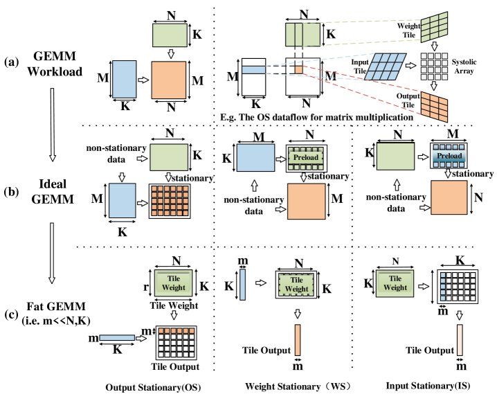
To unify LLM linear operators, we abstract them as GEMM $A× B=C$ , where $A∈ℝ^M× K$ , $B∈ℝ^K× N$ , and $C∈ℝ^M× N$ . In a 2D SA, two of $\{M,N,K\}$ are mapped to the array’s two spatial dimensions, while the remaining one is unfolded temporally. As illustrated in Figure 3 (b), output-stationary (OS) maps $M$ and $N$ spatially and unfolds $K$ over time, whereas IS maps $M$ and $K$ spatially and unfolds $N$ .
Since practical GEMMs usually exceed a single array’s capacity, they must be tiled and executed across multiple rounds. As illustrated in Figure 3 (a), dimensions mapped to the array rows or columns require spatial tiling when they exceed array capacity, while the temporal dimension may also be segmented into multiple phases when it is too long for continuous buffered execution. For example, under OS, oversized $M$ or $N$ leads to spatial tiling, whereas oversized $K$ is split temporally. These spatial and temporal tiles, together with the fat-GEMM pattern in Figure 3 (c), form the basic units for later parallel scheduling across multiple cores.
<details>
<summary>2604.04253v2/x3.png Details</summary>
### Visual Description
## Diagram: GEMM Workload and Optimization Strategies
### Overview
The diagram illustrates three GEMM (General Matrix Multiply) workload configurations: (a) Standard GEMM Workload, (b) Ideal GEMM, and (c) Fat GEMM. It emphasizes dataflow optimization, memory access patterns, and tile-based computation strategies. Key components include matrix dimensions (M, N, K), stationary/non-stationary data, and systolic array operations.
### Components/Axes
- **Labels**:
- **Section (a)**: GEMM Workload, M, N, K, Input Tile, Weight Tile, Systolic Array, Output Tile.
- **Section (b)**: Ideal GEMM, non-stationary data, stationary data, Tile Weight, Preload, Tile Output.
- **Section (c)**: Fat GEMM (m < N, K), Tile Weight, Tile Output, Output Stationary (OS), Weight Stationary (WS), Input Stationary (IS).
- **Colors**:
- Green: Non-stationary data/Weight Tile.
- Blue: Stationary data/Input Tile.
- Orange: Output Tile/Stationary data.
- Red: Dashed lines indicating dataflow paths.
- **Flow Direction**:
- Left-to-right for dataflow (e.g., Input Tile → Weight Tile → Systolic Array → Output Tile).
- Vertical arrows denote stationary/non-stationary data separation.
### Detailed Analysis
1. **Section (a): GEMM Workload**
- Matrices M (blue), N (green), and K (orange) are multiplied via a systolic array.
- Non-stationary data (green) flows into the systolic array, while stationary data (orange) is preloaded.
- Output Tile (orange) is generated after matrix multiplication.
2. **Section (b): Ideal GEMM**
- Separates data into non-stationary (green) and stationary (blue/orange) streams.
- Non-stationary data is tiled into Weight Tiles (green), while stationary data is preloaded into the systolic array.
- Tile Output (orange) is produced after processing.
3. **Section (c): Fat GEMM (m < N, K)**
- Smaller tile size (m) reduces memory bandwidth.
- Three stationary types:
- **Output Stationary (OS)**: Processes Tile Output (orange) with dimensions m×K.
- **Weight Stationary (WS)**: Handles Tile Weight (green) with dimensions K×m.
- **Input Stationary (IS)**: Manages Input Tile (blue) with dimensions N×m.
### Key Observations
- **Dataflow Optimization**:
- Ideal GEMM reduces non-stationary data movement by tiling weights and preloading stationary data.
- Fat GEMM minimizes tile size (m) to balance compute and memory constraints.
- **Systolic Array Role**:
- Central to matrix multiplication in all configurations, enabling parallel computation.
- **Tile Size Tradeoffs**:
- Fat GEMM’s smaller tiles (m) may improve cache efficiency but increase tile count.
### Interpretation
The diagram highlights strategies to optimize GEMM operations for hardware efficiency:
1. **Ideal GEMM** balances non-stationary and stationary data to minimize memory access latency.
2. **Fat GEMM** adapts to memory bandwidth limitations by reducing tile dimensions, critical for large matrices (M, N, K).
3. **Systolic Array** acts as a computational engine, with dataflow paths (red dashed lines) emphasizing parallelism.
The progression from (a) to (c) suggests a tradeoff between computational complexity and memory efficiency, with Fat GEMM prioritizing memory constraints over tile size. This aligns with hardware-aware algorithm design for deep learning accelerators.
</details>
Figure 3. GEMM Abstraction and Systolic Dataflows GEMM Abstraction and Systolic Dataflows
The LLM decode workloads in Figure 3 (c) impose two requirements on SA reconfigurability of shape and dataflow:
First, this workload characteristic motivates array-shape reconfigurability. Decode operators are generally characterized by $M\ll N,K$ , and further partitioning the already small $M$ dimension across cores is undesirable because it would incur large-weight replication with significant communication overhead (Yun et al., 2024; Pan et al., 2025). As a result, the per-core workload usually preserves the original $M$ dimension, which itself remains dynamic across batch sizes and attention configurations, e.g., GQA or MLA. The resulting single-core decode tiles still typically satisfy $N,K\gg M$ .
Conventional SA usually adopt a near-square shape for generality, since such organizations can better accommodate diverse GEMM shapes. Conventional SA also tend to employ relatively large arrays, since larger arrays usually offer higher data reuse and better area efficiency than smaller ones. Therefore, in decode the mapped $M$ dimension is often smaller than the array dimension assigned to it, leaving many PEs idle across operators and requests. Under 3D-stacked NMP, where abundant local bandwidth often shifts decode into the compute-bound regime, this utilization loss can directly translate into higher latency, while also weakening data reuse and energy efficiency.
Second, this workload characteristic also motivates dataflow reconfigurability. Since single-core decode tiles also typically satisfy $N,K\gg M$ , it is sufficient to consider only OS and input-stationary (IS) while excluding weight-stationary (WS). As shown in Figure 3 (c), a suitable dataflow should place one of the two large dimensions, $N$ or $K$ , on the temporal dimension, so that each tile sustains longer execution, better amortizes data-loading and startup overheads, and reduce tile switching. By contrast, WS relies more on the much smaller $M$ dimension and is therefore less suitable for decode.
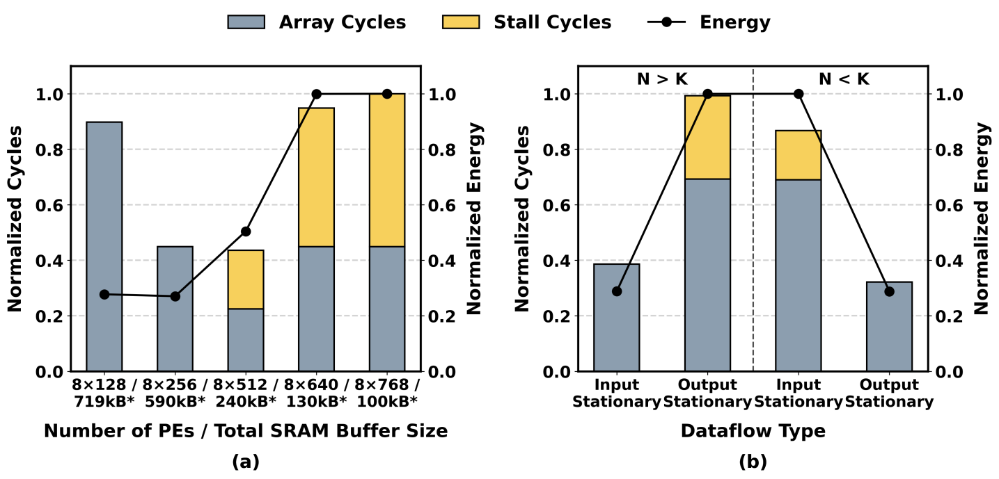
Accordingly, IS is generally preferable when $N>K$ , because making $N$ temporal reduces repeated re-tiling and rereading along $N$ ; conversely, when $K≥ N$ , OS is more favorable because it unfolds $K$ temporally. To validate this first-order trend, we profile all operators of OPT 66B decode under the decode configuration detailed in Table 1, at batch size 8, and separately extract the single-core tiled workloads with $N>K$ and with $N≤ K$ . As shown in Figure 4 (b), the two groups exhibit different preferred dataflows on average, while the final best choice can still vary with runtime conditions because dataflow choice affects both array cycles and memory-side stall cycles. Here, stall cycles arise when double-buffered tile refills cannot keep pace with array consumption due to insufficient effective refill bandwidth.
### 3.2. Opportunity 1: High Local Bandwidth Enables Buffer-to-Compute Reallocation.
In conventional SA constrained by off-chip bandwidth, on-chip SRAM buffers are typically large for two reasons. First, they support double buffering, so that one region supplies the current tile while another prefetches the next tile to hide memory latency. Second, they keep inputs, weights, and partial sums on chip for reuse. As a result, buffering occupies a large fraction of area. By contrast, each PE implements only simple MAC logic and is much smaller than large SRAM arrays.
<details>
<summary>2604.04253v2/x4.png Details</summary>
### Visual Description
## Bar Charts with Line Plot: Performance Metrics Across Configurations
### Overview
The image contains two bar charts (labeled a and b) with overlaid line plots, comparing normalized cycles and energy metrics across different hardware configurations and dataflow scenarios. The charts use color-coded bars (gray for "Array Cycles," orange for "Stall Cycles") and a black line with markers for "Energy." Both charts emphasize trade-offs between computational efficiency and energy consumption.
---
### Components/Axes
#### Chart (a): PE/Buffer Size vs. Performance
- **X-axis**:
- Categories: "8x128 / 719kB*", "8x256 / 590kB*", "8x512 / 240kB*", "8x640 / 130kB*", "8x768 / 100kB*"
- Labels represent combinations of Processing Elements (PEs) and total SRAM buffer sizes.
- **Y-axis**:
- "Normalized Cycles" (left scale, 0.0–1.0)
- "Normalized Energy" (right scale, 0.0–1.0)
- **Legend**:
- Gray: "Array Cycles"
- Orange: "Stall Cycles"
- Black line with dots: "Energy"
- **Line Plot**:
- Connects energy data points across configurations.
#### Chart (b): Dataflow Type vs. Performance
- **X-axis**:
- Categories: "Input Stationary," "Output Stationary," "Input Stationary," "Output Stationary" (repeated labels suggest a possible error or intentional grouping).
- Vertical dashed line separates "N > K" (left) and "N < K" (right).
- **Y-axis**:
- Same as Chart (a): "Normalized Cycles" and "Normalized Energy."
- **Legend**:
- Same as Chart (a): Gray ("Array Cycles"), Orange ("Stall Cycles"), Black line ("Energy").
---
### Detailed Analysis
#### Chart (a) Trends
1. **Array Cycles (Gray Bars)**:
- Decrease monotonically as PEs/buffer size increases (e.g., 8x128: ~0.9, 8x768: ~0.45).
- Suggests higher parallelism reduces per-cycle workload.
2. **Stall Cycles (Orange Bars)**:
- Increase with larger configurations (e.g., 8x128: ~0.1, 8x768: ~0.55).
- Indicates growing overhead (e.g., memory contention, synchronization).
3. **Energy (Black Line)**:
- Peaks at 8x640 and 8x768 (~0.95), then plateaus.
- Energy efficiency worsens with larger configurations despite lower array cycles.
#### Chart (b) Trends
1. **N > K (Left Side)**:
- **Input Stationary**: Array cycles ~0.7, Stall cycles ~0.3.
- **Output Stationary**: Array cycles ~0.7, Stall cycles ~0.3.
- Energy peaks at ~0.95 for both input/output.
2. **N < K (Right Side)**:
- **Input Stationary**: Array cycles ~0.4, Stall cycles ~0.4.
- **Output Stationary**: Array cycles ~0.4, Stall cycles ~0.4.
- Energy drops to ~0.35, showing improved efficiency.
---
### Key Observations
1. **Trade-off in Chart (a)**:
- Larger PEs/buffer sizes reduce array cycles but increase stall cycles, with energy peaking at mid-to-high configurations.
2. **Dataflow Sensitivity in Chart (b)**:
- "N > K" and "N < K" scenarios show divergent performance:
- **N > K**: Higher array cycles but lower stall cycles (better for compute-bound tasks).
- **N < K**: Balanced array/stall cycles but lower energy (better for memory-bound tasks).
3. **Energy Anomaly**:
- Energy peaks at 8x640/8x768 in Chart (a) despite lower array cycles, suggesting hidden overheads (e.g., memory access latency).
---
### Interpretation
The data highlights a critical tension between computational efficiency and energy consumption:
- **Chart (a)** demonstrates that increasing parallelism (PEs/buffer) improves array cycle efficiency but introduces diminishing returns due to stall cycles and energy spikes. This suggests architectural limits to scaling.
- **Chart (b)** reveals that dataflow type (input/output) and the N/K relationship dictate performance:
- **N > K**: Favors compute-heavy workloads with higher array utilization but risks energy waste.
- **N < K**: Optimizes for memory-bound tasks with balanced cycles and lower energy, ideal for latency-sensitive applications.
- **Practical Implication**: System designers must balance PE count, buffer size, and dataflow patterns to avoid energy inefficiencies while maintaining throughput. The repeated "Input Stationary" labels in Chart (b) may indicate a data labeling error, warranting verification.
</details>
Figure 4. Impact of Buffer Allocation and Dataflow Choice on Decode Execution Impact of Buffer Allocation and Dataflow Choice on Decode Execution
Under NMP, the high local bandwidth of 3D-stacked memory and the lower cost of data movement weaken these conventional reasons for large buffers. Meanwhile, as discussed earlier, decode becomes more likely to be limited by effective compute supply. To examine this opportunity, we also use OPT 66B (batch = 8), as a representative decode workload. We allocate most of the SRAM budget to the weight buffer and keep the input and output buffers small. We then keep the total area budget fixed, gradually reduce SRAM capacity, and use the reclaimed area to increase the number of PEs, thereby exploring a buffer–compute reallocation space.
Figure 4 (a) shows the trade-off. As the PE count increases from 8 $×$ 128 to 8 $×$ 512, array cycles drop significantly, showing that the benefit of extra compute outweighs the loss of buffer capacity. However, when the configuration is further scaled to 8 $×$ 640 and 8 $×$ 768, stall cycles and energy rise sharply, indicating that the buffer has become too small to sustain efficient data supply, and the array dimensions also introduce unfavorable tile mismatch. We therefore choose an elongated 8 $×$ 512 physical organization as the PE configuration. As shown later in Section 6.6, batch size 8 corresponds to the highest weight-buffer demand and therefore represents the most conservative point in our analysis, while the benefit of provisioning more compute becomes more pronounced at higher batch sizes.
This result highlights two effects. First, for compute-bound decode operators, more compute units relieve the bottleneck more effectively, and the larger array can also reduce tile folds, lowering both compute and memory latency. Second, under high-bandwidth NMP, data staging and prefetching complete much faster, so large double-buffered SRAMs are less necessary. Even when a smaller buffer occasionally causes extra DRAM accesses, the penalty is much lower than in conventional off-chip-bandwidth-limited platforms. Prior work reported a similar trend. TETRIS (Gao et al., 2017) targets CNN/FC inference and uses an Eyeriss-based (Chen et al., 2016) accelerator in each 3D-memory vault to shift area from the global buffer to more PEs. Our work instead targets shape-diverse LLM decode and uses the reclaimed area not just for more fixed compute, but for a reconfigurable systolic substrate that adapts both array shape and dataflow to the workload.
### 3.3. Opportunity 2: Unifying Vector-Style Flexibility with Systolic Efficiency.
<details>
<summary>2604.04253v2/x5.png Details</summary>
### Visual Description
## Diagram: 3D HBM and TPU/GPU System Architecture
### Overview
The diagram illustrates a complex 3D heterogeneous computing system integrating 3D High Bandwidth Memory (HBM), TPU/GPU, compute tiles, logic dies, and interposers. It includes detailed views of memory hierarchy (cache, buffer), processing units (SIMD Unit/VPU), and optimization metrics. The system emphasizes hybrid bonding/through-silicon vias (TSVs) for interconnectivity.
### Components/Axes
1. **3D HBM**:
- Labeled as "3D HBM" with stacked layers.
- Arrows indicate data flow (downward from HBM to lower layers).
- Detail view shows "DRAM Dies" with "Hybrid Bonding/Through-Silicon Vias (TSVs)."
2. **TPU/GPU**:
- Labeled "TPU/GPU" as a large blue block.
- Connected to the interposer via dashed lines.
3. **Compute Tiles**:
- Labeled "Compute Tiles" with green blocks.
- Arrows point to "Logic Die" (smaller green block).
4. **Interposer**:
- Central orange block labeled "Interposer."
- Connects "Logic Die" to "TPU/GPU."
5. **SIMD Unit (VPU)**:
- Grid of white/blue squares labeled "SIMD Unit (VPU)."
- Connected to "Cache" (vertical blue bar) and "Buffer" (vertical blue bar).
6. **VRF**:
- Horizontal orange block labeled "VRF" below the SIMD Unit.
7. **Optimization Metrics**:
- Gauge labeled "SA Utilization Status: Poor" (red needle).
- List of "Non-Linear Functions": Softmax, Sigmoid, ReLU, GeLU, Activation Function, Hadamard Product, SiLU.
### Detailed Analysis
- **3D HBM**:
- Multiple layers (4–5) with data flowing downward via TSVs.
- Detail view confirms TSVs as vertical interconnects between DRAM dies.
- **TPU/GPU**:
- Positioned as the primary processing unit, connected to the interposer.
- **Compute Tiles & Logic Die**:
- Compute Tiles (green) and Logic Die (smaller green) are part of the lower layer, feeding data to the interposer.
- **SIMD Unit (VPU)**:
- Grid structure suggests parallel processing units.
- Connected to cache and buffer for data storage/retrieval.
- **VRF**:
- Positioned below the SIMD Unit, possibly for voltage/frequency control.
- **Optimization Metrics**:
- Gauge indicates "Poor" utilization, suggesting inefficiency in system performance.
- Non-linear functions are standard in neural networks, implying the system is optimized for AI/ML workloads.
### Key Observations
- **Data Flow**: Data moves from 3D HBM through the interposer to the TPU/GPU, with intermediate processing in compute tiles and logic dies.
- **Poor Utilization**: The "Poor" SA utilization metric highlights potential bottlenecks or underutilization of resources.
- **Non-Linear Functions**: The presence of activation functions (e.g., ReLU, GeLU) confirms the system’s use in deep learning.
### Interpretation
The diagram represents a high-performance computing architecture optimized for AI/ML tasks. The 3D HBM provides high-bandwidth memory access, while the TPU/GPU handles parallel computations. The interposer and TSVs enable efficient interconnectivity between layers. However, the "Poor" SA utilization suggests inefficiencies, possibly due to suboptimal workload distribution or hardware limitations. The inclusion of non-linear functions underscores the system’s focus on neural network acceleration. The VRF and cache/buffer components indicate a focus on power management and data throughput optimization. Overall, the architecture balances memory, processing, and optimization, but the poor utilization metric warrants further investigation into system design or workload management.
</details>
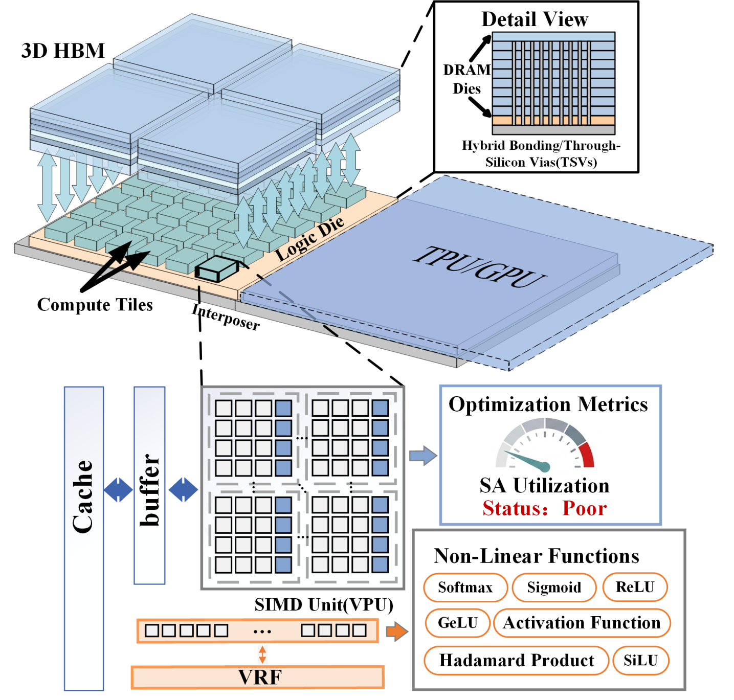
Figure 5. Vector and Systolic Core Compute Substrate for 3D-Stacked NMP. Overview of a 3D-stacked NMP system architecture.
Existing 3D NMP designs follow different architectural paths (Pan et al., 2025; Li et al., 2026; He et al., 2025), but they ultimately require two classes of capability at the same time. As shown in Figure 5, the first is high-density computation for tensor MAC operations. The second is flexible execution support for nonlinear operators, reductions, element-wise processing, and fine-grained control. The former aligns naturally with systolic execution, whereas the latter is more closely associated with vector-style execution.
In 3D-stacked NMP, the area budget on the logic die is extremely constrained. Our earlier analysis shows that decode workloads require not only high-density MAC capability, but also flexibility to accommodate dynamic variation in array shape and dataflow. This suggests that a more promising direction is not to mechanically place a vector core beside a SA, but rather to build a unified compute substrate that reuses vector-side control, buffering, and reduction support to provide vector-style flexibility together with systolic-style efficiency.
## 4. ARCHITECTURE
<details>
<summary>2604.04253v2/x6.png Details</summary>
### Visual Description
## Block Diagram: Computing Architecture for Processing Elements (PEs) and Memory Interface
### Overview
The diagram illustrates a modular computing architecture featuring a 4x4 array of Processing Elements (PEs) organized into four SRAM regions (Top, Bottom, Left, Right). The system includes a memory interface with a load/store unit, controller, region table, and decoder. Data flows from a "Packet from Hotside" through the memory interface into the SRAMs, which are interconnected via crossbars to enable parallel processing. A vector controller and reduction unit are positioned at the bottom for data aggregation and control.
---
### Components/Axes
#### Labels and Structure:
1. **Memory Interface**:
- **Load/Store Unit**: Interface for memory operations.
- **Controller**: Manages data flow between memory and SRAMs.
- **Region Table**: Maps data regions to SRAM locations.
- **Decoder**: Processes incoming packets from the hotside.
- **Packet from Hotside**: Input data stream.
2. **SRAM Regions**:
- **TOP SRAM**: 4x4 grid of PEs (green).
- **BOTTOM SRAM**: 4x4 grid of PEs (green).
- **LEFT SRAM**: 4x4 grid of PEs (green).
- **RIGHT SRAM**: 4x4 grid of PEs (green).
3. **Processing Elements (PEs)**:
- 16 PEs arranged in a 4x4 grid (purple squares).
- Connected via **2x2 Crossbar** networks (blue lines) for horizontal and vertical data routing.
4. **Control and Processing Units**:
- **Vector Controller**: Manages vector operations (orange).
- **Reduction Unit**: Aggregates results (orange).
5. **Crossbar Connections**:
- Horizontal and vertical crossbars link PEs across all SRAM regions.
---
### Detailed Analysis
#### Memory Interface Workflow:
- Data enters via the **Load/Store Unit** and is managed by the **Controller**.
- The **Region Table** directs data to specific SRAM regions.
- The **Decoder** processes incoming packets from the hotside before routing to SRAMs.
#### SRAM and PE Organization:
- Each SRAM region (Top, Bottom, Left, Right) contains a 4x4 grid of PEs.
- Crossbars enable direct communication between PEs in adjacent regions (e.g., Top SRAM to Bottom SRAM via vertical crossbars).
#### Vector Controller and Reduction Unit:
- The **Vector Controller** coordinates vector operations across PEs.
- The **Reduction Unit** aggregates results (e.g., summing values) from PEs.
---
### Key Observations
1. **Modular Design**: SRAM regions and PEs are organized into distinct blocks for scalability.
2. **Crossbar Efficiency**: 2x2 crossbars minimize routing complexity while enabling full connectivity.
3. **Parallelism**: 16 PEs allow simultaneous computation, with crossbars facilitating inter-PE communication.
4. **Control-Centric Architecture**: The vector controller and reduction unit centralize data aggregation and task management.
---
### Interpretation
This architecture prioritizes **high-throughput parallel processing** with minimal latency. The crossbar interconnects eliminate the need for sequential data routing, enabling efficient communication between PEs. The modular SRAM regions suggest scalability for larger systems, while the vector controller and reduction unit indicate support for vectorized operations (e.g., matrix multiplications, common in machine learning). The "Packet from Hotside" implies integration with a data source (e.g., a GPU or accelerator), highlighting the system's role in high-performance computing tasks. The absence of explicit clock or power management components suggests a focus on computational efficiency over energy optimization in this design.
</details>
Figure 6. Architecture Overview. Architecture Overview.
### 4.1. Overview
Prior 3D NMP systems largely share a common stack-level template: logic-die-side compute engines are tightly coupled with stacked high-bandwidth memory. This work targets a different level of that design stack. Rather than redesigning the memory stack itself, we focus on the compute substrate on the logic die and develop an architecture that can be instantiated under similar stack-level assumptions, and the detailed reference setting is described in Section 6.1.2. The external xPU remains responsible for host-side coordination and complementary execution of operators from LLM prefill. In evaluation, we instantiate this organization using an HBM3 configuration consistent with prior 3D NMP studies.
At the logic-die level, we organize the stack into 16 processing units (PUs) connected by a lightweight NoC similar to Stratum (Pan et al., 2025), which is used only for coarse-grained communication such as all-reduce and all-gather. Each PU is bound to one memory channel and forms a locality-preserving compute-memory tile. Inside each PU, four compute cores are integrated. Each core is built around a 64×64 PE-based compute fabric together with local systolic buffering, while the detailed systolic-vector integration is described in Section 4.2. Like prior work (Yun et al., 2024; Pan et al., 2025), local channel access is preferred and fine-grained remote accesses are minimized. Within one PU, the four compute cores cooperatively execute the assigned local workload. To efficiently feed these cores, banks in the local channel are grouped into bank bundles for parallel tile refill. Data fetched from these bank bundles are first staged in the private systolic buffers, which provide lightweight layout reorganization and double-buffered tile supply before delivering tile-ready operand streams into the local SA.
### 4.2. Core Microarchitecture
Following the analysis in Section 3.3, we tightly integrate the vector core with the SA, so that the fine-grained execution substrate of the former can be reused to support fine-grained computation and reconfiguration in the latter.
#### 4.2.1. Array Design
As discussed above, our design already exploits the high local memory bandwidth of 3D-stacked NMP to reduce on-chip buffering and reallocate more area to PE arrays, thereby increasing compute density under the tight logic-die area budget. However, even after reducing the overall buffer footprint, the cost of reconfigurability itself remains a major concern. In a fine-grained reconfigurable SA, multi-ported buffers are still required to support sub-array reshaping and dataflow switching under different logical mappings, and prior work has shown that they are among the dominant area costs of such designs (Han et al., 2024). Therefore, the key objective of our array design is not only to shrink total buffer capacity, but also to further minimize the multi-port overhead needed for reconfiguration.
To make room for this capability, we reclaim part of the vector-side multi-ported buffering budget. In conventional Systolic Core + Vector Core LLM accelerators (Wu et al., 2025; Pan et al., 2025; He et al., 2025), the vector core typically relies on a heavily provisioned multi-ported local buffer to sustain reductions such as sum/max and element-wise post-processing at high standalone throughput. In our design, we do not preserve such a private buffer. Instead, we redirect part of that area to the SA side, where multi-port support more directly improves the utilization of small- $M$ decode operators mapped onto a large physical array. This trade-off is reasonable because vector-side nonlinear and reduction operators in LLM inference are typically small in scale and highly pipeline-friendly, so their latency can often be overlapped with preceding or subsequent GEMM execution (Pan et al., 2025). As described later, we further tighten this integration by allowing the SA and the vector core to share a common 2-read/2-write output buffer, similar to Gemmini (Genc et al., 2021), instead of maintaining separate multi-ported storage structures as in prior 3D-stacked NMP designs (Yun et al., 2024; Pan et al., 2025).
<details>
<summary>2604.04253v2/x7.png Details</summary>
### Visual Description
## Diagram: SRAM-Based Neural Network Layer Architecture
### Overview
The diagram illustrates a two-stage SRAM-based architecture for processing neural network layers, with two examples (Example1 and Example2) demonstrating different configurations. The system uses three SRAM banks (Top, Left, Right) and a Load-Balancing Unit to manage data flow. Colors represent data types: green (Input), blue (Weight), and orange (Output).
### Components/Axes
- **Legend**:
- Green: Input data
- Blue: Weight data
- Orange: Output data
- **Steps**:
1. Load Inputs into Top SRAM
2. Feed Inputs from Top SRAM into the Array
3. Load Weights into Left and Right SRAMs
4. Allocate Outputs to Bottom SRAM Banks via Load-Balancing Unit
- **Example Labels**:
- Example1: M=8 & Working in IS Mode
- Example2: M=16 & Working in IS Mode
- **Physical Size**: 64x64 (both examples)
- **Logical Sizes**:
- Example1: 8x512
- Example2: 16x256
### Detailed Analysis
- **Example1 (M=8)**:
- Logical size: 8 rows × 512 columns.
- SRAM configuration: Top SRAM feeds into an array of 64x64 processing elements (PEs), with weights distributed across Left/Right SRAMs.
- Outputs are routed to a bottom SRAM bank via the Load-Balancing Unit.
- **Example2 (M=16)**:
- Logical size: 16 rows × 256 columns.
- Similar SRAM structure but with doubled row count and halved column count compared to Example1.
- Increased parallelism in weight loading (visible in denser blue blocks).
### Key Observations
1. **Logical Size Tradeoff**:
- Example1 uses a narrower, deeper logical layout (8x512), while Example2 uses a wider, shallower layout (16x256).
- Both maintain the same physical SRAM size (64x64), suggesting logical partitioning.
2. **Weight Distribution**:
- Weights (blue) are split between Left and Right SRAMs, with Example2 showing more granular allocation.
3. **Load-Balancing Unit**:
- Outputs are dynamically routed to Bottom SRAM banks, implying adaptive resource management.
### Interpretation
- **Architectural Efficiency**:
- Example2’s higher M value (16 vs. 8) suggests improved parallelism for larger batch sizes or more complex operations, while Example1 may prioritize lower latency for smaller workloads.
- **IS Mode**:
- "IS Mode" likely refers to In-Situ processing, where computation occurs directly in SRAM to reduce data movement overhead.
- **Load-Balancing Role**:
- The Load-Balancing Unit ensures outputs are evenly distributed across Bottom SRAM banks, critical for scalability.
- **Uncertainty**:
- Exact SRAM bank capacities and latency metrics are unspecified, limiting quantitative analysis.
### Spatial Grounding
- **Legend**: Top-center, aligned with step labels.
- **Examples**: Side-by-side placement, with Example1 on the left and Example2 on the right.
- **Color Consistency**:
- Green (Input) lines originate from Top SRAM.
- Blue (Weight) lines connect to Left/Right SRAMs.
- Orange (Output) lines terminate at Bottom SRAM.
### Trends/Anomalies
- No numerical trends (non-chart diagram).
- Example2’s denser blue blocks suggest more aggressive weight parallelism.
- Logical size reduction in Example2 (columns halved) may indicate tradeoffs in data locality vs. parallelism.
### Conclusion
The diagram highlights a flexible SRAM-based architecture optimized for neural network inference, balancing parallelism (via M) and data locality (via IS Mode). Example2’s configuration suggests scalability for larger models, while Example1 emphasizes efficiency for smaller workloads. The Load-Balancing Unit is critical for managing output distribution in high-throughput scenarios.
</details>
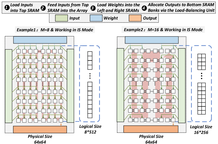
Figure 7. Serpentine Logical Array Remapping under IS Dataflow. Serpentine Logical Array Remapping under IS Dataflow.
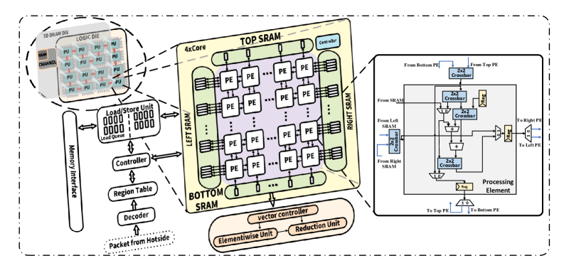
Unlike conventional SA, our design surrounds the PE fabric with four boundary buffers on the top, bottom, left, and right sides. This organization provides the structural basis for flexible remapping under different logical array shapes and dataflows. However, not all four sides require the same degree of flexibility: since fine-grained remapping is only needed along the small- $M$ dimension, multi-port support is required only for weight injection. Specifically, if the array is partitioned into $g$ logical slices, then $g$ weight-injection ports are needed in total. As shown in Figure 6, the central yellow region in the figure corresponds to a single PE array at the core level. We adopt a symmetric left-right boundary organization for the weight side, so that these ports can be distributed across the two boundaries rather than concentrated on one side. For example, when the remapping granularity is 8, only four ports need to be activated on the left boundary and four on the right boundary. This significantly reduces the per-side multi-port requirement of the weight buffer and boundary interconnect under the tight logic-die area budget of 3D-stacked NMP. Accordingly, the left and right boundary buffers can be provisioned with larger capacity, since they consistently act as the weight-side storage and injection buffers under both OS and IS.
Inside each PE, configurable crossbars and register paths support directional data propagation, enabling the logical communication pattern to be reorganized under different sub-array shapes and dataflows. In addition, as shown in Figure 6, the rightmost zoom-in shows the microarchitecture of an individual PE. The bottom-boundary PEs introduce extra interconnect paths to support different output-propagation patterns. The reconfiguration overhead is negligible, as switching the PE mode takes only one cycle.
#### 4.2.2. SNAKE-Like Mapping
On top of this low-cost multi-port organization, we propose a mapping method, termed SNAKE-like mapping, in which the dataflow propagates through the physical PE fabric along a serpentine path, much like the Snake game gradually sweeping across and filling the entire array. Because OS and IS share the same nearest-neighbor systolic fabric and differ primarily in boundary-level operand injection and output propagation, the same physical array organization can support both dataflows. Figure 7 illustrates this remapping under the IS dataflow. A physical $64× 64$ array serves as the fixed PE fabric. In this example, inputs are loaded into the top buffer, weights stream into the array from the left and right buffer, and the output space is distributed across different bottom SRAM banks by the SRAM load-balancing unit. Under this organization, the same physical $64× 64$ array can be remapped into different elongated logical sub-array shapes to better match operators with different small- $M$ dimensions. When $M=8$ , the entire physical array is reorganized into a logical $8× 512$ sub-array. In other words, the original two-dimensional set of 4096 PEs is traversed in a SNAKE-like manner and concatenated into a longer logical computation path, allowing each logical output stream to propagate through the full PE fabric and accumulate continuously. Likewise, when $M=16$ , the same physical array is reorganized into a logical $16× 256$ structure, enabling more parallel logical output streams while preserving a long effective computation path. Although our minimum reconfiguration granularity is 8 rather than 1, this limitation mainly affects a small subset of GEMV-like decode operators with extremely small $M$ (e.g., $M=1$ ), which cannot be perfectly matched by our logical sub-array shapes. This design choice is acceptable because such cases tend to become memory-bound, where execution is dominated by data-supply stalls rather than peak compute occupancy. In such cases, the residual utilization loss has limited impact on end-to-end performance.
#### 4.2.3. Vector Core Design
The vector core is organized around the output buffer of SA, rather than using a separate private SRAM. In this way, the same storage structure serves both as the writeback space for SA results and as the input/intermediate buffer for subsequent vector operations such as softmax, normalization, and other element-wise processing. To support this interaction, output buffer is implemented as a banked 2-read/2-write structure. The SA can write results back to the buffer, while the vector core reads them out for post-processing. A lightweight arbitration logic coordinates array writeback, array readback, and vector-side accesses according to access type and bank conflicts. This organization preserves limited overlap between tensor and vector execution when accesses do not conflict, while keeping the vector-side storage overhead small under the tight logic-die area budget.
#### 4.2.4. Control Logic Design
The vector core originally employs fine-grained control, and we extend this control logic to also manage the systolic mode. As shown in the middle of Figure 6, after the Decoder parses the operator descriptor, the controller centrally dispatches the corresponding commands to the LSU and to the RTAB.
Decoder. The Decoder receives task packets from the host side and parses them into internal execution descriptors for both the systolic core and the vector core. For systolic execution, each matrix-multiply instruction is further split into pipelined sub-stages—Weight Load, Feed First/Second, Drain—to overlap execution and mask PE idle cycles. Control signals flow with operands, minimizing both hardware overhead and reconfiguration latency, similar in spirit to RASA’s pipelining optimizations (Jeong et al., 2021).
Load/Store Unit (LSU). The LSU manages on-chip SRAM at bank granularity, handling mode selection, address allocation, while hiding storage latency. Under different dataflows, it assigns matrix tiles to different boundary SRAMs and schedules their load/feed order accordingly, so that the same physical core can realize different logical operand movements without changing the PE fabric. For vector execution, it also supports the movement of intermediate tiles between the output buffer and vector-side operations.
Region Table (RTAB). The RTAB records the spatial boundaries of each working region together with its corresponding SRAM allocation results under different dataflow. During execution, it continuously tracks the readiness, running, and completion states of all regions, enabling dynamic management of multiple logical sub-arrays.
## 5. MULTI-PU SCHEDULING VIA SPATIAL AND SPATIO-TEMPORAL PARTITIONING
a) Intra-Operator Multi-PU Scheduling.
In this part, we perform multi-core scheduling at the PU granularity. Each PU contains four local reconfigurable SA cores that cooperatively execute the assigned linear operators under a unified systolic dataflow for each operator. As discussed in Section 3.1, the preferred single-core systolic dataflow depends on the relative size of $N$ and $K$ . We therefore turn to the view of MNK-level partitioning.
First, we do not partition the $M$ dimension across PU as described above, and keep the $M$ dimension inside each PU to determine logical array shape and only design multi-PU scheduling over the two dominant dimensions, $N$ and $K$ . Under IS and OS, these two dimensions naturally serve as the spatial and temporal dimensions in different ways. As a result, the multi-PU design space reduces to four partitioning modes.
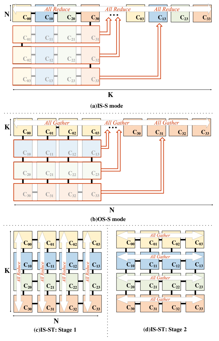
1) IS-S: IS with pure spatial partitioning. In this mode, IS is used as the inter-PU dataflow, and only spatial partitioning is applied across PU. Different PU mainly split the $K$ dimension in space, while each PU locally processes its tiles along the $N$ time dimension.
2) IS-ST: IS with spatio-temporal partitioning. This mode extends IS-S by further partitioning the time dimension. Besides splitting the $K$ dimension in space, it also divides the time dimension $N$ into multiple stages or time blocks.
3) OS-S and 4) OS-ST. Similarly, OS-S partitions the $N$ dimension in space and advances along the $K$ dimension in time. OS-ST further partitions the $K$ dimension into multiple time blocks based on OS-S.
This lightweight interconnect design follows from the regular $N$ - and $K$ -dimension partitioning, which limits inter-PU communication to a few collectives and keeps the structure simple and area-efficient. As shown in Figure 8, the same 16 PU can be organized in two simple logical ways using interconnect: a SNAKE-like $1× 16$ chain, similar to the traversal described above, or a regular $4× 4$ mesh, similar to a conventional array interconnect. The $1× 16$ view is used when one dimension is divided by 16 across the 16 cores, corresponding to IS-S and OS-S. The $4× 4$ view is used when both dimensions are divided by 4 across PU, corresponding to IS-ST and OS-ST.
<details>
<summary>2604.04253v2/x8.png Details</summary>
### Visual Description
## Block Diagram: Parallel Processing Architecture
### Overview
The diagram illustrates a multi-stage parallel processing architecture with four configurations:
1. **IS-S mode** (top-left)
2. **OS-S mode** (top-right)
3. **IS-ST Stage 1** (bottom-left)
4. **IS-ST Stage 2** (bottom-right)
Each configuration uses labeled blocks (C00, C01, ..., C33) and directional arrows to represent data flow operations ("All Reduce" and "All Gather").
---
### Components/Axes
- **Axes**:
- Horizontal axis labeled **N** (left to right).
- Vertical axis labeled **K** (top to bottom).
- **Blocks**:
- Organized in a grid with labels like **C00**, **C10**, **C20**, **C30** (first column), **C01**, **C11**, etc.
- Colors differentiate blocks (e.g., yellow, blue, green, orange), though no explicit legend is provided.
- **Arrows**:
- **Red arrows** labeled "All Reduce" (vertical/horizontal).
- **White arrows** labeled "All Gather" (horizontal/vertical).
---
### Detailed Analysis
#### (a) IS-S Mode
- **Structure**:
- 4 rows (K=4) and 4 columns (N=4).
- Blocks are grouped into 4x4 subgrids (e.g., C00-C03, C10-C13).
- **Flow**:
- Vertical red arrows ("All Reduce") aggregate data upward within each column.
- Horizontal red arrows ("All Reduce") aggregate results across columns.
#### (b) OS-S Mode
- **Structure**:
- Similar 4x4 grid but with reversed flow direction.
- **Flow**:
- Horizontal white arrows ("All Gather") collect data across rows.
- Vertical white arrows ("All Gather") propagate results downward.
#### (c) IS-ST Stage 1
- **Flow**:
- Vertical red arrows ("All Reduce") operate within each column (K-axis).
- No horizontal aggregation yet.
#### (d) IS-ST Stage 2
- **Flow**:
- Horizontal white arrows ("All Gather") aggregate results across rows (N-axis).
---
### Key Observations
1. **Operation Order**:
- IS-S mode prioritizes vertical reduction first, then horizontal.
- OS-S mode reverses this, starting with horizontal gathering.
2. **Stage Progression**:
- IS-ST stages show a two-phase process: reduction (Stage 1) followed by gathering (Stage 2).
3. **Block Grouping**:
- Blocks are organized in subgrids (e.g., C00-C03, C10-C13), suggesting hierarchical processing.
---
### Interpretation
This diagram models a distributed computing workflow, likely for tasks like matrix operations or data aggregation.
- **IS-S vs. OS-S**:
- IS-S reduces data vertically first, minimizing intermediate data movement.
- OS-S gathers data horizontally first, which may optimize for row-wise dependencies.
- **IS-ST Stages**:
- Stage 1 focuses on intra-column reduction, while Stage 2 handles inter-row gathering.
- **Efficiency Implications**:
- The choice of operation order (reduce vs. gather) impacts communication overhead in parallel systems.
- IS-ST’s staged approach balances computational and communication costs.
No explicit numerical values or trends are provided, but the directional flow and operation labels define the algorithmic logic.
</details>
Figure 8. Logical Inter-PU Organizations for Representative Partitioning Modes Logical Inter-PU Organizations for the Four Partitioning Modes
b) Operator-Specific Scheduling Analysis. These four modes define the MNK-level scheduling space for the major linear kernels in decode. Among these scheduling candidates, the final mode is selected based on the overall operator-specific considerations described below. We first decide which operators are scheduled within this space and which are better handled separately. We also analyze tile-level overlap between these linear operators and the following nonlinear stages to reduce end-to-end latency.
For the $QK$ and $AV$ head-level operators in attention, the computation of one head is usually small, and thus cannot fully hide the memory access latency from 3D-stacked memory. Therefore, we follow a strategy similar to Stratum (Pan et al., 2025): we mainly use head-level parallelism (partition the $M$ dimension), map different heads to different PU, and improve utilization by interleaving the linear stage and the Softmax/reduction stage of different heads within the same group.
For the remaining decode operators that account for most of the execution time, such as projection operators and expert FFNs in MoE layers, we treat them as independent GEMM/GEMV kernels and analyze their dataflow choices under the above multi-PU spatial/spatio-temporal framework.
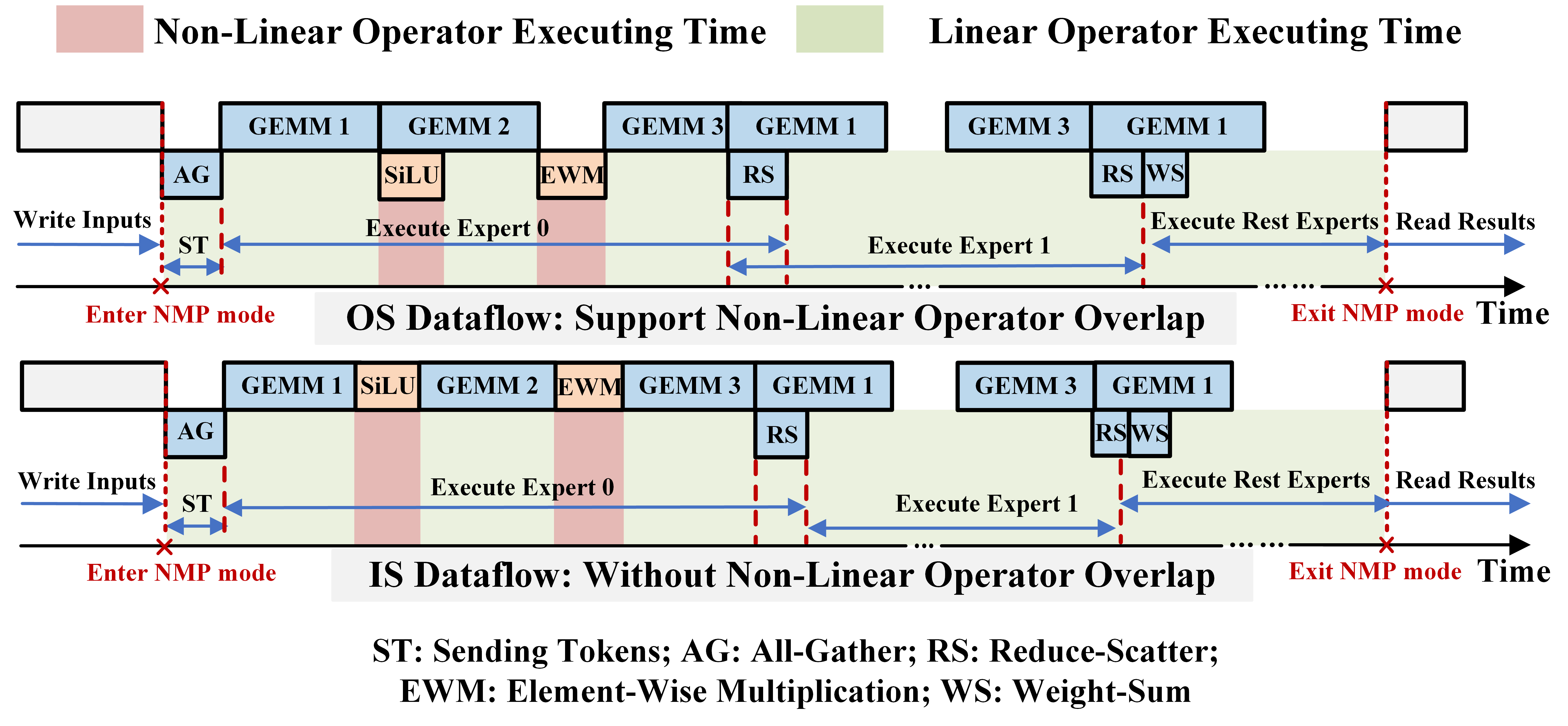
In general, OS dataflow is more favorable for direct tile-level overlap between linear and nonlinear stages, because an output tile can be consumed by the following nonlinear operator as soon as its in-array reduction is completed. By contrast, under IS dataflow, such direct overlap is usually weaker, since an output tile often becomes available only after accumulation along the temporal dimension is finished. Below we instantiate this framework with a representative decode scheduling policy in Fig. 9 for MoE layer in DeepSeek 236B (batch = 8). Still, IS can remain favorable when it shortens the critical GEMM latency, and it may also exploit overlap across independent operator branches. In practice, the realizable overlap further depends on whether the following stage is tile-foldable, as well as on the communication pattern (e.g., all-gather vs. all-reduce) and buffer-capacity constraints.
Overall, this yields a compact and deployment-friendly scheduling space, where each operator only needs to evaluate four candidate strategies. For a given LLM, our simulator performs this lightweight search and selects the best partitioning strategy for each operator and assembles the corresponding best scheduling combination for the full network.
<details>
<summary>2604.04253v2/figure/moe.png Details</summary>
### Visual Description
## Diagram: Non-Linear Operator Executing Time Comparison
### Overview
The image compares two computational dataflows for executing machine learning operations:
1. **OS Dataflow**: Supports non-linear operator overlap (red-shaded regions).
2. **IS Dataflow**: Processes operations sequentially without overlap (no red shading).
Both workflows include stages like input writing, token sending, expert execution, and result reading, with timing marked by red dashed lines.
### Components/Axes
- **X-axis**: Time progression (left to right).
- **Y-axis**: Two dataflows (OS Dataflow at top, IS Dataflow at bottom).
- **Legend**:
- **Red**: Non-linear operator executing time.
- **Green**: Linear operator executing time.
- **Key Labels**:
- **AG**: All-Gather (blue).
- **SiLU**: Sigmoid Linear Unit (orange).
- **GEMM**: General Matrix Multiply (blue).
- **EWM**: Element-Wise Multiplication (orange).
- **RS**: Reduce-Scatter (blue).
- **WS**: Weight-Sum (blue).
- **ST**: Sending Tokens (blue arrows).
### Detailed Analysis
#### OS Dataflow (Top Section)
1. **Non-Linear Overlap**:
- Red-shaded regions (SiLU, EWM) overlap with green-shaded GEMM operations.
- Example: SiLU (non-linear) overlaps with GEMM 2 (linear) during "Execute Expert 0."
2. **Flow Sequence**:
- Inputs → AG → SiLU → GEMM 1 → GEMM 2 → EWM → GEMM 3 → RS → Execute Experts → Read Results.
3. **NMP Mode**:
- "Enter NMP mode" (red X) marks the start, and "Exit NMP mode" marks the end of non-linear operations.
#### IS Dataflow (Bottom Section)
1. **No Overlap**:
- Red-shaded regions (SiLU, EWM) are isolated from green-shaded GEMM operations.
- Example: SiLU (non-linear) executes fully before GEMM 1 (linear) begins.
2. **Flow Sequence**:
- Inputs → AG → SiLU → GEMM 1 → GEMM 2 → EWM → GEMM 3 → RS → Execute Experts → Read Results.
3. **NMP Mode**:
- Same entry/exit markers as OS Dataflow but no overlapping execution.
### Key Observations
- **Overlap Impact**: OS Dataflow reduces total execution time by overlapping non-linear (red) and linear (green) operations.
- **Sequential Bottlenecks**: IS Dataflow avoids overlap but may increase latency due to strict sequential processing.
- **Component Roles**:
- GEMM operations dominate linear execution (green).
- SiLU and EWM introduce non-linear complexity (red).
- **Token Flow**: Blue arrows (ST) indicate token transmission between stages.
### Interpretation
The diagram illustrates a trade-off between computational efficiency and simplicity:
- **OS Dataflow** optimizes time by overlapping non-linear and linear operations, critical for real-time systems.
- **IS Dataflow** prioritizes simplicity by isolating operations, potentially useful for debugging or latency-insensitive tasks.
- **Non-Linear Overlap**: The red-shaded regions in OS Dataflow highlight how modern frameworks exploit parallelism to accelerate training/inference.
- **NMP Mode**: Likely a "Non-Linear Mode" enabling concurrent execution of mixed operation types.
The image emphasizes the importance of operator overlap in reducing end-to-end latency, a key consideration in distributed machine learning systems.
</details>
Figure 9. A Representative MoE-Expert Example of Linear–Nonlinear Overlap under OS and IS Dataflows. A diagram showing Overlap.
## 6. EVALUATION
### 6.1. Experimental Setup
#### 6.1.1. Benchmark
We follow Helios (Li et al., 2026) in benchmark selection and use OPT (Zhang et al., 2022), LLaMA3 (Dubey et al., 2024), Mixtral (Jiang et al., 2024), Qwen3 (Yang et al., 2025), and DeepSeek (DeepSeek-AI et al., 2024). These models cover both dense and MoE LLMs. We use model-specific input/output length settings for decode and serving evaluation. Detailed configurations are summarized in Table 1. We follow prior work (Yun et al., 2024) and model MoE expert activation using a uniform routing distribution during evaluation.
<details>
<summary>2604.04253v2/x9.png Details</summary>
### Visual Description
## Line Graphs: Latency Comparison Across Hardware Configurations
### Overview
The image contains multiple line graphs comparing the performance of different systems (MAC tree, GPU, 4x48 SA, 8x288 SA, and "Ours") across various hardware configurations. Each graph tracks two metrics: **Normal E2E Latency** (top row) and **Normal TBT Latency** (bottom row). The x-axis represents different hardware setups (e.g., CPU, GPU, MAC tree, etc.), while the y-axis measures latency in arbitrary units.
### Components/Axes
- **X-axis (Categories)**:
- CPU, GPU, MAC tree, P90, P50, P99, P10, P1, P0.1, P0.01, P0.001, P0.0001, P0.00001, P0.000001.
- **Y-axis (Metrics)**:
- **Top Row**: Normal E2E Latency (units: 0–6).
- **Bottom Row**: Normal TBT Latency (units: 0–6).
- **Legend**:
- **Colors**:
- MAC tree: Blue (circle).
- GPU: Light blue (triangle).
- 4x48 SA: Orange (triangle).
- 8x288 SA: Purple (triangle).
- "Ours": Dark purple (triangle).
### Detailed Analysis
#### Top Row (Normal E2E Latency)
1. **CPU**:
- "Ours" (dark purple) shows a steady increase from ~2.0 to ~4.0.
- 8x288 SA (purple) starts at ~2.0, peaks at ~4.5, then drops to ~3.0.
- MAC tree (blue) remains flat at ~2.0.
2. **GPU**:
- "Ours" rises sharply from ~1.0 to ~4.0.
- 8x288 SA (purple) increases gradually from ~1.0 to ~3.5.
- MAC tree (blue) stays flat at ~1.0.
3. **MAC tree**:
- "Ours" increases from ~1.0 to ~2.5.
- 8x288 SA (purple) rises from ~1.0 to ~3.0.
- MAC tree (blue) remains flat at ~1.0.
4. **P90/P50/P99**:
- "Ours" shows moderate increases (e.g., P90: ~2.0 → ~3.0).
- 8x288 SA (purple) has steeper rises (e.g., P90: ~2.0 → ~4.0).
- MAC tree (blue) remains flat.
5. **P10/P1/P0.1**:
- "Ours" increases slightly (e.g., P1: ~1.5 → ~2.0).
- 8x288 SA (purple) spikes (e.g., P1: ~1.0 → ~3.0).
- MAC tree (blue) stays flat.
#### Bottom Row (Normal TBT Latency)
1. **CPU**:
- "Ours" (dark purple) increases from ~1.0 to ~2.5.
- 8x288 SA (purple) rises from ~1.0 to ~3.0.
- MAC tree (blue) remains flat at ~1.0.
2. **GPU**:
- "Ours" increases from ~1.0 to ~3.5.
- 8x288 SA (purple) rises from ~1.0 to ~4.0.
- MAC tree (blue) stays flat at ~1.0.
3. **MAC tree**:
- "Ours" increases from ~1.0 to ~2.0.
- 8x288 SA (purple) rises from ~1.0 to ~3.0.
- MAC tree (blue) remains flat.
4. **P90/P50/P99**:
- "Ours" shows moderate increases (e.g., P90: ~1.5 → ~2.5).
- 8x288 SA (purple) has steeper rises (e.g., P90: ~1.0 → ~4.0).
- MAC tree (blue) stays flat.
5. **P10/P1/P0.1**:
- "Ours" increases slightly (e.g., P1: ~1.0 → ~1.5).
- 8x288 SA (purple) spikes (e.g., P1: ~1.0 → ~3.0).
- MAC tree (blue) stays flat.
### Key Observations
- **"Ours" (dark purple)**: Consistently shows lower latency than other systems in most configurations, with gradual increases.
- **8x288 SA (purple)**: Exhibits significant latency spikes, especially in GPU and MAC tree configurations.
- **MAC tree (blue)**: Maintains flat latency across all configurations, suggesting stable performance.
- **GPU (light blue)**: Shows moderate latency increases, with "Ours" outperforming others.
- **P90/P50/P99**: Higher percentiles (e.g., P99) show more pronounced latency differences between systems.
### Interpretation
The data suggests that the "Ours" system is the most efficient, with lower latency across most hardware configurations. The 8x288 SA system, while performing well in some cases, exhibits higher latency spikes, potentially due to scalability or resource contention issues. The MAC tree configuration demonstrates the most stable performance, with minimal latency variation. These trends highlight the importance of system design and hardware optimization in latency-sensitive applications.
</details>
Figure 10. Normalized Serving Latency Under Different Request Rates servinglatency
#### 6.1.2. Baseline
System template. Since we focus on compute-substrate comparison rather than full-system redesign, we adopt Stratum (Pan et al., 2025) as a common HBM3-class 3D-stacked NMP template. It represents one of the most aggressive and well-documented prior designs in terms of internal DRAM bandwidth and active logic-die compute budget. Accordingly, we reuse its memory-system assumptions, including DRAM organization, timing, and energy parameters, and fix the effective DRAM bandwidth at 24 TB/s, the midpoint of Stratum’s reported range.
Baseline compute substrates. Under this common system template, we instantiate a MAC-Tree design as the representative baseline compute substrate. To further isolate the benefit of reconfigurability, we also implement two fixed-shape SA baselines: a square $48× 48$ array and a long $8× 288$ array. Under the same 3D-NMP logic-die constraints, these designs represent practical fixed-shape alternatives without the microarchitectural flexibility and area optimization enabled by our design. We also use GPU as the baseline.
Area-normalized comparison. Since our architecture adopts a compute hierarchy structurally similar to Stratum, we use the same number of PUs under the same logic-die area budget for all designs, enabling a direct area-normalized comparison. All other system-level assumptions are kept unchanged.
Frequency assumption. The fixed-shape baselines are assumed to operate at up to 1 GHz, whereas our reconfigurable design targets 800 MHz due to the additional routing constraints introduced by reconfigurability. Therefore, our comparison is area-normalized and implementation-aware, rather than iso-frequency.
#### 6.1.3. Modeling
Using SystemVerilog, we implement our architecture by modifying PLENA (Wu et al., 2025), a representative LLM SA design, and adapt its original flattened systolic substrate into a reconfigurable SA for the 3D-stacked near-memory setting configured in IEEE 754 FP16 under the 7 nm ASAP7 predictive PDK (Clark et al., 2016). The local buffer on the logic die is implemented as SRAM macros, modeled using FinCACTI (Shafaei et al., 2014) and calibrated with publicly available SRAM specifications (Chang et al., 2017). Dynamic energy is estimated from the post-synthesis gate-level netlist with switching activity annotated from simulation.
For kernel-level performance modeling, we build on Scale-Sim v3 (Raj et al., 2025), which integrates the Ramulator (Kim et al., 2015) memory model, and extend it to capture SA execution in a 3D-NMP setting, including multi-PU interconnection and vector core.
<details>
<summary>2604.04253v2/x10.png Details</summary>
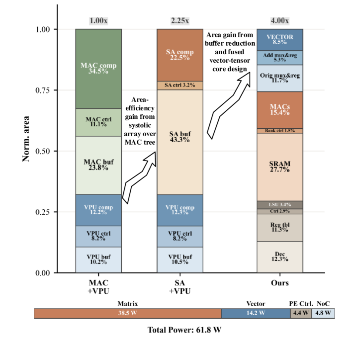
### Visual Description
## Bar Chart: Normalized Area Comparison Across Technologies
### Overview
The chart compares normalized area usage across three technology categories: **Matrix**, **SA**, and **Ours**. Each category is segmented into components (e.g., MAC comp, SA buf, SRAM) with color-coded proportions. Arrows indicate efficiency gains, and power consumption values (in watts) are labeled at the base of each bar. Total power consumption is 61.8 W.
---
### Components/Axes
- **Y-axis**: "Norm. area" (normalized area), scaled from 0.00 to 1.00 in increments of 0.25.
- **X-axis**: Three categories: **Matrix**, **SA**, **Ours**.
- **Legend**: Located at the bottom, mapping colors to components:
- Green: MAC comp, MAC ctrl
- Blue: VPU comp, VPU ctrl
- Orange: SA comp, SA buf
- Beige: SA buf, MAC buf
- Light orange: SRAM
- Gray: Rest, Ctrl, NoC
- Dark blue: Vector, Add, PE Ctrl, NoC
---
### Detailed Analysis
#### Matrix
- **MAC comp**: 24.5% (green)
- **MAC ctrl**: 11.3% (light green)
- **MAC buf**: 23.8% (beige)
- **VPU comp**: 12.3% (blue)
- **VPU ctrl**: 8.3% (dark blue)
- **VPU buf**: 10.2% (light blue)
- **Total power**: 38.5 W
#### SA
- **SA comp**: 22.5% (orange)
- **SA buf**: 43.5% (beige)
- **SA ctrl**: 13.3% (dark blue)
- **Total power**: 14.3 W
#### Ours
- **SRAM**: 27.7% (light orange)
- **Rest**: 11.5% (gray)
- **Ctrl**: 3.4% (gray)
- **NoC**: 4.8% (dark blue)
- **PE Ctrl**: 12.5% (light blue)
- **Total power**: 4.8 W
---
### Key Observations
1. **Power Consumption**:
- Matrix consumes the most power (38.5 W), followed by SA (14.3 W), and Ours (4.8 W).
- Total power across all categories sums to 61.8 W.
2. **Area Efficiency**:
- Arrows indicate **area efficiency gains** from SA to Ours, despite Ours having higher normalized area (4.00%) compared to SA (2.25%).
3. **Component Dominance**:
- **SRAM** dominates the "Ours" category (27.7%).
- **SA buf** is the largest component in SA (43.5%).
4. **Efficiency Gains**:
- Arrows highlight reductions in buffer usage and fused core design improvements.
---
### Interpretation
The chart demonstrates a trade-off between **power consumption** and **normalized area** across technologies:
- **Matrix** prioritizes performance but has high power and area usage.
- **SA** improves efficiency (lower power, smaller area) but still relies heavily on buffers (SA buf: 43.5%).
- **Ours** achieves the lowest power (4.8 W) but uses more normalized area (4.00%), likely due to SRAM dominance. The efficiency gains from buffer reduction and fused core design (noted in arrows) suggest architectural optimizations that reduce power at the cost of area.
The data implies that **Ours** balances power efficiency and area usage better than SA, while Matrix remains the least efficient. The inclusion of SRAM in "Ours" may reflect a design choice for faster access at the expense of area.
</details>
Figure 11. Normalized PU-level Area and Power Breakdown Normalized area breakdown and compute-area efficiency
For end-to-end serving evaluation, as well as GPU and MAC-Tree baseline characterization, we build on Duplex’s system-level serving framework (Yun et al., 2024), including Poisson-based request injection under varying arrival rates, continuous batching, and latency accounting. We use NVIDIA H100 as the common prefill engine across all compared systems, and also use H100-only decoding as one baseline. Within the Duplex-based simulator, we retain its internal GPU and NVLink models and incorporate a Stratum-configured MAC-Tree backend for comparison. We evaluate all models on an 8-device system with tensor parallelism degree TP=8. Although our reconfigurable SA can potentially support more flexible scheduling for MoE expert layer in 3D NMP (Huang et al., 2025), we intentionally retain TP for these layers in this work as in (Pan et al., 2025; Yun et al., 2024).
Table 1. Architectural configurations of evaluated models.
| OPT 66B | 64 | (9216, 36864) | (72, 72) | Dense, MHA |
| --- | --- | --- | --- | --- |
| LLaMA3 70B | 80 | (8192, 28672) | (64, 8) | Dense, GQA |
| Mixtral 8 $×$ 22B | 56 | (6144, 16384) | (48, 8) | MoE, E=8, top-2 |
| Qwen3 30B-A3B | 48 | (2048, 768) | (32, 4) | MoE, E=128, top-8 |
| DeepSeek 236B | 60 | (5120, 1536) | (128, 128) | MoE, E=160, top-8, MLA |
### 6.2. Area Breakdown and Thermal Characterization
Figure 11 compares the normalized area breakdown and compute-area efficiency of three RTL-implemented designs at single-PU granularity under the same PU-level area budget of 2.35 mm 2. For fairness, each design uses the largest feasible compute-unit configuration under this budget: the MAC-Tree baseline adopts a $16× 16× 16$ organization, the conventional SA baselines use $4× 48× 48$ , and our design uses $4× 64× 64$ .
Replacing the MAC-Tree engine with SA already brings a clear improvement: SA + Vector Core reaches 2.25 $×$ higher compute-area efficiency. This gain mainly comes from the structure of the SA with higher compute density. Our design further improves area efficiency in two ways mentioned before, and achieves 4.00 $×$ compute-area efficiency over the MAC Tree.
<details>
<summary>2604.04253v2/x11.png Details</summary>
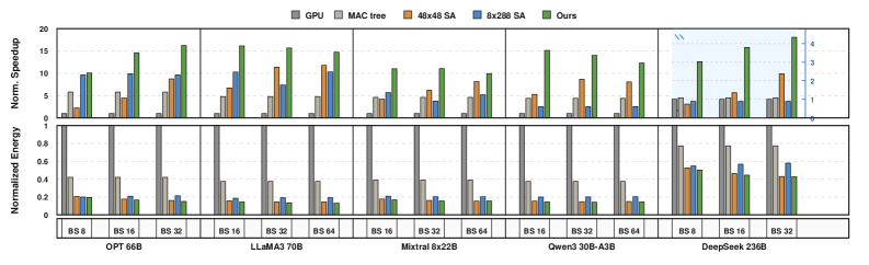
### Visual Description
## Bar Chart: Algorithm Performance Comparison
### Overview
The image is a grouped bar chart comparing the performance of multiple algorithms across two metrics: **Normalized Energy** and **Normalized Speedup**. The chart evaluates seven algorithms (OPT 66B, LLaMA3 70B, Mixtra 8x22B, Owen3 30B-A3B, DeepSeek 236B) against five baseline methods (GPU, MAC tree, 48x48 SA, 8x288 SA, and "Ours"). Each algorithm is represented by a cluster of five bars, with colors corresponding to the legend.
### Components/Axes
- **X-axis**: Algorithms (OPT 66B, LLaMA3 70B, Mixtra 8x22B, Owen3 30B-A3B, DeepSeek 236B).
- **Y-axis (Top)**: Normalized Speedup (scale: 0–20).
- **Y-axis (Bottom)**: Normalized Energy (scale: 0–1).
- **Legend**:
- Gray: GPU
- Light Gray: MAC tree
- Orange: 48x48 SA
- Blue: 8x288 SA
- Green: Ours
### Detailed Analysis
#### Normalized Speedup (Top Y-axis)
- **OPT 66B**:
- GPU: ~10
- MAC tree: ~6
- 48x48 SA: ~5
- 8x288 SA: ~10
- Ours: ~15
- **LLaMA3 70B**:
- GPU: ~10
- MAC tree: ~5
- 48x48 SA: ~12
- 8x288 SA: ~8
- Ours: ~16
- **Mixtra 8x22B**:
- GPU: ~5
- MAC tree: ~4
- 48x48 SA: ~7
- 8x288 SA: ~6
- Ours: ~11
- **Owen3 30B-A3B**:
- GPU: ~5
- MAC tree: ~4
- 48x48 SA: ~9
- 8x288 SA: ~3
- Ours: ~14
- **DeepSeek 236B**:
- GPU: ~4
- MAC tree: ~3
- 48x48 SA: ~6
- 8x288 SA: ~4
- Ours: ~17
#### Normalized Energy (Bottom Y-axis)
- **OPT 66B**:
- GPU: ~0.4
- MAC tree: ~0.2
- 48x48 SA: ~0.2
- 8x288 SA: ~0.2
- Ours: ~0.15
- **LLaMA3 70B**:
- GPU: ~0.35
- MAC tree: ~0.25
- 48x48 SA: ~0.15
- 8x288 SA: ~0.1
- Ours: ~0.1
- **Mixtra 8x22B**:
- GPU: ~0.3
- MAC tree: ~0.2
- 48x48 SA: ~0.15
- 8x288 SA: ~0.1
- Ours: ~0.1
- **Owen3 30B-A3B**:
- GPU: ~0.3
- MAC tree: ~0.25
- 48x48 SA: ~0.15
- 8x288 SA: ~0.1
- Ours: ~0.1
- **DeepSeek 236B**:
- GPU: ~0.5
- MAC tree: ~0.4
- 48x48 SA: ~0.3
- 8x288 SA: ~0.3
- Ours: ~0.25
### Key Observations
1. **"Ours" consistently outperforms all baselines in normalized speedup** across all algorithms, with values ranging from 11 to 17 (vs. GPU’s 4–10).
2. **GPU has the highest speedup** but also the highest energy consumption (0.4–0.5), while "Ours" achieves lower energy (0.1–0.25).
3. **MAC tree underperforms in speedup** (3–6) but has moderate energy use (0.2–0.4).
4. **48x48 SA and 8x288 SA show mixed results**:
- 48x48 SA has higher speedup (5–12) but similar energy to "Ours".
- 8x288 SA has lower speedup (3–8) and higher energy than "Ours".
### Interpretation
The data suggests that **"Ours" algorithm achieves superior speedup with competitive energy efficiency** compared to all baselines. GPU, while fast, consumes significantly more energy, making it less optimal for energy-constrained scenarios. MAC tree’s low speedup indicates potential inefficiencies in its design. The 48x48 SA and 8x288 SA trade-offs between speed and energy highlight the importance of algorithm-specific optimizations. The chart underscores the need for balancing computational speed and energy consumption in algorithm selection.
</details>
Figure 12. Normalized Decode Performance and Energy Efficiency decodingnormmetrics
From the area breakdown, additional Muxes and Regs at the PE level for SA reconfigurability account for 6.0% of the total area, which is offset by the area saved. Notably, although our buffers now include multi-port SRAMs to support fine-grained reconfigurability, the total buffering-related area still decreases from 53.6% in SA + Vector Core to 28.1% in Our Work, and this released area is primarily reallocated to compute units. The vector-core share also decreases to 8.8%, with part of it further reallocated to fine-grained control logic and compute units.
Following Stratum, we use HotSpot (Zhang et al., 2015) to evaluate the 3D thermal behavior under the same package and cooling assumptions, and define the logic-die power budget as the maximum logic power that keeps the peak temperature below 85°C (Han et al., 2021). For practicality, we reduce the effective DRAM bandwidth from 30.34 TB/s to 24 TB/s, which lowers DRAM power and leaves more thermal budget for the logic die. We also use a lower logic-die frequency, 800 MHz, which further reduces dynamic power. As a result, the allowable logic-die power budget is about 62 W. Figure 11 shows the peak-performance power breakdown of the logic die under the thermal operating point described above. The total logic-die power is 61.8 W, including 38.5 W for Matrix unit, 14.2 W for Vector unit, 4.4 W for PE control, and 4.8 W for NoC.
### 6.3. Decode Performance Evaluation
Prior work (He et al., 2025) has established that thermal dissipation at the logic die is the primary bottleneck in 3D-stacked systems. Therefore, this work focuses specifically on comparing the energy consumption of the logic die. As shown in Fig. 12, compared with GPU, our design achieves an average of $11.47×$ speedup and $5.74×$ higher energy efficiency. Compared with the MAC-Tree baseline, our design achieves an average of $2.90×$ speedup and $2.40×$ higher energy efficiency. These gains come from both a denser compute organization under the tight logic-die area budget and better workload matching through reconfigurable dataflow and Multi-PU scheduling. Meanwhile, in addition to lower clock frequency and DRAM bandwidth, by reducing unnecessary on-chip SRAM accesses and shortening execution time, our design also improves energy efficiency.
Further comparison with the two fixed-shape SA baselines shows that reconfigurability itself is a key source of the gain. Compared with the $48× 48$ SA baseline, our design achieves an average of $2.33×$ speedup and $1.05×$ higher energy efficiency; compared with the $8× 288$ SA baseline, it achieves $3.00×$ speedup and $1.31×$ higher energy efficiency on average. Although a fixed-shape SA may achieve better local reuse for some operators, the reconfigurable SA can select a more suitable array shape for each operator, thereby improving both throughput and memory-access energy efficiency.
### 6.4. Serving Performance Evaluation
Fig. 10 presents the latency results of five models under two serving scenarios: the top row reports end-to-end (E2E) latency under full serving, while the bottom row reports time-between-token (TBT) latency under decoding stress tests.
Fig. 10 shows normalized serving latency under different request rates for 8K-input and 1K-output requests. The x-axis is the normalized request rate, and the y-axis reports normalized latency, including both end-to-end (E2E) latency and time-between-tokens (TBT) latency, with our design as the baseline.
Specifically, the GPU baseline exhibits substantially higher latency. As shown in the figure, GPU E2E latency is typically around $1.5×$ – $3.0×$ that of our design, while its TBT latency usually reaches about $1.5×$ – $4.0×$ . MAC-Tree is generally the closest baseline to our design, with E2E latency mostly around $1.1×$ – $2.3×$ that of our design and TBT latency mostly around $1.3×$ – $2.2×$ . As the request rate increases and the effective decode batch becomes larger, the area-efficiency advantage of SA becomes more consistent. Since our design can further adapt both array shape and mapping strategy to the workload, it gradually widens the gap over MAC-Tree.
For fixed-shape SA, the $48× 48$ SA consistently performs better than the $8× 288$ SA, but both remain inferior to our design. In particular, the $48× 48$ SA still shows about $1.1×$ – $2.4×$ E2E latency and $1.1×$ – $2.2×$ TBT latency of our design, while the $8× 288$ SA is often worse, with TBT latency reaching about $1.5×$ – $4.5×$ . This suggests that a near-square array is more robust than a highly elongated one under serving workloads. Still, both fixed-shape designs suffer from workload-shape sensitivity, whereas our reconfigurable array can sustain higher utilization across more diverse decode workloads.
### 6.5. Multi-PU Scheduling Analysis
<details>
<summary>2604.04253v2/x12.png Details</summary>
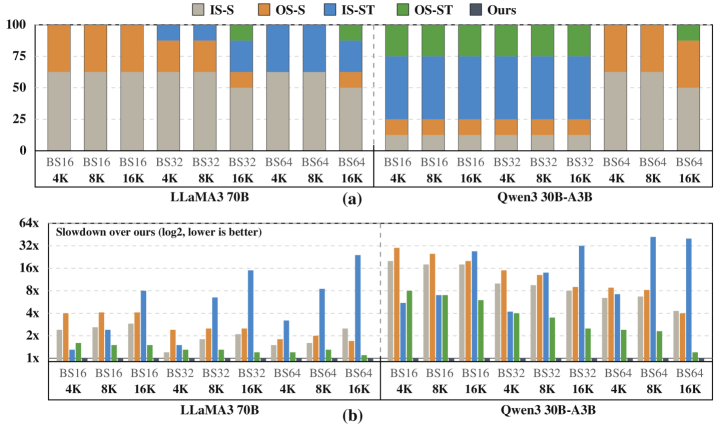
### Visual Description
## Bar Chart: Model Performance Comparison Across Methods and Sizes
### Overview
The image presents a comparative bar chart analyzing the performance of different methods (IS-S, OS-S, IS-ST, OS-ST, and "Ours") across two large language models (LLaMA3 70B and Qwen3 30B-A3B) at varying input sizes (4K, 8K, 16K). A secondary y-axis visualizes slowdown factors relative to the "Ours" method.
### Components/Axes
- **X-axis**: Model sizes (4K, 8K, 16K) and methods (IS-S, OS-S, IS-ST, OS-ST, "Ours").
- **Y-axis (Left)**: Percentage contribution (0–100%) of each method.
- **Y-axis (Right)**: Slowdown factor (log2 scale, lower is better).
- **Legend**: Located on the right, with colors:
- Gray: IS-S
- Orange: OS-S
- Blue: IS-ST
- Green: OS-ST
- Black: "Ours"
- **Secondary Y-axis**: Positioned on the far right, labeled "Slowdown over ours (log2, lower is better)".
### Detailed Analysis
#### LLaMA3 70B (Left Section)
- **4K**:
- "Ours" (black) dominates with ~60%.
- IS-S (gray) contributes ~30%, OS-S (orange) ~10%.
- **8K**:
- "Ours" increases to ~65%.
- IS-S drops to ~25%, OS-S ~10%.
- **16K**:
- "Ours" peaks at ~70%.
- IS-S ~20%, OS-S ~10%.
#### Qwen3 30B-A3B (Right Section)
- **4K**:
- "Ours" ~50%, IS-S ~30%, OS-S ~10%.
- **8K**:
- "Ours" ~55%, IS-S ~35%, OS-S ~10%.
- **16K**:
- "Ours" ~60%, IS-S ~25%, OS-S ~15%.
#### Slowdown Factors (Secondary Y-axis)
- **LLaMA3 70B**:
- IS-ST (blue) shows the highest slowdown (~8x at 16K).
- "Ours" remains at 1x across all sizes.
- **Qwen3 30B-A3B**:
- IS-ST slowdown peaks at ~16x (16K).
- OS-ST (green) shows moderate slowdown (~4x at 16K).
### Key Observations
1. **"Ours" Method Dominance**:
- Consistently achieves the highest percentage contribution across all model sizes and methods.
- Maintains a 1x slowdown factor, indicating optimal efficiency.
2. **Performance Degradation**:
- IS-ST and OS-ST methods exhibit significant slowdowns, especially at larger input sizes (16K).
- IS-S and OS-S methods show diminishing returns as model size increases.
3. **Model-Specific Trends**:
- LLaMA3 70B demonstrates slightly better performance for "Ours" compared to Qwen3 30B-A3B.
- Qwen3 30B-A3B experiences higher slowdowns for IS-ST at larger sizes.
### Interpretation
The data highlights the superiority of the "Ours" method in balancing performance and efficiency. Its consistent dominance across model sizes suggests it is well-suited for scaling, while other methods suffer from inefficiencies (e.g., IS-ST’s 16x slowdown at 16K for Qwen3). The log2 slowdown scale emphasizes exponential inefficiencies in competing methods, particularly for larger models. This underscores the importance of optimizing methods for scalability in large language model applications.
</details>
Figure 13. Scheduling Mode Selection and Fixed-Mode Slowdown (a) Per-operator Partitioning Mode Distribution (b) Performance Comparison: Fixed Scheduling Mode vs. Per-Layer Flexible Scheduling
With logical array shape determined, Figure 13 (a) shows the distribution of per-operator selected multi-PU scheduling modes across all operators under different batch sizes and input sequence lengths. We include one dense model (LLaMA3 70B) and one MoE model (Qwen3 30B-A3B) for comparison. For the dense model, strategy selection is highly concentrated, with IS-S dominating (59.7%), followed by OS-S (25.0%), IS-ST (12.5%), and OS-ST (2.8%). In contrast, the MoE model exhibits a more balanced distribution across IS-ST (33.3%), IS-S (27.8%), OS-S (20.8%), and OS-ST (18.1%). This illustrates that optimal partitioning strategies vary significantly across operators, making it challenging for any single fixed strategy to achieve consistently high utilization.
Figure 13 (b) compares the slowdown of using one fixed scheduling mode for all operators against our per-operator flexible scheduler. For LLaMA3 70B, the best fixed strategy (OS-ST) still incurs a slowdown of 1.04 $×$ –1.56 $×$ relative to the per-operator scheduler. The impact is more pronounced for Qwen3 30B-A3B, where the best fixed policy experiences a slowdown of 1.18 $×$ –6.43 $×$ . These results highlight that a per-operator, workload-adaptive strategy is essential to approach optimal decode performance across diverse operators and sequence lengths.
### 6.6. Array-Shape and Buffer Trade-offs
<details>
<summary>2604.04253v2/x13.png Details</summary>
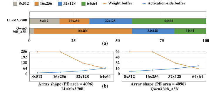
### Visual Description
## Bar Chart: Model Component Distribution (LLaMA3 70B vs Qwen3 30B_A3B)
### Overview
The bar chart compares the distribution of array shapes and buffers for two models: LLaMA3 70B and Qwen3 30B_A3B. The x-axis represents a normalized scale (0–100), while the y-axis lists the models. The legend defines six categories: array shapes (8x512, 16x256, 32x128, 64x64) and buffers (Weight buffer, Activation-side buffer).
### Components/Axes
- **X-axis**: Normalized scale (0–100)
- **Y-axis**: Models (LLaMA3 70B, Qwen3 30B_A3B)
- **Legend**:
- 8x512 (gray)
- 16x256 (orange)
- 32x128 (blue)
- 64x64 (green)
- Weight buffer (orange)
- Activation-side buffer (blue)
### Detailed Analysis
- **LLaMA3 70B**:
- 8x512 (gray): ~25% of the bar
- 16x256 (orange): ~40% of the bar
- 32x128 (blue): ~20% of the bar
- 64x64 (green): ~15% of the bar
- **Qwen3 30B_A3B**:
- 16x256 (orange): ~70% of the bar
- 32x128 (blue): ~20% of the bar
- 64x64 (green): ~10% of the bar
### Key Observations
- LLaMA3 70B uses a more balanced distribution of array shapes, with 8x512 being the largest segment.
- Qwen3 30B_A3B heavily relies on 16x256, with minimal use of 8x512 and 64x64.
- The Weight buffer and Activation-side buffer are not explicitly shown in the bar chart but are referenced in the legend.
### Interpretation
The bar chart highlights differences in how the two models allocate computational resources across array shapes. LLaMA3 70B’s broader distribution suggests flexibility, while Qwen3 30B_A3B’s focus on 16x256 may optimize for specific performance metrics. The absence of explicit buffer data in the bar chart implies these components are either negligible or integrated into the array shape allocations.
---
## Line Graphs: PE Area vs Array Shape (LLaMA3 70B and Qwen3 30B_A3B)
### Overview
Two line graphs compare the PE (Processing Element) area (4096) for different array shapes (8x512, 16x256, 32x128, 64x64) across two models. The x-axis lists array shapes, and the y-axis shows PE area. The legend distinguishes Weight buffer (orange) and Activation-side buffer (blue).
### Components/Axes
- **X-axis**: Array shapes (8x512, 16x256, 32x128, 64x64)
- **Y-axis**: PE area (4096)
- **Legend**:
- Weight buffer (orange)
- Activation-side buffer (blue)
### Detailed Analysis
- **LLaMA3 70B**:
- **Weight buffer (orange)**:
- 8x512: 256
- 16x256: 192
- 32x128: 128
- 64x64: 64
- **Activation-side buffer (blue)**:
- 8x512: 0
- 16x256: 0
- 32x128: 0
- 64x64: 64
- **Qwen3 30B_A3B**:
- **Weight buffer (orange)**:
- 8x512: 256
- 16x256: 192
- 32x128: 128
- 64x64: 64
- **Activation-side buffer (blue)**:
- 8x512: 0
- 16x256: 0
- 32x128: 0
- 64x64: 64
### Key Observations
- Both models show a **decreasing trend** in Weight buffer PE area as array shape increases (e.g., 256 → 64).
- The Activation-side buffer PE area remains **zero for smaller array shapes** but increases to 64 for 64x64.
- The trends are identical for both models, suggesting similar architectural optimizations.
### Interpretation
The line graphs reveal that larger array shapes reduce the Weight buffer’s PE area, likely due to more efficient memory utilization. The Activation-side buffer’s PE area only becomes significant at the largest array shape (64x64), indicating a trade-off between computational efficiency and memory overhead. This pattern may reflect design choices to balance speed and resource constraints.
---
## Additional Notes
- **Language**: All text is in English.
- **Spatial Grounding**:
- Legend is positioned at the top of the bar chart and left of the line graphs.
- Axis labels are centered below (x-axis) and beside (y-axis) the plots.
- **Trend Verification**:
- Weight buffer lines slope downward for both models.
- Activation-side buffer lines slope upward only for 64x64.
- **Component Isolation**:
- Bar chart (a) focuses on model-specific distributions.
- Line graphs (b) compare PE area trends across array shapes.
This analysis provides a comprehensive view of how array shapes and buffers influence model performance, with implications for hardware-software co-design.
</details>
Figure 14. (a) Array-Shape Demand Across Models (b) Buffer Requirements Across Array Shapes Array-Shape Distribution and Minimum Buffer Requirementsn
Figure 14 (a) shows the distribution of selected array shapes across batch sizes from 8 to 64 for two representative models under a fixed PE budget. Figure 14 (b) reports, for each array shape, the minimum weight buffer and activation-side buffer capacities required to sustain stall-free tiled execution. activation-side buffer is output under IS, while it is the input buffers under OS. We focus on these two type of buffers because they dominate the buffering demand, while the remaining operand stays stationary in the array and needs little buffer space. First, since the $M$ dimension of decode operators is largely determined by batch size, the preferred logical array shape also shifts accordingly, although not in a strictly one-to-one manner across all operators. Second, as the array becomes narrower and less elongated, the demand on the filter buffer decreases, while the demand on the activation-side buffer increases, revealing a clear trade-off between the two.
## 7. CONCLUSION
Overall, this work shows that co-designing a reconfigurable systolic array and workload-aware multi-core scheduling effectively converts the high local bandwidth of 3D-stacked NMP into better LLM decode performance and energy efficiency.
## References
- A. Agrawal, A. Panwar, J. Mohan, N. Kwatra, B. S. Gulavani, and R. Ramjee (2023) Sarathi: efficient llm inference by piggybacking decodes with chunked prefills. arXiv preprint arXiv:2308.16369. Cited by: §1.
- J. Chang, Y. Chen, W. Chan, S. P. Singh, H. Cheng, H. Fujiwara, J. Lin, K. Lin, J. Hung, R. Lee, H. Liao, J. Liaw, Q. Li, C. Lin, M. Chiang, and S. Wu (2017) 12.1 a 7nm 256mb sram in high-k metal-gate finfet technology with write-assist circuitry for low-v min applications. In 2017 IEEE International Solid-State Circuits Conference (ISSCC), Piscataway, NJ, USA, pp. 206–207. Cited by: §6.1.3.
- R. Chen, P. Weckx, S. M. Salahuddin, S.-W. Kim, G. Sisto, G. Van der Plas, M. Stucchi, R. Baert, P. Debacker, M. H. Na, J. Ryckaert, D. Milojevic, and E. Beyne (2020) 3D-optimized sram macro design and application to memory-on-logic 3d-ic at advanced nodes. In 2020 IEEE International Electron Devices Meeting (IEDM), Piscataway, NJ, USA, pp. 15–2. Cited by: §1.
- Y. Chen, T. Krishna, J. S. Emer, and V. Sze (2016) Eyeriss: an energy-efficient reconfigurable accelerator for deep convolutional neural networks. IEEE journal of solid-state circuits 52 (1), pp. 127–138. Cited by: §3.2.
- J. Choquette (2023) NVIDIA hopper h100 gpu: scaling performance. IEEE Micro 43 (3), pp. 9–17. Cited by: §1, §1.
- L. T. Clark, V. Vashishtha, L. Shifren, A. Gujja, S. Sinha, B. Cline, C. Ramamurthy, and G. Yeric (2016) ASAP7: a 7-nm finfet predictive process design kit. Microelectronics Journal 53, pp. 105–115. Cited by: §6.1.3.
- DeepSeek-AI, A. Liu, B. Feng, B. Wang, B. Wang, C. Liu, C. Zhao, C. Deng, D. Ruan, D. Gao, D. Guo, D. Chen, E. Li, F. Lin, G. Guo, G. Hao, H. Chen, H. Ding, H. Xin, H. Gao, H. Li, J. L. Qu, J. Cai, J. Liang, J. Liu, J. Li, J. Chen, J. Yuan, K. Song, K. Geng, L. Li, L. Wang, L. Zhang, L. Xu, L. Zhao, M. Zhang, M. Wang, M. Zhang, M. Zhang, M. Tang, N. Li, P. Tian, P. Huang, P. Wang, Q. Zhang, Q. Zhu, Q. D. Chen, R. Li, J. Chen, R. Lin, R. Pan, R. Xu, S. Chen, S. Li, S. Liu, S. Zhou, S. Chen, S. Wu, S. Ye, S. Ma, S. Wang, S. Zhou, S. Xu, S. Zhou, T. Zheng, T. Wang, T. Pei, T. Yuan, W. L. Sun, W. Xiao, W. Zeng, W. An, W. Liu, W. Liang, W. Gao, X. Q. Zhang, X. Li, X. Jin, X. Wang, X. Bi, X. Liu, X. Wang, X. Shen, X. Chen, X. Chen, X. Nie, X. Sun, X. Wang, X. Liu, X. Xie, X. Yu, X. Song, X. Zhou, X. Yang, X. Lu, Y. Su, Y. Wu, K. Li, X. Yi, Y. Wei, Y. Xu, Y. Xu, Y. Huang, Y. Li, Y. Zhao, Y. Sun, Y. Li, Y. Wang, Y. Zheng, Y. Zhang, Y. Xiong, Y. Zhao, Y. He, Y. Tang, Y. Piao, Y. Dong, Y. Tan, Y. Liu, Y. Wang, Y. Guo, Y. Zhu, Y. Wang, Y. Zhou, Y. Zhang, Y. Ma, Y. Yan, Y. You, Z. Liu, Z. Ren, Z. Ren, Z. Sha, Z. Fu, Z. Huang, Z. Zhang, Z. Xie, Z. Hao, Z. Shao, Z. Wen, Z. Xu, Z. Zhang, Z. Li, Z. Wang, Z. Gu, Z. Li, Z. Shao, Z. Wen, and Z. Xu (2024) DeepSeek-v3 technical report. Note: arXiv preprint arXiv:2412.19437 External Links: 2412.19437 Cited by: §6.1.1.
- A. Dubey, A. Jauhri, A. Pandey, A. Kadian, A. Al-Dahle, A. Letman, A. Schelten, A. Vaughan, A. Yang, A. Fan, A. Goyal, A. Hartshorn, A. Yang, A. Mitra, A. Sravankumar, A. Korenev, A. Hinsvark, A. Rao, A. Zhang, A. Rodriguez, A. Gregerson, A. Spataru, B. Roziere, T. Biron, D. Chen, C. Caucheteux, C. Nayak, D. Matar, D. Keller, C. Toure, C. Cong, C. Ferrer, D. Nikoladis, D. Allonsius, D. Pinto, E. Livshits, E. Sibou, D. Choudhary, D. Mahajan, D. Garcia-Olano, D. Niehues, E. Leankin, E. Lebanova, E. Smith, F. Radovic, F. Zhang, G. Lee, H. Anderson, G. Mialon, G. Gurung, G. Kourounis, G. Zavorin, G. Ibarra, H. Misra, I. Efthimov, J. Copet, J. Jegou, J. Vranes, J. Mahadeokar, J. Jain, J. Hsieh, J. Huang, J. Liu, J. Wang, J. Bitton, J. Park, J. Rocca, J. Johnston, J. Slack, K. Alwala, K. Upasani, K. Kaul, K. Heafield, K. Arini, K. Malik, K. Bahl, K. Rantala-Yarey, L. Tan, L. Jenkins, L. Munir, L. Blecher, L. de Oliveira, L. Muzzi, M. Passupulati, M. Paluri, M. Kaddas, M. Oldham, M. Rita, M. Mead, M. Zhang, M. Chen, N. G. Chatterji, N. Torabi, O. Ashraf, P. Vasic, P. Weng, P. Dubal, P. Krishnan, P. Roura, P. Qiu, R. S. Dong, R. Ganapathy, R. Calderon, R. Cabral, R. Stojnic, R. Giridhar, R. Sauvestre, R. Sundararajan, R. Iyer, R. Wang, S. Hosseini, S. Chennabasappa, S. Bell, S. Kim, S. R. Naran, S. Raspanti, S. Swan, S. Shasole, S. Bendoren, S. Rao, S. Colombani, S. Hermann, S. Fowler, S. Georgiou, T. Scialom, T. Speckbacher, T. Xie, U. Khanduri, V. Goswami, V. Ramamathan, V. Goguet, V. Voi, V. Petrovic, W. Chu, W. Xiong, W. Ma, W. Zheng, W. Wang, X. Zhai, X. Zhang, X. Li, Y. G. Ma, Y. Geuder, Y. Zan, Y. Papakipos, A. G. Singh, A. Jain, A. Kelsey, A. Sengupta, A. Victoria, A. Goldman, A. Sharma, A. Boesenberg, A. Vaughan, A. Baevski, A. Kalte, A. Sangani, A. Yunus, A. Lupu, A. Caples, A. Houton, A. Ryan, A. Ramchandani, A. Franco, A. Saraf, A. Chowdhury, A. Bharambe, A. Eisenman, A. James, B. Bauer, B. Huang, B. Bozic, B. Branjerpe, B. Wu, B. Ni, B. Hancock, B. Wasti, B. Spence, B. Gamido, C. Montalvo, C. Parker, C. Mejia, C. King, C. Zhou, C. Chu, C. Cretinchof, C. Civin, C. Beaty, C. Li, C. A. Wyatt, D. Xu, D. Testugine, D. Parkih, D. Lischwich, D. Wang, D. de Holland, E. Dowling, E. Montgomery, E. Presani, E. Hahn, E. Wood, E. Brinkman, E. Arcaute, E. Dunbar, E. Smothers, F. Sun, F. Kreuk, F. Ozgenel, G. Guzman, F. Khanet, F. M. F. Said, G. Schwarz, G. S. Badeer, G. Halpern, G. S. Hermand, G. Guangyi, H. Lakshminarayanan, H. Z. Shojanazeri, H. Wang, H. Zah, H. Habeeb, H. Rudolph, H. A. Suh, H. Goldman, I. Dalmia, I. Molybog, I. Tufanov, I. Veliche, J. Gat, J. Weissenman, J. Geboski, J. Kohli, J.-B. Asher, J. M. Gaya, J. Tang, J. Z. Chan, J. Reizenstein, J. Z. Joni, J. Jin, J. Yang, J. Cummings, J. Jarvill, J. Shepard, J. McPhie, J. Dinsburg, K. Wang, K. Wu, K. Ucznko, K. K. Prasad, K. Zand, K. V. Matosich, K. L. Michelena, K. C. Huang, K. Lakhotia, K. C. Huang, K. Garg, K. Li, K. B. Silva, L. G. Zhang, L. Yu, L. W. Moshkovich, L. Khabsa, M. B. Avalani, M. Tsimpoukelli, M. L. Mhaskon, M. G. Reso, M. L. Munavon, M. L. S. Kneally, M. R. Valko, M. V. Patel, M. C. Samvelyan, M. W. Macey, J. Hermoso, M. R. Metanat, N. S. Bansal, N. W. Parks, N. Bawa, N. Singhal, N. Gedo, N. Usunier, N. Laptev, N. Dong, N. Zhang, N. Cheng, O. Chemoguz, O. Hart, O. Salpekar, O. Kalinli, Kent, Parekh, Saab, Balaji, Pritner, Bontrage, Roux, Dollar, Zvyagina, Ratanchandani, Yuvraj, Qiang, Alao, Rodriguez, Ayub, Murthy, Nayani, Mitra, Li, Hogan, Batley, Wang, Maheswari, Howes, Rinott, J. Bondu, S. Datta, S. Chugh, S. Hunt, S. Dhillon, S. Sidorov, S. Pan, Verma, S. Yamamoto, Ramaswamy, Lindsay, S. Fong, S. Lin, S. C. Zha, Shankar, S. Zhang, Wang, S. Agarwal, S. Sajuyigbe, S. Chintala, S. Max, S. Chen, S. Kehoe, Satterfield, Govindaprasad, Gupta, Cho, S. Vrik, Subramanian, S. Choudhury, S. Goldman, T. Remez, T. Glaser, T. Best, T. Kohler, T. Robinson, T. Li, T. Zhang, T. Matthews, T. Chou, T. Shaked, Vontimitra, V. Ajayi, V. Montanez, V. Mohan, V. S. Kumar, V. Mangla, V. Alibero, V. Ionescu, V. Poenaru, V. T. Mihailescu, V. Ivanov, W. Li, W. Wang, W. Jiang, W. Bouaziz, W. Constable, X. Tang, X. Wang, X. Wu, X. Wang, X. Xia, X. Wu, X. Gao, Y. Chen, Y. Hu, Y. Jia, Y. Qi, Y. Li, Y. Zhang, Y. Zhang, Y. Adi, Y. Nam, Yu, Wang, Y. Hao, Y. Qian, Y. He, Z. Rait, Z. Devito, Z. Rosbrick, Z. Wen, Z. Yang, and Z. Zhao (2024) The llama 3 herd of models. Note: arXiv preprint arXiv:2407.21783 External Links: 2407.21783 Cited by: §6.1.1.
- M. Gao, J. Pu, X. Yang, M. Horowitz, and C. Kozyrakis (2017) Tetris: scalable and efficient neural network acceleration with 3d memory. In Proceedings of the Twenty-Second International Conference on Architectural Support for Programming Languages and Operating Systems, New York, NY, USA, pp. 751–764. Cited by: §3.2.
- H. Genc, S. Kim, A. Amid, A. Haj-Ali, V. Iyer, P. Prakash, J. Zhao, D. Grubb, H. Liew, H. Mao, A. Ou, C. Schmidt, S. Steffl, J. Wright, I. Stoica, J. Ragan-Kelley, K. Asanovic, B. Nikolic, and Y. S. Shao (2021) Gemmini: enabling systematic deep-learning architecture evaluation via full-stack integration. In 2021 58th ACM/IEEE Design Automation Conference (DAC), New York, NY, USA, pp. 769–774. Cited by: §4.2.1.
- S. Ghodrati, B. H. Ahn, J. K. Kim, S. Kinzer, B. R. Yatham, N. Alla, H. Sharma, M. Alian, E. Ebrahimi, N. S. Kim, C. Young, and H. Esmaeilzadeh (2020) Planaria: dynamic architecture fission for spatial multi-tenant acceleration of deep neural networks. In 2020 53rd Annual IEEE/ACM International Symposium on Microarchitecture (MICRO), pp. 681–697. Cited by: §2.
- C. Guo, Y. Zhou, J. Leng, Y. Zhu, Z. Du, Q. Chen, C. Li, B. Yao, and M. Guo (2020) Balancing efficiency and flexibility for dnn acceleration via temporal gpu-systolic array integration. In 2020 57th ACM/IEEE Design Automation Conference (DAC), Vol. , New York, NY, USA, pp. 1–6. Note: doi: 10.1109/DAC18072.2020.9218732 External Links: Document Cited by: §2.
- J. Han, R. E. West, K. Torres-Castro, N. Swami, S. Khan, and M. Stan (2021) Power and thermal modeling of in-3d-memory computing. In 2021 International Symposium on Devices, Circuits and Systems (ISDCS), pp. 1–4. Cited by: §6.2.
- M. Han, L. Wang, L. Xiao, T. Cai, Z. Wang, X. Xu, and C. Zhang (2024) ReDas: a lightweight architecture for supporting fine-grained reshaping and multiple dataflows on systolic array. IEEE Transactions on Computers 73 (10), pp. 2501–2515. Cited by: §2, §4.2.1.
- S. Han, B. Yoon, G. Park, C. Song, D. Kim, and J. Kim (2025) Near-memory llm inference processor based on 3d dram-to-logic hybrid bonding. In 2025 62nd ACM/IEEE Design Automation Conference (DAC), New York, NY, USA, pp. 1–7. Cited by: §1, §2.
- S. He, P. Yan, Y. He, Y. Zhuo, and T. Jia (2025) Tasa: thermal-aware 3d-stacked architecture design with bandwidth sharing for llm inference. In 2025 IEEE/ACM International Conference On Computer Aided Design (ICCAD), Piscataway, NJ, USA, pp. 1–9. Cited by: §1, §2, §3.3, §4.2.1, §6.3.
- G. Heo, S. Lee, J. Cho, H. Choi, S. Lee, H. Ham, G. Kim, D. Mahajan, and J. Park (2024) Neupims: npu-pim heterogeneous acceleration for batched llm inferencing. In Proceedings of the 29th ACM International Conference on Architectural Support for Programming Languages and Operating Systems, Volume 3, New York, NY, USA, pp. 722–737. Cited by: §2.
- H. Huang, S. Zhong, Z. Zhang, S. Li, D. Niu, H. Zheng, R. Wang, and M. Li (2025) HD-moe: hybrid and dynamic parallelism for mixture-of-expert llms with 3d near-memory processing. In 2025 IEEE/ACM International Conference On Computer Aided Design (ICCAD), Piscataway, NJ, USA, pp. 1–9. Cited by: §1, §2, §6.1.3.
- G. Jeong, E. Qin, A. Samajdar, C. J. Hughes, S. Subramoney, H. Kim, and T. Krishna (2021) Rasa: efficient register-aware systolic array matrix engine for cpu. arXiv preprint arXiv:2110.01752. Cited by: §2, §4.2.4.
- A. Q. Jiang, A. Sablayrolles, A. Roux, A. Mensch, B. Savary, C. Bamford, D. S. Chaplot, D. de las Casas, E. B. Hanna, F. Bressand, G. Lengyel, G. Bour, G. Lample, R. Lavaud, L. Saulnier, M.-A. Lachaux, P. Stock, S. Subramanian, S. Yang, S. Antoniak, L. T. Scao, T. Gervet, T. Lavril, T. Wang, T. Lacroix, and W. E. Sayed (2024) Mixtral of experts. Note: arXiv preprint arXiv:2401.04088 External Links: 2401.04088 Cited by: §6.1.1.
- N. Jouppi and S. Lakshmanamurthy (2025) Ironwood: delivering best in class perf, perf/TCO and perf/watt for reasoning model training and serving. IEEE, Piscataway, NJ, USA. Note: Presentation at Hot Chips 2025Hot Chips 37 Cited by: §1, §1.
- Y. Ju and J. Gu (2022) A 65nm systolic neural cpu processor for combined deep learning and general-purpose computing with 95% pe utilization, high data locality and enhanced end-to-end performance. In 2022 IEEE International Solid-State Circuits Conference (ISSCC), Vol. 65, Piscataway, NJ, USA, pp. 1–3. Note: doi: 10.1109/ISSCC42614.2022.9731757 Cited by: §2.
- K. Kim and M. Park (2024) Present and future, challenges of high bandwith memory (hbm). In 2024 IEEE International Memory Workshop (IMW), pp. 1–4. Cited by: §1.
- Y. Kim, W. Yang, and O. Mutlu (2015) Ramulator: a fast and extensible dram simulator. IEEE Computer Architecture Letters 15 (1), pp. 45–48. External Links: Document, Link Cited by: §6.1.3.
- J. H. Lau (2022) Recent advances and trends in advanced packaging. IEEE Transactions on Components, Packaging and Manufacturing Technology 12 (2), pp. 228–252. Cited by: §1.
- J. Lee, J. Choi, J. Kim, J. Lee, and Y. Kim (2021) Dataflow mirroring: architectural support for highly efficient fine-grained spatial multitasking on systolic-array npus. In 2021 58th ACM/IEEE Design Automation Conference (DAC), New York, NY, USA, pp. 247–252. Note: doi: 10.1109/DAC18074.2021.9586312 Cited by: §2.
- S. Lee, K. Kim, S. Oh, J. Park, G. Hong, D. Ka, K. Hwang, J. Park, K. Kang, J. Kim, J. Jeon, N. Kim, Y. Kwon, K. Vladimir, W. Shin, J. Won, M. Lee, H. Cho, H. Choi, J. Lee, D. Ko, Y. Jung, K. Cho, I. Kim, C. Song, C. Jeong, D. Kwon, J. Jang, I. Park, J. Chun, and J. Cho (2022) A 1ynm 1.25 v 8gb, 16gb/s/pin gddr6-based accelerator-in-memory supporting 1tflops mac operation and various activation functions for deep-learning applications. In 2022 IEEE International Solid-State Circuits Conference (ISSCC), Vol. 65, pp. 1–3. Cited by: §2.
- B. Li, Y. Jiang, V. Gadepally, and D. Tiwari (2024) Llm inference serving: survey of recent advances and opportunities. In 2024 IEEE High Performance Extreme Computing Conference (HPEC), pp. 1–8. Cited by: §1.
- C. Li, Y. Yin, X. Wu, J. Zhu, Z. Gao, D. Niu, Q. Wu, X. Si, Y. Xie, C. Zhang, and G. Sun (2025) H2-llm: hardware-dataflow co-exploration for heterogeneous hybrid-bonding-based low-batch llm inference. In Proceedings of the 52nd Annual International Symposium on Computer Architecture, New York, NY, USA, pp. 194–210. Cited by: §1, §2.
- C. Li, Y. Yin, C. Xue, Z. Wang, F. Bai, Y. Guo, X. Jiang, Q. Wu, Y. Xie, and G. Sun (2026) Hardware-software co-design for 3D-DRAM-based LLM serving accelerator. Note: arXiv preprint arXiv:2603.04797 External Links: 2603.04797 Cited by: §1, §1, §2, §2, §3.3, §6.1.1.
- M. V. Maceiras, M. Waqar Azhar, and P. Trancoso (2022) VSA: a hybrid vector-systolic architecture. In 2022 IEEE 40th International Conference on Computer Design (ICCD), Vol. , Piscataway, NJ, USA, pp. 368–376. Note: doi: 10.1109/ICCD56317.2022.00061 External Links: Document Cited by: §2.
- K. Moon, H. Son, and K. Lee (2023) Advanced packaging technologies in memory applications for future generative ai era. In 2023 International Electron Devices Meeting (IEDM), pp. 1–4. Cited by: §1.
- Y. Pan, Z. Xia, P. Hsu, L. Hu, H. Kim, J. Sharda, M. Zhou, N. S. Kim, S. Yu, T. Rosing, and M. Kang (2025) Stratum: system-hardware co-design with tiered monolithic 3d-stackable dram for efficient moe serving. In Proceedings of the 58th IEEE/ACM International Symposium on Microarchitecture, New York, NY, USA, pp. 1–17. Cited by: §1, §1, §1, §2, §2, §3.1, §3.3, §4.1, §4.2.1, §5, §6.1.2, §6.1.3.
- J. Park, J. Choi, K. Kyung, M. J. Kim, Y. Kwon, N. S. Kim, and J. H. Ahn (2024) Attacc! unleashing the power of pim for batched transformer-based generative model inference. In Proceedings of the 29th ACM International Conference on Architectural Support for Programming Languages and Operating Systems, Volume 2, New York, NY, USA, pp. 103–119. Cited by: §2.
- R. Raj, S. Banerjee, N. Chandra, Z. Wan, J. Tong, A. Samajdar, and T. Krishna (2025) SCALE-Sim v3: a modular cycle-accurate systolic accelerator simulator for end-to-end system analysis. Note: arXiv preprint arXiv:2504.15377 External Links: 2504.15377 Cited by: §6.1.3.
- A. Samajdar, E. Qin, M. Pellauer, and T. Krishna (2022) Self adaptive reconfigurable arrays (SARA) learning flexible GEMM accelerator configuration and mapping-space using ML. In Proceedings of the 59th ACM/IEEE Design Automation Conference (DAC), New York, NY, USA, pp. 583–588. External Links: Document Cited by: §2.
- A. Shafaei, Y. Wang, X. Lin, and M. Pedram (2014) FinCACTI: architectural analysis and modeling of caches with deeply-scaled finfet devices. In 2014 IEEE Computer Society Annual Symposium on VLSI, New York, NY, USA, pp. 290–295. Cited by: §6.1.3.
- S. Van Huylenbroeck, M. Stucchi, Y. Li, J. Slabbekoorn, N. Tutunjyan, S. Sardo, N. Jourdan, L. Bogaerts, F. Beirnaert, G. Beyer, and E. Beyne (2016) Small pitch, high aspect ratio via-last tsv module. In 2016 IEEE 66th Electronic Components and Technology Conference (ECTC), Piscataway, NJ, USA, pp. 43–49. Cited by: §1.
- H. Wu, C. Xiao, J. Nie, X. Guo, B. Lou, J. T. H. Wong, Z. Mo, C. Zhang, P. Forys, W. Luk, H. Fan, J. Cheng, T. M. Jones, R. Antonova, R. Mullins, and A. Zhao (2025) Combating the memory walls: optimization pathways for long-context agentic llm inference. Note: arXiv preprint arXiv:2509.09505 External Links: 2509.09505 Cited by: §4.2.1, §6.1.3.
- A. Yang, A. Li, B. Yang, B. Zhang, B. Hui, B. Zheng, C. Yu, C. Gao, C. Huang, C. Lv, C. Zheng, D. Liu, F. Zhou, F. Huang, F. Hu, H. Ge, H. Wei, H. Lin, J. Tang, J. Yang, J. Tu, J. Zhang, J. Yang, J. Yang, J. Zhou, J. Zhou, K. Lin, K. Dang, K. Bao, L. Yang, L. Yu, L. Deng, M. Li, M. Xue, M. Li, P. Zhang, P. Wang, Q. Zhu, R. Men, R. Gao, S. Liu, S. Luo, T. Li, T. Tang, W. Yin, X. Ren, X. Wang, X. Zhang, Y. Ren, Y. Fan, Y. Su, Y. Zhang, Y. Zhang, Y. Wang, Y. Liu, Z. Wang, Z. Cui, Z. Zhang, Z. Zhou, and Z. Qiu (2025) Qwen3 technical report. Note: arXiv preprint arXiv:2505.09388 External Links: 2505.09388 Cited by: §6.1.1.
- S. Yun, K. Kyung, J. Cho, J. Choi, J. Kim, B. Kim, S. Lee, K. Sohn, and J. H. Ahn (2024) Duplex: a device for large language models with mixture of experts, grouped query attention, and continuous batching. In 2024 57th IEEE/ACM International Symposium on Microarchitecture (MICRO), Piscataway, NJ, USA, pp. 1429–1443. Cited by: §1, §1, §1, §2, §2, §3.1, §4.1, §4.2.1, §6.1.1, §6.1.3.
- R. Zhang, M. R. Stan, and K. Skadron (2015) Hotspot 6.0: validation, acceleration and extension. University of Virginia, Tech. Rep 15 (4), pp. 1–8. Cited by: §6.2.
- S. Zhang, S. Roller, N. Goyal, M. Artetxe, M. Chen, S. Chen, C. Dewan, M. Diab, X. Li, X. V. Lin, T. Mihaylov, M. Ott, S. Shleifer, K. Shuster, D. Simig, P. S. Koura, A. Sridhar, T. Wang, and L. Zettlemoyer (2022) OPT: open pre-trained transformer language models. Note: arXiv preprint arXiv:2205.01068 External Links: 2205.01068 Cited by: §6.1.1.
- Z. Zhou, X. Ning, K. Hong, T. Fu, J. Xu, S. Li, Y. Lou, L. Wang, Z. Yuan, X. Li, S. Yan, G. Dai, X. Zhang, H. Yang, Y. Dong, and Y. Wang (2024) A survey on efficient inference for large language models. arXiv preprint arXiv:2404.14294. Cited by: §1.