## Block Diagram: Vector Processing Unit
### Overview
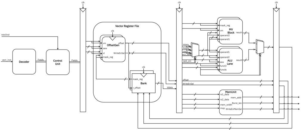
The image is a block diagram illustrating the architecture of a vector processing unit. It shows the flow of data and control signals between different components, including a decoder, control unit, vector register file, MV Block, ALU Lane, and memory unit. The diagram emphasizes the parallel processing capabilities inherent in vector operations.
### Components/Axes
* **Decoder:** Receives `vect_inst` as input and outputs `Fields`.
* **Control Unit:** Receives `newInst` and `Fields` as input and outputs `Fields`.
* **Vector Register File:** Contains `OffsetGen` and `Bank`.
* **OffsetGen:** Receives `vm`, `sew`, `vl`, and `mask_reg` as inputs and outputs `offset` and `WriteEnSel`.
* **Bank:** Receives `mask_reg` and `r_offset` as inputs and outputs `Vdata`.
* **MV Block:** Receives `mask_reg`, `vm`, `operand2`, and `operand1` as inputs and outputs `result`.
* **ALU Lane:** Receives `operand1`, `operand2`, `sew`, `funct3`, and `funct6` as inputs and outputs `result`.
* **MemUnit:** Receives `rs1_data`, `rs2_data`, `mem_width`, and `mop` as inputs and outputs `mem_addr` and `Burst_len` and `WriteEnMemSel`.
* **Data Signals:** `Vdata`, `Xdata`, `Idata`, `vs2 data`, `op1_src`, `offset`, `WriteEnSel`.
* **Clock Signals:** `clk` is present at multiple locations, indicating synchronous operation.
### Detailed Analysis
* **Decoder and Control Unit:** The decoder receives a vector instruction (`vect_inst`) and translates it into control signals (`Fields`) for the control unit. The control unit, in turn, generates further control signals based on the decoded instruction and a `newInst` signal.
* **Vector Register File:** This component stores vector data. It contains an `OffsetGen` block, which calculates memory offsets based on inputs like `vm`, `sew`, `vl`, and `mask_reg`. The `Bank` block likely represents the actual memory storage within the register file, receiving `mask_reg` and `r_offset` and outputting `Vdata`.
* **MV Block and ALU Lane:** These are the processing units. The MV Block performs vector operations, receiving operands and a mask (`mask_reg`) to selectively apply the operation. The ALU Lane performs arithmetic and logical operations, receiving operands, `sew` (likely specifying data width), and function codes (`funct3`, `funct6`).
* **MemUnit:** This unit handles memory access. It receives data addresses (`rs1_data`, `rs2_data`), memory width (`mem_width`), and operation codes (`mop`) to perform read/write operations. It outputs the memory address (`mem_addr`), burst length (`Burst_len`), and a write enable signal (`WriteEnMemSel`).
* **Data Flow:** Data flows from the Vector Register File to the MV Block and ALU Lane. The results from these units are then combined through a multiplexer before being sent to the MemUnit and back to the Vector Register File.
### Key Observations
* The diagram highlights the parallel nature of vector processing, with multiple data paths and processing units.
* The `mask_reg` signal is used in both the Vector Register File and the MV Block, indicating its importance in controlling vector operations.
* The presence of `clk` signals throughout the diagram suggests a synchronous design.
### Interpretation
The block diagram illustrates a typical architecture for a vector processing unit. The decoder and control unit handle instruction fetching and decoding, while the vector register file stores the vector data. The MV Block and ALU Lane perform the actual vector operations, and the MemUnit handles memory access. The use of masking and data width signals (`mask_reg`, `sew`) allows for flexible and efficient vector processing. The diagram emphasizes the parallel processing capabilities of the architecture, which are essential for achieving high performance in vector computations.