## Block Diagram: Memory System Architecture
### Overview
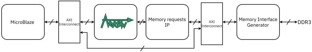
The image is a block diagram illustrating a memory system architecture. It shows the flow of data and control signals between different components, including a MicroBlaze processor, AXI interconnects, a memory requests IP block, a memory interface generator, and DDR3 memory.
### Components/Axes
* **MicroBlaze:** A processor block on the left.
* **AXI Interconnect:** Two blocks labeled "AXI Interconnect," one on either side of the "Memory requests IP" block.
* **Memory requests IP:** A block in the center labeled "Memory requests IP."
* **Memory Interface Generator:** A block on the right labeled "Memory Interface Generator."
* **DDR3:** A label on the far right, representing the DDR3 memory.
* **Arrows:** Arrows indicate the direction of data flow between the blocks. Double-headed arrows indicate bidirectional communication. A large, stylized green arrow is present within one of the blocks.
* **Slash Marks:** Slash marks on the arrows indicate multiple signals or a bus.
### Detailed Analysis or ### Content Details
1. **MicroBlaze to AXI Interconnect:** A bidirectional arrow connects the MicroBlaze processor to the first AXI Interconnect block.
2. **AXI Interconnect to Arrow Block:** A bidirectional arrow connects the first AXI Interconnect block to a block containing a stylized green arrow.
3. **Arrow Block to Memory requests IP:** A bidirectional arrow connects the arrow block to the "Memory requests IP" block.
4. **Memory requests IP to AXI Interconnect:** A bidirectional arrow connects the "Memory requests IP" block to the second AXI Interconnect block.
5. **AXI Interconnect to Memory Interface Generator:** A bidirectional arrow connects the second AXI Interconnect block to the "Memory Interface Generator" block.
6. **Memory Interface Generator to DDR3:** A bidirectional arrow connects the "Memory Interface Generator" block to the DDR3 memory.
7. **Feedback Loop:** A line connects the output of the first AXI Interconnect block back to the input of the "Memory requests IP" block, forming a feedback loop.
### Key Observations
* The diagram shows a typical memory system architecture with a processor, interconnects, memory controller, and memory.
* The AXI interconnects facilitate communication between the different components.
* The "Memory requests IP" block likely handles memory request arbitration and scheduling.
* The "Memory Interface Generator" block generates the necessary signals to interface with the DDR3 memory.
* The feedback loop suggests that the "Memory requests IP" block receives information from the AXI Interconnect, possibly related to memory access status or control signals.
### Interpretation
The diagram illustrates a memory system architecture commonly found in embedded systems. The MicroBlaze processor initiates memory requests, which are then routed through the AXI interconnect to the "Memory requests IP" block. This block likely manages the requests and forwards them to the "Memory Interface Generator," which translates the requests into the appropriate signals for the DDR3 memory. The feedback loop allows the "Memory requests IP" block to monitor the status of memory accesses and adjust its scheduling accordingly. The stylized arrow block is likely a placeholder for a more specific component or function within the memory system.