\n
## Diagram: Quantum Optical Circuit Schematics
### Overview
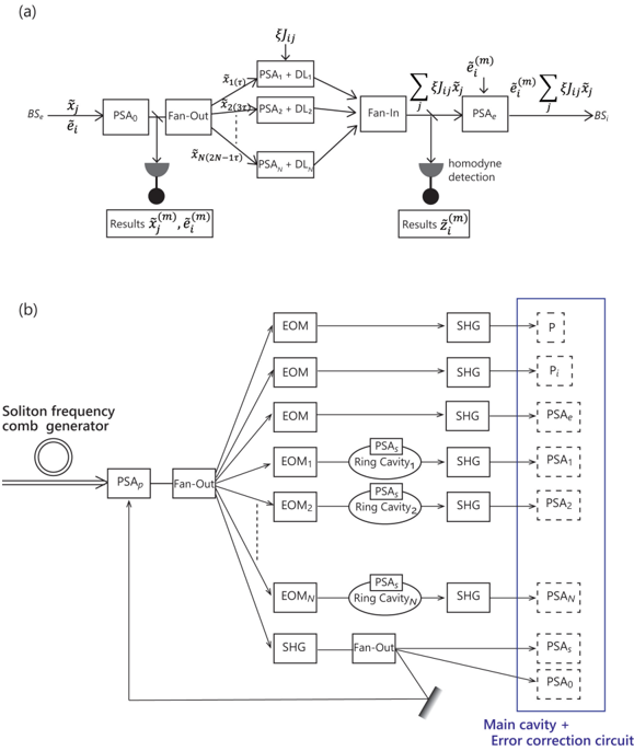
The image presents two schematic diagrams (labeled (a) and (b)) illustrating quantum optical circuits. Diagram (a) depicts a measurement scheme involving beam splitters (BS), phase-sensitive amplifiers (PSA), and fan-out elements. Diagram (b) illustrates a soliton frequency comb generator, utilizing electro-optic modulators (EOM), second harmonic generation (SHG), and ring cavities. Both diagrams use similar notation for optical components and signal flow.
### Components/Axes
**Diagram (a):**
* **Components:** BS (Beam Splitter), PSA (Phase-Sensitive Amplifier), DL (Delay Line), Fan-Out, Homodyne Detection.
* **Signals:** x̂ᵢ, êᵢ, x̂₁(m), ê¹(m), Σξj(x̂ᵢ), êᵢ(m), ξj(x̂ᵢ).
* **Labels:** "Results x̂ᵢ, êᵢ(m)", "Results êᵢ(m)".
**Diagram (b):**
* **Components:** PSA (Phase-Sensitive Amplifier), EOM (Electro-Optic Modulator), SHG (Second Harmonic Generation), Ring Cavity, Fan-Out.
* **Signals:** PSA<sub>D</sub>, x̂<sub>N</sub>, P<sub>i</sub>, PSA<sub>E</sub>, PSA<sub>1</sub>, PSA<sub>2</sub>, PSA<sub>N</sub>, PSA<sub>S</sub>, PSA<sub>0</sub>.
* **Labels:** "Soliton frequency comb generator", "Main cavity + Error correction circuit".
* **Ring Cavity Labels:** PSA<sub>1</sub> Ring Cavity<sub>1</sub>, PSA<sub>2</sub> Ring Cavity<sub>2</sub>, PSA<sub>N</sub> Ring Cavity<sub>N</sub>.
### Detailed Analysis or Content Details
**Diagram (a):**
The diagram shows a linear optical circuit. An input signal x̂ᵢ and êᵢ enters a beam splitter (BS<sub>c</sub>). The output is split via a Fan-Out element into multiple paths. Each path includes a phase-sensitive amplifier (PSA<sub>i</sub> + DL<sub>i</sub>) where 'i' ranges from 1 to N (2N-1 paths are shown). The outputs of these PSAs, x̂₁(m) and ê¹(m), are then combined using a Fan-In element. The combined signal is then fed into another PSA<sub>A</sub> and finally into a homodyne detection scheme, resulting in an output signal ξj(x̂ᵢ). The results of the measurement are labeled as x̂ᵢ and êᵢ(m).
**Diagram (b):**
The diagram depicts a more complex circuit. An input signal PSA<sub>D</sub> is split via a Fan-Out element into multiple paths. Each path contains an EOM (EOM<sub>1</sub> to EOM<sub>N</sub>), followed by a SHG stage. The output of each SHG stage is labeled P<sub>i</sub>, PSA<sub>E</sub>, PSA<sub>1</sub>, PSA<sub>2</sub>, and PSA<sub>N</sub>. These outputs are then fed into a "Main cavity + Error correction circuit" block. Within this block, there are multiple PSA stages (PSA<sub>S</sub>, PSA<sub>0</sub>) and dashed lines suggesting a feedback loop or iterative process. The ring cavities (PSA<sub>1</sub> Ring Cavity<sub>1</sub>, PSA<sub>2</sub> Ring Cavity<sub>2</sub>, PSA<sub>N</sub> Ring Cavity<sub>N</sub>) are positioned between the EOM/SHG stages and the main cavity.
### Key Observations
* Both diagrams utilize a consistent notation for optical components (boxes with labels) and signal flow (arrows).
* Diagram (b) is significantly more complex than diagram (a), suggesting a more sophisticated quantum optical process.
* The presence of ring cavities in diagram (b) indicates a resonant system, potentially used for frequency comb generation.
* The "Main cavity + Error correction circuit" in diagram (b) suggests a feedback mechanism for stabilizing or correcting the generated frequency comb.
* The use of phase-sensitive amplifiers (PSAs) in both diagrams indicates a focus on weak signal detection and amplification.
### Interpretation
Diagram (a) represents a basic quantum measurement scheme. The beam splitters and phase-sensitive amplifiers are used to perform homodyne detection, which allows for the measurement of quadrature components of the input signal. The multiple paths and fan-out/fan-in elements suggest a scheme for multi-mode or multi-channel measurement.
Diagram (b) illustrates a more advanced system for generating a soliton frequency comb. The EOMs modulate the input signal, and the SHG stages convert the signal to higher frequencies. The ring cavities provide a resonant structure for enhancing the comb generation process. The main cavity and error correction circuit likely stabilize the comb and correct for any imperfections.
The combination of these two diagrams suggests a potential application where a soliton frequency comb is generated and then measured using a homodyne detection scheme. This could be used for high-precision spectroscopy, optical metrology, or quantum communication. The error correction circuit in diagram (b) is crucial for maintaining the coherence and stability of the frequency comb, which is essential for these applications. The dashed lines in the main cavity suggest an iterative process, potentially for optimizing the comb parameters or correcting for noise.