TECHNICAL ASSET FINGERPRINT
1ed335402f9f1d587db1e6ec
Click to view fullscreen
Press ESC or click to close
FOUND IN PAPERS
EXPERT: healer-alpha-free VERSION 1
RUNTIME: free/openrouter/healer-alpha
INTEL_VERIFIED
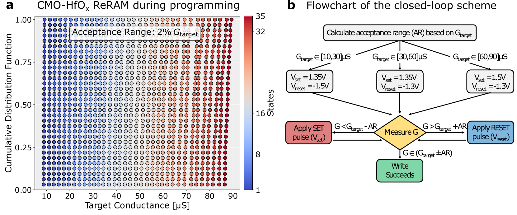
## [Chart/Diagram Type]: Composite Technical Figure (Scatter Plot and Flowchart)
### Overview
The image is a two-part technical figure labeled **a** and **b**. Part **a** is a scatter plot visualizing the programming distribution of a CMO-HfOₓ ReRAM device. Part **b** is a flowchart detailing the closed-loop algorithm used to program the device to a target conductance. The overall purpose is to illustrate the precision and methodology of a conductance programming scheme for resistive memory.
### Components/Axes
**Part a: CMO-HfOₓ ReRAM during programming**
* **Chart Type:** Scatter plot with a color-coded third dimension.
* **X-Axis:** Labeled "Target Conductance [µS]". The scale runs linearly from 10 to 90 µS, with major tick marks every 10 µS.
* **Y-Axis:** Labeled "Cumulative Distribution Function". The scale runs linearly from 0.00 to 1.00, with major tick marks every 0.25.
* **Data Representation:** Data points are arranged in vertical columns, each corresponding to a specific target conductance value on the x-axis. Each column contains multiple dots stacked vertically, representing the distribution of achieved conductance states for that target.
* **Color Legend (States):** A vertical color bar is positioned to the right of the plot. It is labeled "States" and has a scale from 1 (bottom, blue) to 35 (top, red). The gradient transitions from dark blue (low state count) through light blue, white, orange, to dark red (high state count).
* **Annotation:** A text box in the upper-left quadrant of the plot area states: "Acceptance Range: 2% G_target".
**Part b: Flowchart of the closed-loop scheme**
* **Chart Type:** Process flowchart.
* **Title:** "Flowchart of the closed-loop scheme".
* **Components & Flow:**
1. **Start (Top Rectangle):** "Calculate acceptance range (AR) based on G_target".
2. **Decision Branches (Three Paths):** Based on the value of G_target:
* Left Path: `G_target ∈ [10,30]µS` → Leads to a rectangle with `V_set = 1.35V`, `V_reset = -1.5V`.
* Middle Path: `G_target ∈ [30,60]µS` → Leads to a rectangle with `V_set = 1.35V`, `V_reset = -1.3V`.
* Right Path: `G_target ∈ [60,90]µS` → Leads to a rectangle with `V_set = 1.5V`, `V_reset = -1.3V`.
3. **Convergence Point (Diamond):** All three paths lead to a central yellow diamond labeled "Measure G".
4. **Feedback Loops from Diamond:**
* **Left Arrow (Pink Rectangle):** Condition `G < G_target - AR` → Action "Apply SET pulse (V_set)".
* **Right Arrow (Blue Rectangle):** Condition `G > G_target + AR` → Action "Apply RESET pulse (V_reset)".
* **Down Arrow (Green Rectangle):** Condition `G ∈ (G_target ± AR)` → Outcome "Write Succeeds".
5. **Loop Closure:** The "Apply SET pulse" and "Apply RESET pulse" actions both have arrows pointing back to the "Measure G" diamond, creating a closed-loop feedback system.
### Detailed Analysis
**Part a: Data Distribution**
* **Trend Verification:** For each vertical column (fixed target conductance), the data points (dots) are distributed along the y-axis (Cumulative Distribution Function). The color of the dots changes systematically from left to right across the plot.
* **Spatial Grounding & Data Points:**
* At low target conductance (e.g., 10 µS), the column of dots is predominantly **blue**, indicating a low number of states (approximately 1-8 according to the color bar).
* As target conductance increases (moving right along the x-axis), the color of the dots in each column shifts progressively through light blue, white, and orange.
* At high target conductance (e.g., 80-90 µS), the columns are predominantly **red**, indicating a high number of states (approximately 25-35).
* The vertical spread (CDF range) of dots within each column appears relatively consistent across different target conductance values, suggesting a similar distribution shape, but the *number* of distinct conductance levels (states) achievable increases with the target value.
**Part b: Process Logic**
* The flowchart defines a precise, adaptive programming algorithm.
* The **Acceptance Range (AR)** is a critical parameter, defined as 2% of the target conductance (G_target), as noted in part **a**.
* The algorithm uses different programming voltages (`V_set`, `V_reset`) depending on the target conductance range, indicating that the device's response is non-linear and requires calibration.
* The core is an iterative **measure-and-adjust** loop: measure conductance (G), compare it to the target window (`G_target ± AR`), and apply a corrective pulse (SET to increase conductance, RESET to decrease it) until the measured value falls within the acceptance range.
### Key Observations
1. **State Density vs. Target:** There is a clear positive correlation between the target conductance and the number of distinguishable states the device can be programmed to. Higher conductance targets allow for a finer or more numerous set of intermediate states.
2. **Adaptive Voltage Control:** The programming scheme is not one-size-fits-all. It employs three distinct voltage profiles tailored to low, medium, and high conductance regimes, likely to optimize programming speed, accuracy, or device endurance.
3. **Tight Tolerance:** The acceptance range of 2% indicates a high-precision programming requirement, necessitating the closed-loop feedback system shown in the flowchart.
4. **Visual Confirmation:** The scatter plot in **a** visually demonstrates the *result* of the process described in **b**. The tight vertical clustering of dots (within the CDF) for each target value is evidence of the algorithm's success in keeping the final conductance within a narrow band around the target.
### Interpretation
This figure collectively demonstrates a sophisticated method for analog programming of a ReRAM device. The data in **a** shows that the device can be reliably placed into multiple conductance states, with the number of available states scaling with the target conductance level. This is crucial for applications like neuromorphic computing, where synaptic weights are represented by conductance values.
The flowchart in **b** reveals the "how": a deterministic, feedback-controlled algorithm that compensates for device variability by iteratively measuring and adjusting. The use of different voltages for different conductance ranges suggests an underlying physical model of the device's switching behavior is being used to improve efficiency. The 2% acceptance range is a key performance metric, indicating the system's precision.
**Peircean Investigation:** The sign (the image) represents an **icon** of the device's behavior (the distribution of states) and an **index** of the causal process (the algorithm) that produces that behavior. The correlation between higher target conductance and more states (red dots) is an iconic representation of increased analog capacity. The flowchart is an indexical map, pointing directly to the sequence of operations (calculate, measure, pulse) that must occur to achieve the result shown in the plot. The outlier would be any column in the plot with a color inconsistent with its neighbors (e.g., a red column at 20 µS), which would indicate a breakdown in the assumed relationship or a measurement error, but none are apparent. The system is designed for predictable, analog storage.
DECODING INTELLIGENCE...