\n
## Chart: PCM Response Over Time
### Overview
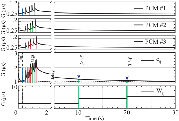
The image presents a time-domain plot showing the response of three Phase Change Memory (PCM) devices (PCM #1, PCM #2, PCM #3) and a combined signal (e<sub>ij</sub>) alongside a write pulse (W<sub>ij</sub>). The plot displays the change in 'G' (likely conductance or a related property) in microseconds (µs) over time in seconds (s). The chart aims to illustrate the dynamic behavior of PCM devices during read and write operations.
### Components/Axes
* **X-axis:** Time (s), ranging from 0 to 30 seconds.
* **Y-axis:** G (µs), with varying scales for each subplot.
* PCM #1, PCM #2, PCM #3: Scale from 0 to 1.2E+6 µs (1.2 million µs).
* e<sub>ij</sub>: Scale from 0 to 3 µs.
* W<sub>ij</sub>: Scale from 0 to 10 µs.
* **Data Series:**
* PCM #1 (Black line)
* PCM #2 (Green line)
* PCM #3 (Red line)
* e<sub>ij</sub> (Black line)
* W<sub>ij</sub> (Green line)
* **Annotations:**
* "init." (initialization)
* "tags"
* "delay"
* "3rd-f" (appears twice, indicating a third frequency component or a related event)
* **Legend:** Located on the right side of the chart, labeling each data series with its corresponding color.
### Detailed Analysis
The chart consists of five subplots stacked vertically.
* **PCM #1:** The black line shows an initial rapid decrease in G, followed by a slow decay towards a stable value around 0.25 µs. The initial drop occurs within approximately 0.5 seconds.
* **PCM #2:** The green line exhibits a similar initial drop in G, but with a more pronounced oscillation before settling around 0.25 µs. The initial drop occurs within approximately 0.5 seconds.
* **PCM #3:** The red line shows a similar initial drop in G, but with a more pronounced oscillation before settling around 0.25 µs. The initial drop occurs within approximately 0.5 seconds.
* **e<sub>ij</sub>:** The black line shows a complex response. Initially, all three PCM responses (black, green, and red) overlap. After approximately 2 seconds, the signal decays, with a noticeable "delay" indicated by an arrow. Around 10 seconds and 20 seconds, there are spikes labeled "3rd-f". The signal stabilizes around 1 µs.
* **W<sub>ij</sub>:** The green line represents a write pulse, consisting of rectangular pulses with a duration of approximately 2 seconds, repeated at intervals of approximately 8 seconds. The amplitude of the pulse is around 10 µs.
**Approximate Data Points (from visual inspection):**
* **PCM #1:** At t=0s, G ≈ 1.2 µs. At t=0.5s, G ≈ 0.3 µs. At t=30s, G ≈ 0.25 µs.
* **PCM #2:** At t=0s, G ≈ 1.2 µs. At t=0.5s, G ≈ 0.3 µs. At t=30s, G ≈ 0.25 µs.
* **PCM #3:** At t=0s, G ≈ 1.2 µs. At t=0.5s, G ≈ 0.3 µs. At t=30s, G ≈ 0.25 µs.
* **e<sub>ij</sub>:** At t=0s, G ≈ 2 µs. At t=2s, G ≈ 1.2 µs. At t=10s, G ≈ 1.1 µs. At t=20s, G ≈ 1.1 µs.
* **W<sub>ij</sub>:** Pulse amplitude ≈ 10 µs. Pulse width ≈ 2s. Period ≈ 10s.
### Key Observations
* All three PCM devices exhibit a similar initial response, suggesting a common underlying physical mechanism.
* The "e<sub>ij</sub>" signal appears to be a composite of the responses from the three PCM devices.
* The write pulse (W<sub>ij</sub>) is significantly larger in amplitude than the read signal (e<sub>ij</sub>).
* The "3rd-f" spikes in the "e<sub>ij</sub>" signal may indicate a resonant frequency or a harmonic component in the system.
* The delay between the initial response and the stabilization of the "e<sub>ij</sub>" signal suggests a latency in the measurement or the PCM device itself.
### Interpretation
This chart demonstrates the dynamic behavior of PCM devices during read and write operations. The initial rapid decrease in conductance (G) represents the transition of the PCM material from a crystalline to an amorphous state during a write operation. The subsequent decay and stabilization of G represent the relaxation of the material and the establishment of a new resistance state. The "e<sub>ij</sub>" signal likely represents the read signal, which is used to sense the resistance state of the PCM device. The write pulse (W<sub>ij</sub>) is used to induce the change in resistance state.
The overlapping initial responses of the three PCM devices suggest that they are responding to the same stimulus. The differences in the subsequent behavior may be due to variations in the manufacturing process or the operating conditions of the devices. The "3rd-f" spikes in the "e<sub>ij</sub>" signal may be related to the resonant frequency of the PCM device or the measurement circuitry. The delay between the initial response and the stabilization of the "e<sub>ij</sub>" signal may be due to the time it takes for the PCM material to fully transition to its new resistance state.
The chart provides valuable insights into the performance characteristics of PCM devices and can be used to optimize their design and operation. The observed trends and anomalies may indicate potential areas for improvement in the manufacturing process or the control circuitry.