## Integrated Circuit Layouts
### Overview
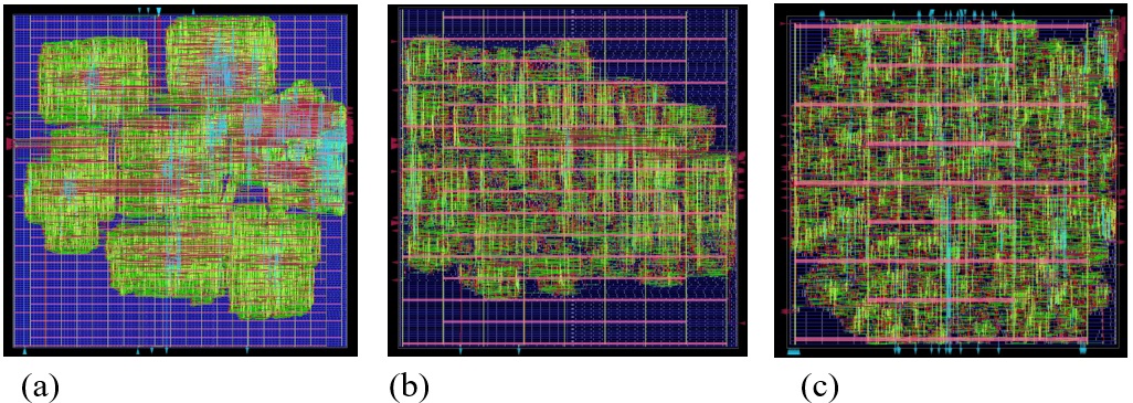
The image presents three different layouts of integrated circuits, labeled (a), (b), and (c). Each layout shows a complex arrangement of interconnected components and wiring on a grid-based background. The layouts differ in their overall structure and component density.
### Components/Axes
* **Grid Background:** A blue grid provides a spatial reference for the layout.
* **Components:** Represented by green and other colored shapes, indicating different functional blocks or circuit elements.
* **Wiring:** Red, light blue, and other colored lines represent the interconnections between components.
* **Labels:** The layouts are labeled (a), (b), and (c) at the bottom.
### Detailed Analysis or ### Content Details
**Layout (a):**
* The layout is organized into several distinct clusters or blocks of components.
* The clusters are interconnected by a network of wiring.
* The wiring density appears to be higher within the clusters than between them.
* The layout is not uniform, with some areas having a higher concentration of components than others.
* There are several red triangles along the left edge of the layout.
**Layout (b):**
* The layout is more uniformly distributed compared to layout (a).
* The components are arranged in a more regular pattern.
* There are horizontal red lines that appear to be power or ground rails.
* The wiring density is relatively consistent across the layout.
* There are several red triangles along the left edge of the layout.
**Layout (c):**
* Similar to layout (b), the components are arranged in a relatively uniform pattern.
* There are horizontal red lines that appear to be power or ground rails.
* The wiring density is relatively consistent across the layout.
* There are several light blue triangles along the top edge of the layout.
### Key Observations
* Layout (a) has a clustered structure, while layouts (b) and (c) have a more uniform structure.
* The wiring density varies across the layouts, with layout (a) having higher density within the clusters.
* The red lines in layouts (b) and (c) suggest a structured power or ground distribution network.
### Interpretation
The image shows different approaches to integrated circuit layout. Layout (a) might represent a design where functional blocks are physically grouped together, while layouts (b) and (c) might represent designs optimized for uniform component distribution and power delivery. The differences in layout structure can impact performance, power consumption, and manufacturability of the integrated circuit. The red triangles along the edges of layouts (a) and (b), and the light blue triangles along the top edge of layout (c) might be alignment marks or test points.