\n
## Diagram: Memory Cell Circuit and State Diagram
### Overview
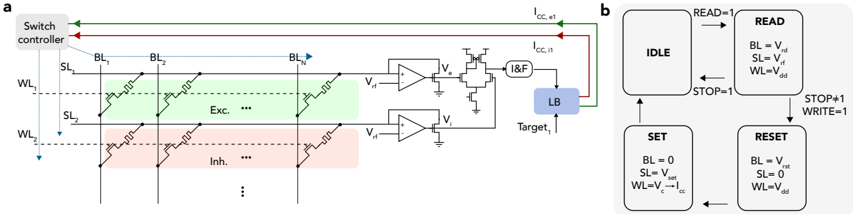
The image presents a schematic diagram of a memory cell circuit (labeled 'a') alongside a state diagram illustrating its operational modes (labeled 'b'). The circuit appears to be a non-volatile memory cell, likely a resistive RAM (ReRAM) or similar technology, with excitation (Exc.) and inhibition (Inh.) phases. The state diagram shows the transitions between IDLE, READ, SET, and RESET states.
### Components/Axes
**Part a (Circuit Diagram):**
* **Switch Controller:** Green arrow indicating control signals.
* **BL:** Bit Line (two instances, labeled BL and BL̅)
* **SL:** Select Line (two instances, labeled SL and SL̅)
* **WL:** Word Line (two instances, labeled WL and WL̅)
* **V<sub>T</sub>:** Threshold Voltage (two instances)
* **cc, v1:** Positive supply voltage.
* **cc, n:** Negative supply voltage.
* **LB:** Load Balance (blue oval)
* **Target:** Output signal.
* **&F:** AND/Flip-Flop gate.
* **Exc.:** Excitation region (highlighted in green).
* **Inh.:** Inhibition region (highlighted in red).
* **Dotted Lines:** Represent continuation of the memory array.
**Part b (State Diagram):**
* **IDLE:** Initial state.
* **READ:** State for reading the memory cell value.
* **SET:** State for setting the memory cell to a high resistance state.
* **RESET:** State for resetting the memory cell to a low resistance state.
* **READ = 1:** Transition from IDLE to READ.
* **STOP = 1:** Transition from IDLE to SET.
* **STOP + 1 WRITE = 1:** Transition from IDLE to RESET.
* **BL = V<sub>T</sub>, SL = V<sub>T</sub>, WL = V<sub>W</sub>:** Conditions for READ state.
* **BL = 0, SL = V<sub>T</sub>, WL = V<sub>SET</sub>:** Conditions for SET state.
* **BL = V<sub>T</sub>, SL = 0, WL = V<sub>RESET</sub>:** Conditions for RESET state.
### Detailed Analysis or Content Details
**Part a (Circuit Diagram):**
The circuit consists of two parallel memory cells, each with a bit line (BL/BL̅), select line (SL/SL̅), and word line (WL/WL̅). The excitation region (Exc.) shows a series of pulses applied to the word lines, while the inhibition region (Inh.) shows a similar pattern. The bit lines are connected to a differential amplifier and an AND/Flip-Flop gate. The Load Balance (LB) signal is connected to the output. The circuit utilizes complementary signals (BL/BL̅, SL/SL̅, WL/WL̅) for operation.
**Part b (State Diagram):**
The state diagram shows a four-state machine.
* From IDLE, the system transitions to READ upon receiving a READ signal (READ = 1).
* From IDLE, the system transitions to SET upon receiving a STOP signal (STOP = 1).
* From IDLE, the system transitions to RESET upon receiving a STOP + 1 WRITE signal.
* The READ state is defined by BL = V<sub>T</sub>, SL = V<sub>T</sub>, and WL = V<sub>W</sub>.
* The SET state is defined by BL = 0, SL = V<sub>T</sub>, and WL = V<sub>SET</sub>.
* The RESET state is defined by BL = V<sub>T</sub>, SL = 0, and WL = V<sub>RESET</sub>.
### Key Observations
* The circuit utilizes a differential sensing scheme with the differential amplifier.
* The excitation and inhibition regions suggest a pulse-based operation for programming the memory cell.
* The state diagram clearly defines the conditions for each operation (READ, SET, RESET).
* The use of complementary signals (BL/BL̅, SL/SL̅, WL/WL̅) indicates a balanced circuit design.
* The Load Balance (LB) signal suggests a mechanism for stabilizing the memory cell operation.
### Interpretation
The diagram illustrates a memory cell architecture that leverages resistive switching behavior. The excitation and inhibition phases likely control the resistance state of the memory cell, allowing it to store information. The state diagram provides a clear understanding of the control signals and conditions required for each operation. The differential sensing scheme enhances the reliability of the read operation. The Load Balance signal is likely used to compensate for process variations and improve the overall performance of the memory cell. The circuit appears to be designed for non-volatile memory applications, where data retention is crucial. The use of pulses for excitation and inhibition suggests a potential for fine-grained control over the memory cell's resistance state, enabling multi-level cell (MLC) operation. The diagram suggests a robust and efficient memory cell design with a clear operational flow.