## Circuit Diagram & Performance Characterization: Neuromorphic Computing System
### Overview
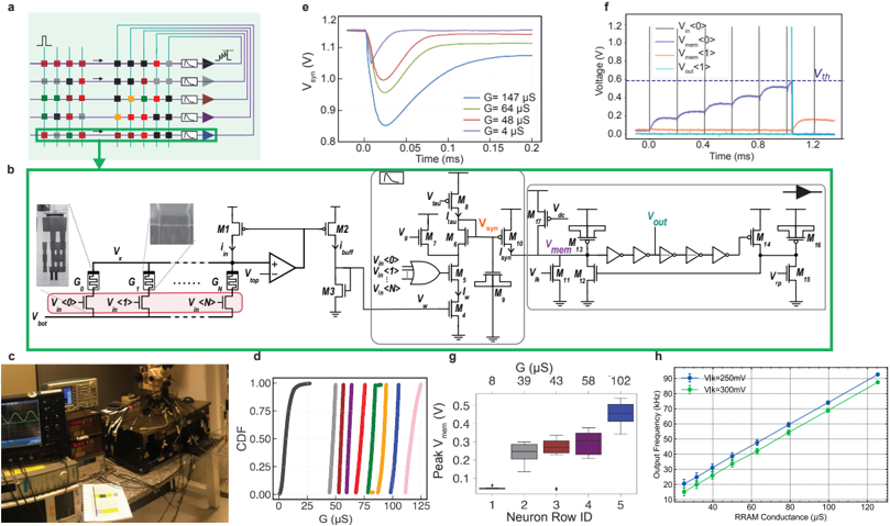
The image presents a combination of a circuit diagram, experimental setup photograph, and performance characterization graphs related to a neuromorphic computing system. The system appears to be based on resistive random-access memory (RRAM) and utilizes a chain of inverters to implement neuron and synapse functionality. The image details the circuit architecture, experimental setup, and the relationship between RRAM conductance and the resulting output frequency.
### Components/Axes
The image is divided into several sub-sections:
* **(a):** Chain of inverters representing a neuron circuit.
* **(b):** Detailed schematic of the neuron circuit with RRAM elements.
* **(c):** Photograph of the experimental setup, including hardware and monitoring equipment.
* **(d):** Cumulative Distribution Function (CDF) of RRAM conductance (G). X-axis: G (µs), Y-axis: CDF (0.00 - 1.00).
* **(e):** Simulation of input voltage (V<sub>in</sub>) over time for different RRAM conductance values. X-axis: Time (ms), Y-axis: V<sub>in</sub> (V).
* **(f):** Voltage waveform showing the output of the inverter chain for different input voltages. X-axis: Time (ms), Y-axis: Voltage (V).
* **(g):** Box plot of peak output voltage (V<sub>peak</sub>) for different neuron row IDs. X-axis: Neuron Row ID (1-5), Y-axis: V<sub>peak</sub> (V).
* **(h):** Output frequency versus RRAM conductance. X-axis: RRAM Conductance (µs), Y-axis: Output Frequency (kHz). Two lines are shown for different input voltages (V<sub>in</sub> = 250mV and V<sub>in</sub> = 300mV).
### Detailed Analysis or Content Details
**(a) Inverter Chain:**
A series of inverters are shown, with input signals propagating from left to right. The input signal is a square wave.
**(b) Neuron Circuit Schematic:**
The schematic shows transistors (M1, M2, M3, etc.) and RRAM devices. The RRAM devices are labeled with conductance values (G). The schematic includes voltage sources (V<sub>in</sub>, V<sub>dd</sub>, V<sub>ss</sub>) and an output (V<sub>out</sub>).
**(c) Experimental Setup:**
The photograph shows a rack of electronic equipment, including a computer monitor displaying waveforms, and a circuit board with the neuromorphic chip.
**(d) CDF of RRAM Conductance:**
The CDF shows the distribution of RRAM conductance values. Multiple curves are plotted, each representing a different RRAM device. The conductance values range from approximately 25 µs to 125 µs. The CDF indicates that the conductance values are not uniformly distributed.
**(e) Input Voltage Simulation:**
The graph shows the simulated input voltage (V<sub>in</sub>) over time for different RRAM conductance values (G = 147 µs, 64 µs, 48 µs, 4 µs). The curves show that higher conductance values result in faster voltage transitions. The Y-axis ranges from approximately 0.9V to 1.2V. The X-axis ranges from 0.0 to 0.25 ms.
**(f) Voltage Waveform:**
The graph shows the output voltage waveform for different input voltages (V<sub><0</sub>, V<sub><1</sub>, V<sub><2</sub>, V<sub><3</sub>). The waveform shows a delayed and inverted signal. The Y-axis ranges from 0.0 to 1.0V. The X-axis ranges from 0.0 to 1.2 ms.
**(g) Peak Output Voltage:**
The box plot shows the distribution of peak output voltages (V<sub>peak</sub>) for different neuron row IDs (1-5). Neuron row ID 4 has the highest median V<sub>peak</sub>, approximately 0.35V. Neuron row ID 1 has the lowest median V<sub>peak</sub>, approximately 0.15V. The Y-axis ranges from 0.0 to 0.4V.
**(h) Output Frequency vs. Conductance:**
The graph shows the relationship between output frequency and RRAM conductance for two different input voltages (V<sub>in</sub> = 250mV and V<sub>in</sub> = 300mV). Both lines show an upward trend, indicating that higher conductance values result in higher output frequencies. The line for V<sub>in</sub> = 300mV is consistently above the line for V<sub>in</sub> = 250mV. At a conductance of 40 µs, the output frequency is approximately 10 kHz for V<sub>in</sub> = 250mV and approximately 20 kHz for V<sub>in</sub> = 300mV. At a conductance of 120 µs, the output frequency is approximately 60 kHz for V<sub>in</sub> = 250mV and approximately 80 kHz for V<sub>in</sub> = 300mV.
### Key Observations
* The CDF of RRAM conductance (d) shows a non-uniform distribution, suggesting variability in the RRAM devices.
* Higher RRAM conductance values lead to faster voltage transitions in the simulation (e).
* The output frequency increases with RRAM conductance (h), demonstrating the synaptic weight effect.
* Neuron row ID 4 exhibits the highest peak output voltage (g).
* Increasing the input voltage (V<sub>in</sub>) increases the output frequency (h).
### Interpretation
The image demonstrates a neuromorphic computing system based on RRAM synapses and inverter-based neurons. The RRAM conductance acts as a synaptic weight, modulating the output frequency of the neuron. The simulation and experimental results confirm that higher conductance values lead to higher output frequencies, mimicking the behavior of biological synapses. The variability in RRAM conductance, as shown by the CDF, could impact the performance and reliability of the system. The differences in peak output voltage between neuron rows suggest variations in device characteristics or circuit layout. The system's ability to modulate output frequency based on conductance provides a foundation for implementing complex neural networks. The experimental setup photograph provides context for the research and development of this neuromorphic system. The data suggests a functional neuromorphic system, but further characterization and optimization are needed to address the variability in RRAM devices and improve overall performance.