TECHNICAL ASSET FINGERPRINT
3b91b885986544946ad416bc
Click to view fullscreen
Press ESC or click to close
FOUND IN PAPERS
EXPERT: healer-alpha-free VERSION 1
RUNTIME: free/openrouter/healer-alpha
INTEL_VERIFIED
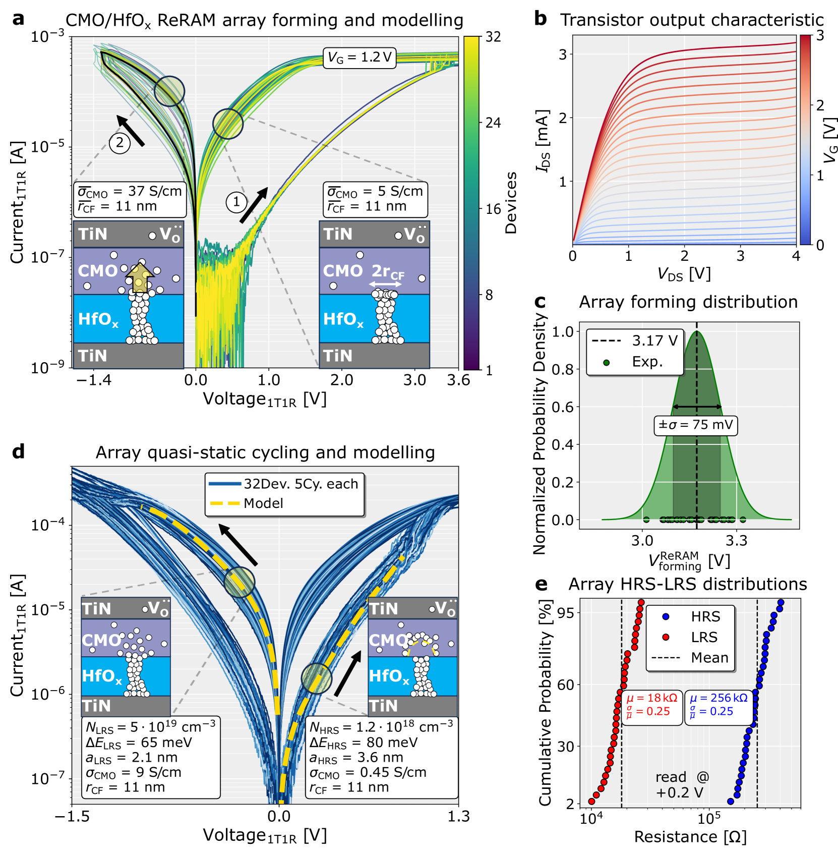
## Multi-Panel Technical Figure: CMO/HfOₓ ReRAM Array Characterization
### Overview
This image is a composite figure containing five subplots (labeled **a** through **e**) that present electrical characterization data and modeling results for a CMO/HfOₓ Resistive Random-Access Memory (ReRAM) array integrated with a transistor (1T1R structure). The data covers the initial forming process, transistor characteristics, cycling behavior, and statistical distributions of key parameters.
### Components/Axes
The figure is divided into five distinct panels:
* **Panel a (Top Left):** A current-voltage (I-V) plot titled "CMO/HfOₓ ReRAM array forming and modelling".
* **Panel b (Top Right):** A transistor output characteristic plot.
* **Panel c (Middle Right):** A probability density plot titled "Array forming distribution".
* **Panel d (Bottom Left):** A current-voltage (I-V) plot titled "Array quasi-static cycling and modelling".
* **Panel e (Bottom Right):** A cumulative probability plot titled "Array HRS-LRS distributions".
### Detailed Analysis
#### **Panel a: CMO/HfOₓ ReRAM array forming and modelling**
* **Chart Type:** Current-Voltage (I-V) characteristic on a semi-logarithmic scale.
* **Axes:**
* **Y-axis:** `Current_1T1R [A]` (log scale, ranging from 10⁻⁹ to 10⁻³ A).
* **X-axis:** `Voltage_1T1R [V]` (linear scale, ranging from -1.4 to 3.6 V).
* **Data Series & Legend:**
* Multiple colored lines represent I-V curves for different devices.
* A vertical color bar on the right, labeled `Devices`, maps line color to device number (1 to 32). Yellow/green lines correspond to higher device numbers, blue/purple to lower numbers.
* **Annotations & Insets:**
* A text box in the upper right states `V_G = 1.2 V`, indicating the gate voltage applied to the transistor during measurement.
* Two schematic insets depict the device structure (TiN/CMO/HfOₓ/TiN) before and after forming.
* **Left Inset (Pre-forming):** Labeled with parameters `σ_CMO = 37 S/cm` and `r_CF = 11 nm`. It shows a narrow conductive filament (CF) beginning to form in the HfOₓ layer.
* **Right Inset (Post-forming):** Labeled with parameters `σ_CMO = 5 S/cm` and `r_CF = 11 nm`. It shows a wider conductive filament (`2r_CF`).
* Black arrows labeled `①` and `②` indicate the direction of the voltage sweep during the forming process (from 0V to positive voltage, then back).
* Two gray circles highlight regions of interest on the curves, likely indicating the onset of forming and the high-current state.
* **Trend:** All devices show a sharp increase in current (forming event) at a positive voltage between approximately 2.5V and 3.5V. The current then saturates at a high level (~10⁻³ A) as the voltage is swept back.
#### **Panel b: Transistor output characteristic**
* **Chart Type:** Family of curves for a transistor.
* **Axes:**
* **Y-axis:** `I_DS [mA]` (linear scale, 0 to 3 mA).
* **X-axis:** `V_DS [V]` (linear scale, 0 to 4 V).
* **Data Series & Legend:**
* Multiple lines, color-coded by gate voltage (`V_G`).
* A vertical color bar on the right, labeled `V_G [V]`, maps line color to gate voltage (0V to 3V). Blue lines are low V_G, red lines are high V_G.
* **Trend:** For a fixed V_G, drain-source current (`I_DS`) increases with `V_DS` and then saturates. For a fixed `V_DS`, `I_DS` increases significantly with increasing `V_G`.
#### **Panel c: Array forming distribution**
* **Chart Type:** Normalized probability density function (histogram with fitted curve).
* **Axes:**
* **Y-axis:** `Normalized Probability Density` (linear scale, 0.0 to 1.0).
* **X-axis:** `V_forming^ReRAM [V]` (linear scale, ~2.9V to 3.4V).
* **Data Series & Legend:**
* Green dots (`Exp.`) represent experimental data points for the forming voltage of individual devices.
* A dashed vertical line marks the mean forming voltage at `3.17 V`.
* A solid green curve represents a Gaussian fit to the data.
* **Annotations:**
* A text box indicates the standard deviation: `±σ = 75 mV`.
* **Distribution:** The forming voltages are normally distributed around a mean of 3.17V with a standard deviation of 75mV.
#### **Panel d: Array quasi-static cycling and modelling**
* **Chart Type:** Current-Voltage (I-V) characteristic on a semi-logarithmic scale.
* **Axes:**
* **Y-axis:** `Current_1T1R [A]` (log scale, 10⁻⁷ to 10⁻⁴ A).
* **X-axis:** `Voltage_1T1R [V]` (linear scale, -1.5V to 1.3V).
* **Data Series & Legend:**
* A legend in the top center identifies:
* `32Dev. 5Cy. each`: Blue lines represent experimental I-V data from 32 devices, each cycled 5 times.
* `Model`: A yellow dashed line represents the simulation/model fit.
* **Annotations & Insets:**
* Two schematic insets depict the device structure in Low Resistance State (LRS) and High Resistance State (HRS).
* **Left Inset (LRS):** Lists parameters: `N_LRS = 5·10¹⁹ cm⁻³`, `ΔE_LRS = 65 meV`, `a_LRS = 2.1 nm`, `σ_CMO = 9 S/cm`, `r_CF = 11 nm`.
* **Right Inset (HRS):** Lists parameters: `N_HRS = 1.2·10¹⁸ cm⁻³`, `ΔE_HRS = 80 meV`, `a_HRS = 3.6 nm`, `σ_CMO = 0.45 S/cm`, `r_CF = 11 nm`.
* Black arrows indicate the bipolar switching direction: positive voltage for SET (HRS to LRS), negative voltage for RESET (LRS to HRS).
* Gray circles highlight the SET and RESET transition regions on the curves.
* **Trend:** The device exhibits clear bipolar resistive switching. The model (yellow dashed line) closely follows the average behavior of the experimental data (blue lines).
#### **Panel e: Array HRS-LRS distributions**
* **Chart Type:** Cumulative probability plot.
* **Axes:**
* **Y-axis:** `Cumulative Probability [%]` (linear scale, 2% to 95%).
* **X-axis:** `Resistance [Ω]` (log scale, 10⁴ to ~5·10⁵ Ω).
* **Data Series & Legend:**
* A legend identifies:
* `HRS`: Blue dots.
* `LRS`: Red dots.
* `Mean`: Dashed vertical lines.
* **Annotations:**
* Text boxes provide statistical parameters for each state:
* **LRS (Red):** `μ = 18 kΩ`, `σ/μ = 0.25`.
* **HRS (Blue):** `μ = 256 kΩ`, `σ/μ = 0.25`.
* A label at the bottom states `read @ +0.2 V`, indicating the resistance was measured at a read voltage of 0.2V.
* **Distribution:** The LRS and HRS resistance values form two distinct, well-separated distributions. Both have a relative standard deviation (σ/μ) of 0.25, indicating similar variability. The HRS mean is approximately 14 times higher than the LRS mean.
### Key Observations
1. **Forming Process (Panel a & c):** The initial electroforming of the ReRAM devices is a stochastic process with a relatively tight distribution (σ = 75 mV around 3.17 V).
2. **Transistor Control (Panel b):** The transistor provides effective current compliance and control, as seen by the well-behaved output characteristics.
3. **Bipolar Switching (Panel d):** The devices exhibit robust and repeatable bipolar switching behavior over multiple cycles, which is well-captured by the physical model.
4. **State Separation (Panel e):** There is a clear and significant resistance window between the HRS (~256 kΩ) and LRS (~18 kΩ), which is crucial for memory readout. The variability (σ/μ = 0.25) is consistent across both states.
5. **Model Agreement (Panel d):** The physical model, using parameters related to oxygen vacancy concentration (`N`), activation energy (`ΔE`), and filament geometry (`a`, `r_CF`), accurately reproduces the experimental switching curves.
### Interpretation
This figure provides a comprehensive electrical and physical analysis of a CMO/HfOₓ ReRAM array. The data demonstrates the fundamental functionality of the memory cells: a one-time forming step creates a conductive filament, after which the device can be reliably switched between a high and low resistance state using bipolar voltage pulses.
The **forming distribution (c)** is critical for circuit design, as it defines the voltage margin required to initialize all cells in an array. The **transistor characteristics (b)** confirm its suitability as a selection and current-limiting element. The **cycling data and model (d)** reveal the underlying physics of switching, linking electrical behavior to changes in the conductive filament's properties (e.g., vacancy concentration and effective radius). Finally, the **resistance distributions (e)** quantify the memory window and variability, which are key metrics for determining the reliability and potential density of a memory technology. The consistent relative variability (σ/μ) in both states suggests a common physical origin for the fluctuations, likely related to the atomic-scale nature of the conductive filament.
DECODING INTELLIGENCE...