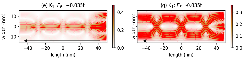
# Technical Data Extraction: Current Density Streamline Plots
This document provides a detailed extraction of the data and components from the provided image, which consists of two side-by-side scientific plots (labeled 'e' and 'g') representing current density distributions in a nanostructure.
## 1. Global Image Metadata
* **Language:** English
* **Subject Matter:** Physics/Nanotechnology (likely Graphene or 2D materials research).
* **Visual Format:** Heatmaps with overlaid vector streamlines.
* **Coordinate System:** Cartesian coordinates representing physical dimensions in nanometers (nm).
---
## 2. Component Isolation: Plot (e)
### Header Information
* **Label:** (e)
* **Title String:** $K_1: E_F = +0.035t$
* **Interpretation:** This represents the $K_1$ valley with a positive Fermi energy ($E_F$) of $0.035t$.
### Axis and Scale
* **Y-axis Label:** width (nm)
* **Y-axis Markers:** -10, 0, 10
* **X-axis Label:** length (nm)
* **X-axis Markers:** -40, -20, 0, 20, 40
* **Color Bar (Legend):** Located at the right of the plot.
* **Scale:** 0.0 to 0.4 (units unspecified, likely normalized current density).
* **Color Gradient:** White (0.0) $\rightarrow$ Light Orange $\rightarrow$ Dark Red/Brown (0.4).
### Data Trends and Flow
* **Spatial Grounding:** The current is concentrated primarily along the central horizontal axis ($y = 0$).
* **Flow Direction:** Indicated by a black arrow at the bottom pointing from right to left (from $+50$ nm toward $-50$ nm).
* **Visual Trend:** The current density shows a "pinched" or "focused" behavior. There are four distinct high-intensity nodes (darker orange/red) located along the center line at approximately $x = -35, -10, +15,$ and $+40$ nm.
* **Streamline Behavior:** Red streamlines are tightly packed in the center, indicating a collimated flow of current through the middle of the channel.
---
## 3. Component Isolation: Plot (g)
### Header Information
* **Label:** (g)
* **Title String:** $K_1: E_F = -0.035t$
* **Interpretation:** This represents the $K_1$ valley with a negative Fermi energy ($E_F$) of $-0.035t$.
### Axis and Scale
* **Y-axis Label:** width (nm)
* **Y-axis Markers:** -10, 0, 10
* **X-axis Label:** length (nm)
* **X-axis Markers:** -40, -20, 0, 20, 40
* **Color Bar (Legend):** Located at the right of the plot.
* **Scale:** 0.0 to 0.3 (Note: The maximum scale is lower than plot 'e').
* **Color Gradient:** White (0.0) $\rightarrow$ Light Orange $\rightarrow$ Dark Red/Brown (0.3).
### Data Trends and Flow
* **Spatial Grounding:** Unlike plot (e), the current density is concentrated along the **edges** of the channel (near $y = 10$ and $y = -10$).
* **Flow Direction:** Indicated by a black arrow at the bottom pointing from right to left.
* **Visual Trend:** The center of the channel ($y = 0$) is largely white (low density), while the current flows in "wavy" or "snaking" patterns along the top and bottom boundaries.
* **Streamline Behavior:** The red streamlines are bifurcated. They move away from the center and hug the edges, showing periodic oscillations or "bumps" that correspond to the same $x$-positions as the nodes in plot (e).
---
## 4. Comparative Analysis Summary
| Feature | Plot (e) | Plot (g) |
| :--- | :--- | :--- |
| **Fermi Energy ($E_F$)** | $+0.035t$ (Positive) | $-0.035t$ (Negative) |
| **Max Intensity** | ~0.4 | ~0.3 |
| **Current Path** | Central/Axial flow | Edge/Boundary flow |
| **Flow Direction** | Right to Left | Right to Left |
| **Pattern Type** | Focused nodes in center | Oscillatory paths along edges |
**Conclusion:** The transition from positive to negative Fermi energy causes a spatial shift in current transport from the bulk/center of the nanostructure to the edges, a phenomenon often associated with topological insulators or specific edge states in 2D materials.