\n
## Diagram: Learning Block and Circuit Schematic
### Overview
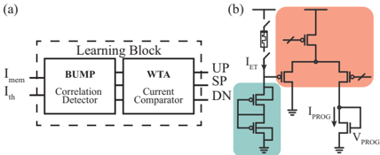
The image presents a schematic diagram of a learning block and a corresponding circuit implementation. Part (a) shows a block diagram of the learning block, while part (b) details the circuit schematic. The diagram appears to relate to neuromorphic computing or analog machine learning.
### Components/Axes
**Part (a): Learning Block**
* **Inputs:** I<sub>mem</sub>, I<sub>th</sub>
* **Internal Blocks:** BUMP, Correlation Detector, WTA (Winner-Take-All), Current Comparator
* **Outputs:** UP, SP, DN
* **Label:** "Learning Block" enclosed in a dashed rectangle.
**Part (b): Circuit Schematic**
* **Inputs:** I<sub>ET</sub>, I<sub>PROG</sub>, V<sub>PROG</sub>
* **Components:** MOSFETs (transistors), Switch
* **Color Coding:** Teal (bottom section), Peach/Salmon (top section)
* **Labels:** I<sub>ET</sub>, I<sub>PROG</sub>, V<sub>PROG</sub>, UP, SP, DN
### Detailed Analysis or Content Details
**Part (a): Learning Block**
The learning block receives two inputs: I<sub>mem</sub> and I<sub>th</sub>. These inputs feed into a "BUMP" block, which then connects to a "Correlation Detector". The output of the Correlation Detector is fed into a "Current Comparator" along with the output of the "WTA" block. The Current Comparator produces three outputs: UP, SP, and DN. The function of each block is not explicitly defined in the diagram, but the names suggest their roles in a learning process.
**Part (b): Circuit Schematic**
The circuit schematic consists of several MOSFETs arranged in a specific configuration. The top section (peach/salmon) contains a series of transistors connected to a voltage source. A switch controls the connection between I<sub>ET</sub> and the top section. The bottom section (teal) consists of a stack of transistors connected to ground. The schematic shows connections for I<sub>PROG</sub> and V<sub>PROG</sub>. The outputs UP, SP, and DN are connected to the circuit. The schematic appears to implement the functionality of the learning block described in part (a).
### Key Observations
* The diagram uses a block diagram approach for the learning block (part a) and a detailed circuit schematic for its implementation (part b).
* The color coding in part (b) may indicate different functional sections or signal paths within the circuit.
* The outputs UP, SP, and DN are consistent between the block diagram and the circuit schematic, suggesting they represent the same signals.
* The diagram does not provide specific values for currents or voltages, only labels.
### Interpretation
The diagram illustrates a potential hardware implementation of a learning block. The "BUMP" and "Correlation Detector" blocks likely perform some form of signal processing to detect patterns or correlations in the input signals. The "WTA" block selects the strongest signal, and the "Current Comparator" compares the selected signal with a threshold or reference signal. The outputs UP, SP, and DN likely control the adjustment of synaptic weights or other parameters in a learning system. The circuit schematic in part (b) provides a possible analog circuit implementation of this learning block, using MOSFETs to perform the necessary computations. The diagram suggests a neuromorphic approach to machine learning, where analog circuits are used to mimic the behavior of biological neurons and synapses. The lack of specific values suggests this is a conceptual diagram rather than a detailed design specification. The diagram is a high-level representation of a learning system, and further details would be needed to fully understand its functionality.