\n
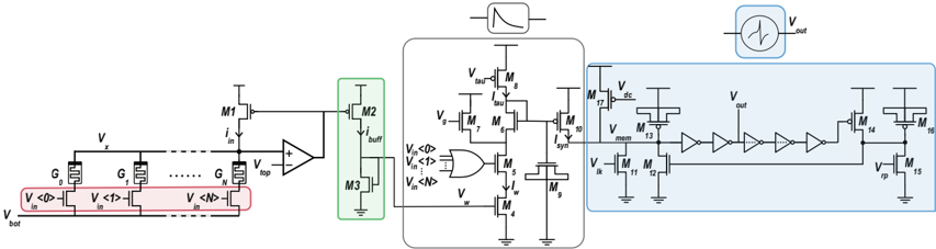
## Diagram: Operational Amplifier Circuit
### Overview
The image depicts a schematic diagram of an operational amplifier (op-amp) circuit, likely a component within a larger analog system. The diagram shows a series of transistors and other components arranged to perform amplification and signal processing. The circuit is divided into several functional blocks, including an input stage, a gain stage, and an output stage.
### Components/Axes
The diagram does not contain axes or scales in the traditional sense of a chart. Instead, it uses standard electronic schematic symbols to represent components. Key labels include:
* **V**: Represents a voltage source.
* **G**: Represents a gate terminal of a transistor.
* **V<sub>bot</sub>**: Bottom voltage.
* **V<sub>top</sub>**: Top voltage.
* **i**: Input current.
* **M1-M16**: Transistor identifiers.
* **V<sub>buff</sub>**: Buffer voltage.
* **V<sub>mem</sub>**: Memory voltage.
* **V<sub>out</sub>**: Output voltage.
* **V<sub>dc</sub>**: DC voltage.
* **V<sub>in</sub>**: Input voltage.
* **<V<sub>th</sub>>**: Threshold voltage.
* The diagram also includes symbols for an op-amp (triangle), and voltage sources (circles).
### Detailed Analysis / Content Details
The circuit can be broken down into the following sections:
1. **Input Stage (Leftmost):** This section consists of several transistors (M1-M?) connected in a differential amplifier configuration. The input voltage 'V' is applied to the gates of these transistors. The bottom voltage 'V<sub>bot</sub>' and top voltage 'V<sub>top</sub>' are also connected to the transistors. The input current 'i' is indicated.
2. **Buffer Stage (Green Box):** A single transistor (M3) is shown as a buffer, with 'V<sub>buff</sub>' as its output. The buffer receives input from the op-amp symbol.
3. **Gain Stage (Center):** This section contains a series of transistors (M4-M9) and logic gates (an OR gate). The input to this stage comes from the buffer. The threshold voltage '<V<sub>th</sub>>' is also present in this section.
4. **Output Stage (Blue Box):** This section consists of several transistors (M10-M16) and appears to be a current mirror or similar output driver configuration. The output voltage 'V<sub>out</sub>' is indicated. The DC voltage 'V<sub>dc</sub>' is also present. The output stage also contains multiple inverters (represented by triangles).
The diagram shows connections between these stages, indicating the flow of signal through the circuit. The ground symbol is present throughout the diagram.
### Key Observations
* The circuit appears to be designed for low-voltage operation, as indicated by the 'V<sub>bot</sub>' and 'V<sub>top</sub>' labels.
* The use of multiple transistors in the input stage suggests a differential amplifier configuration, which is common in op-amp designs.
* The buffer stage likely isolates the input stage from the gain stage, preventing loading effects.
* The output stage is designed to provide a low-impedance output, capable of driving a load.
### Interpretation
This diagram represents a complex analog circuit, likely a low-voltage operational amplifier. The circuit is designed to amplify a small input voltage 'V' and produce a larger output voltage 'V<sub>out</sub>'. The differential input stage provides common-mode rejection, while the buffer stage isolates the input from the gain stage. The gain stage provides the desired amplification, and the output stage drives the load. The presence of the threshold voltage '<V<sub>th</sub>>' suggests that the circuit may incorporate some form of threshold detection or switching behavior. The overall design suggests a focus on precision and low-power operation. The circuit is likely part of a larger system, such as a data converter, sensor interface, or control loop. The diagram does not provide specific numerical values for component parameters or performance characteristics, but it does provide a clear overview of the circuit's architecture and functionality.