\n
## Diagram: System Architecture Overview
### Overview
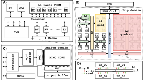
The image presents a set of four diagrams (A, B, C, and D) illustrating the architecture of a complex system, likely a specialized processor or accelerator. Diagram A shows the processing core, B depicts the memory hierarchy, C illustrates the analog domain, and D details the memory access scheme. The diagrams are interconnected through data flow and control signals.
### Components/Axes
The diagrams do not have traditional axes. Instead, they are block diagrams with labeled components and connections. Key components include:
* **Diagram A:** EV, DMA, L1 Local TCDM (B0, B1, B2, B3, B4, BN), Crossbar, IMA, RV (repeated three times), I-Cache.
* **Diagram B:** HBM, HBM Ctrl, chip domain, L1 quad, L2 quad, L3 quadrant, wrapper, CL (repeated multiple times), EF (repeated multiple times).
* **Diagram C:** Streamers, input buffer, DAC, AIMC CORE, ADC, output buffer, CTRL.
* **Diagram D:** S, L2, Q0, Q1, Q2, Q3, read, write.
### Detailed Analysis or Content Details
**Diagram A: Processing Core**
* **EV** and **DMA** feed into the **L1 Local TCDM**, which is divided into blocks B0 through BN (approximately 5 blocks shown, with BN indicating more).
* The **L1 Local TCDM** is connected to a **Crossbar** which then connects to the **IMA** and multiple **RV** units (three shown).
* The **IMA** and **RV** units connect to the **I-Cache**.
* Arrows indicate data flow between these components.
**Diagram B: Memory Hierarchy**
* **HBM** (High Bandwidth Memory) is controlled by **HBM Ctrl**.
* The **HBM** connects to the **chip domain**, which contains **L1 quad**, **L2 quad**, and **L3 quadrant**.
* The **L1 quad** and **L2 quad** are interconnected via **CL** and **EF** connections.
* The **L2 quad** connects to the **L3 quadrant** via a **wrapper**.
* The **L3 quadrant** is a large block with internal structure.
**Diagram C: Analog Domain**
* **Streamers** feed into an **input buffer**.
* The **input buffer** connects to a **DAC** (Digital-to-Analog Converter).
* The **DAC** feeds into the **AIMC CORE**.
* The **AIMC CORE** connects to an **ADC** (Analog-to-Digital Converter).
* The **ADC** outputs to an **output buffer**.
* **CTRL** signals control the flow.
**Diagram D: Memory Access Scheme**
* **S** (Start) signal initiates a memory access.
* **L2** is the primary memory level shown.
* **Q0, Q1, Q2, Q3** represent memory queues or partitions within L2.
* Arrows indicate **read** and **write** operations to the queues.
* The diagram shows a sequence of operations involving the queues.
### Key Observations
* The system employs a hierarchical memory structure (HBM, L1, L2, L3).
* There is a clear separation between the processing core (A), memory hierarchy (B), and analog domain (C).
* The memory access scheme (D) suggests a queuing mechanism for handling read and write requests.
* The use of "quad" and "quadrant" suggests a tiled or partitioned architecture.
* The diagram does not provide specific numerical values or performance metrics.
### Interpretation
The diagrams depict a highly parallel and specialized processing system. The architecture is designed for high-bandwidth data processing, likely involving analog computation (AIMC CORE) and efficient memory access. The separation of the analog domain suggests a hybrid digital-analog approach. The queuing mechanism in the memory access scheme (D) is likely implemented to manage concurrent read and write requests to the memory hierarchy, optimizing performance. The use of multiple RV units in Diagram A suggests a vector or SIMD processing capability. The overall system appears to be optimized for applications requiring high throughput and low latency, such as machine learning or signal processing. The lack of specific values makes it difficult to assess the system's performance characteristics quantitatively. The diagrams provide a high-level overview of the architecture, and further details would be needed to understand the specific implementation and capabilities of the system.