\n
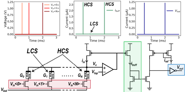
## Diagram: Circuit and Signal Waveforms
### Overview
The image presents a schematic diagram of a circuit, likely an amplifier or comparator, alongside three time-domain signal waveforms. The circuit appears to be a multi-stage amplifier with a Low-Current Switching (LCS) input and a High-Current Steering (HCS) output. The waveforms show the input voltages (V<sub>in</sub>), input current (i<sub>in</sub>), and output current (V<sub>out</sub>) over time.
### Components/Axes
The diagram consists of the following key components:
* **LCS Block:** A series of transistors (G<sub>0</sub> to G<sub>N</sub>) connected to input voltages V<sub>in</sub><0>, V<sub>in</sub><1>, and V<sub>in</sub><N>, and a bottom voltage V<sub>bot</sub>.
* **HCS Block:** Indicates the high-current steering section.
* **Operational Amplifier (Op-Amp):** A standard Op-Amp symbol with inputs V<sub>x</sub> and V<sub>top</sub>.
* **Buffer Stage:** A transistor-based buffer circuit.
* **Output Stage:** A transistor-based output stage.
* **Waveform Plots:** Three plots showing voltage and current signals over time.
* **Plot 1 (Left):** Voltage vs. Time, with axes labeled "Voltage (V)" and "Time (ms)". Includes three lines: V<sub>in</sub><0>, V<sub>in</sub><1>, and V<sub>in</sub><N>.
* **Plot 2 (Center):** Current vs. Time, with axes labeled "Current (µA)" and "Time (ms)". Includes a single line: i<sub>buff</sub>.
* **Plot 3 (Right):** Current vs. Time, with axes labeled "Current (µA)" and "Time (ms)". Includes a single line: V<sub>out</sub>.
### Detailed Analysis or Content Details
**Waveform Analysis:**
* **V<sub>in</sub><0>, V<sub>in</sub><1>, V<sub>in</sub><N> (Left Plot):** These three voltage waveforms are pulsed. Each pulse rises to approximately 1.25V and falls to 0V. The pulses are spaced approximately 1ms apart, with the first pulse starting at 0ms, the second at 1ms, and the third at 2ms. The lines are colored blue, red, and black respectively.
* **i<sub>buff</sub> (Center Plot):** This current waveform is approximately constant at 0.25 µA for the entire 3ms duration. The line is colored green.
* **V<sub>out</sub> (Right Plot):** This current waveform is pulsed, similar to the input voltages. Each pulse rises to approximately 1.25 µA and falls to 0 µA. The pulses are spaced approximately 1ms apart, with the first pulse starting at 0ms, the second at 1ms, and the third at 2ms. The line is colored blue.
**Circuit Analysis:**
* The LCS block appears to be a series of transistors acting as switches, controlled by the input voltages V<sub>in</sub><0>, V<sub>in</sub><1>, and V<sub>in</sub><N>.
* The HCS block receives input from the Op-Amp and steers current based on the amplified signal.
* The buffer stage likely provides impedance matching and isolation between the Op-Amp output and the output stage.
* The output stage appears to be a current source or current mirror, providing a controlled output current.
* The text "LCS" and "HCS" are explicitly labeled, pointing to the respective blocks.
* The input current to the Op-Amp is labeled "i<sub>in</sub>".
* The output voltage is labeled "V<sub>out</sub>".
* The input voltages to the Op-Amp are labeled "V<sub>x</sub>" and "V<sub>top</sub>".
* The bottom voltage is labeled "V<sub>bot</sub>".
### Key Observations
* The input voltages (V<sub>in</sub>) are pulsed, and the output current (V<sub>out</sub>) follows a similar pulsed pattern, suggesting a switching or amplification behavior.
* The input current (i<sub>buff</sub>) is relatively constant, indicating that the buffer stage is providing a stable current source.
* The waveforms are synchronized, with the pulses in the input voltages and output current occurring at the same time intervals.
### Interpretation
The diagram illustrates a circuit designed to switch or amplify a pulsed input signal. The LCS block likely selects one of the input voltages (V<sub>in</sub><0>, V<sub>in</sub><1>, or V<sub>in</sub><N>) based on a control signal, and the HCS block steers current based on the selected input. The Op-Amp amplifies the signal, and the buffer stage provides isolation and impedance matching. The output stage generates a pulsed output current that mirrors the input voltage pulses.
The constant input current (i<sub>buff</sub>) suggests that the buffer stage is operating in a saturation region, providing a stable current source. The synchronization between the input and output pulses indicates that the circuit is functioning as expected, with a relatively fast response time. The circuit is likely designed for low-power applications, as the input and output currents are relatively small. The use of multiple input voltages (V<sub>in</sub><0>, V<sub>in</sub><1>, V<sub>in</sub><N>) suggests that the circuit may be capable of selecting between different input signals or operating in different modes.