## Block Diagram: Digital Signal Processing Circuit
### Overview
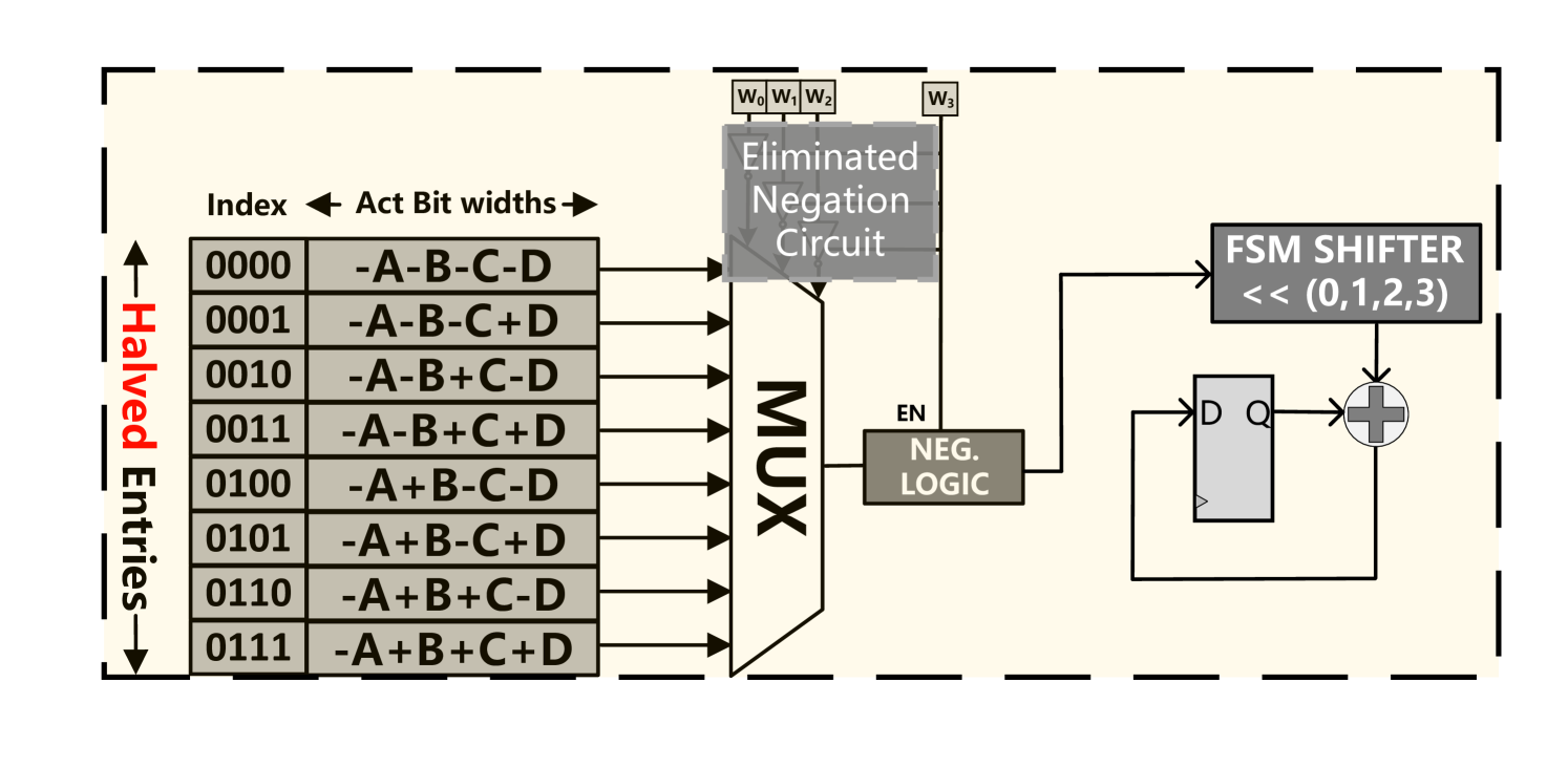
The diagram illustrates a digital signal processing circuit with a multiplexer (MUX), negation logic, an FSM shifter, and a summation component. The left side features a table of "Halved Entries" with indexed combinations of variables A, B, C, D. The right side shows signal flow through negation logic, FSM shifter, and summation.
### Components/Axes
- **Left Table**:
- **Index**: Labeled "Index" with an arrow pointing right.
- **Act Bit widths**: Labeled "Act Bit widths" with an arrow pointing right.
- **Entries**: 8 rows labeled 0000 to 0111 (binary). Each row contains a combination of A, B, C, D with signs (e.g., "-A-B-C-D", "-A-B+C+D").
- **Label**: "Halved Entries" in red, with an arrow pointing down.
- **Right Circuit**:
- **MUX**: Labeled "MUX" with inputs from the left table.
- **Negation Logic**: Labeled "NEG. LOGIC" with an "EN" (enable) signal.
- **FSM Shifter**: Labeled "FSM SHIFTER << (0,1,2,3)>>" with a control signal.
- **D Flip-Flop**: Labeled "D Q" with a "+" symbol for summation.
- **Eliminated Negation Circuit**: A gray box labeled "Eliminated Negation Circuit" above the MUX.
### Detailed Analysis
- **Left Table**:
- 8 rows represent binary indices (0000 to 0111).
- Each row combines A, B, C, D with alternating signs (e.g., "-A-B-C-D", "-A-B+C+D").
- No numerical values; entries are symbolic expressions.
- **Right Circuit**:
- **MUX**: Selects one of the 8 entries based on the index.
- **Negation Logic**: Inverts the selected signal (EN controls enable).
- **FSM Shifter**: Shifts the negated signal by 0–3 positions (control signal << (0,1,2,3)>>).
- **D Flip-Flop**: Stores the shifted value (D Q).
- **Summation**: Combines the shifted value with another input (symbolized by "+").
### Key Observations
- The "Eliminated Negation Circuit" suggests optimization to avoid redundant negation steps.
- The FSM Shifter’s control signal allows dynamic shifting, critical for timing or positional adjustments.
- The summation at the end implies the circuit aggregates processed signals.
### Interpretation
This circuit processes binary data by selecting, negating, shifting, and summing signals. The MUX and FSM Shifter enable flexible configuration, while the negation logic ensures polarity control. The "Eliminated Negation Circuit" hints at efficiency improvements, possibly reducing power consumption or latency. The summation component suggests the circuit is part of a larger system requiring combined outputs (e.g., arithmetic operations or signal synthesis).
## Additional Notes
- **Language**: All text is in English.
- **No numerical data**: The diagram focuses on symbolic logic and component relationships rather than quantitative values.
- **Flow Direction**: Signals move left-to-right, with feedback loops (e.g., D flip-flop output).