## Multi-Subplot Analysis: Electronic Device Characterization
### Overview
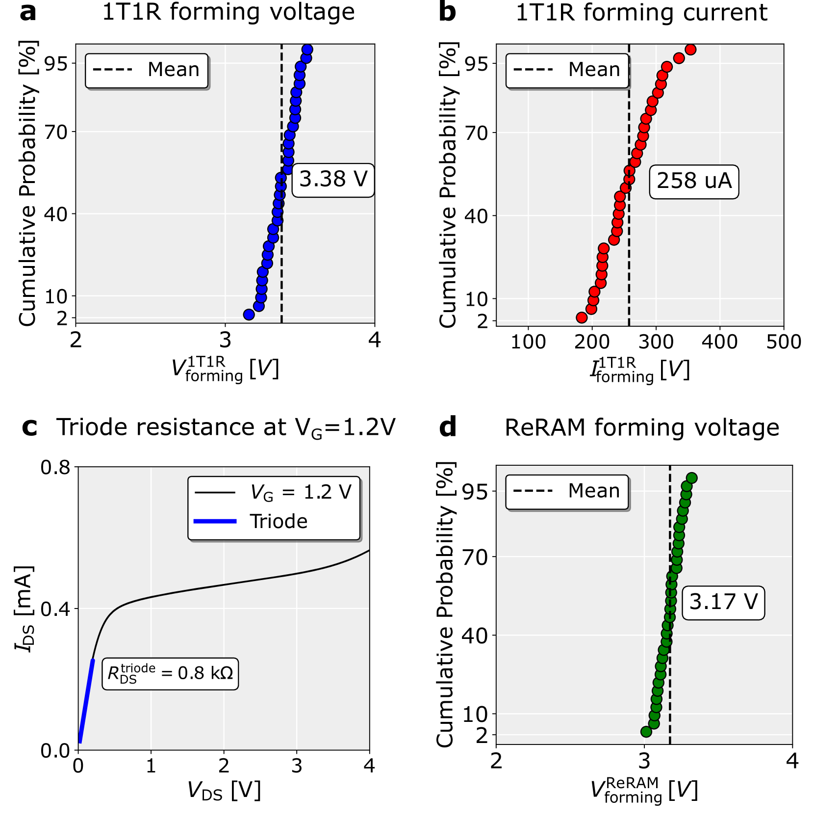
The image contains four subplots (a-d) depicting cumulative probability distributions and device characteristics for 1T1R (1 Transistor 1 Resistor) and ReRAM (Resistive Random-Access Memory) forming processes, along with triode resistance measurements. All plots use cumulative probability on the y-axis, with distinct x-axis parameters for each subplot.
### Components/Axes
**Subplot a (1T1R Forming Voltage):**
- **X-axis:** V<sub>1T1R forming</sub> [V] (Voltage range: 2-4 V)
- **Y-axis:** Cumulative Probability [%]
- **Legend:** Dashed line = Mean (3.38 V)
- **Data:** Blue circles (n=100+ data points)
- **Key Feature:** Vertical dashed line at 3.38 V
**Subplot b (1T1R Forming Current):**
- **X-axis:** I<sub>1T1R forming</sub> [μA] (Current range: 100-500 μA)
- **Y-axis:** Cumulative Probability [%]
- **Legend:** Dashed line = Mean (258 μA)
- **Data:** Red circles (n=100+ data points)
- **Key Feature:** Vertical dashed line at 258 μA
**Subplot c (Triode Resistance):**
- **X-axis:** V<sub>DS</sub> [V] (Voltage range: 0-4 V)
- **Y-axis:** I<sub>DS</sub> [mA] (Current range: 0-0.8 mA)
- **Legend:**
- Black line = V<sub>G</sub> = 1.2 V
- Blue line = Triode characteristic
- **Key Feature:** R<sub>triode DS</sub> = 0.8 kΩ annotation
**Subplot d (ReRAM Forming Voltage):**
- **X-axis:** V<sub>ReRAM forming</sub> [V] (Voltage range: 2-4 V)
- **Y-axis:** Cumulative Probability [%]
- **Legend:** Dashed line = Mean (3.17 V)
- **Data:** Green circles (n=100+ data points)
- **Key Feature:** Vertical dashed line at 3.17 V
### Detailed Analysis
**Subplot a:**
- Cumulative probability rises sharply from 20% to 95% between 3.0-3.5 V
- Mean value (3.38 V) aligns with the steepest slope region
- 95% probability achieved at ~3.8 V
**Subplot b:**
- Cumulative probability increases from 10% to 95% between 200-350 μA
- Mean value (258 μA) corresponds to the inflection point
- 95% probability reached at ~400 μA
**Subplot c:**
- Triode characteristic shows typical saturation behavior
- Linear region (V<sub>DS</sub> < 1 V) demonstrates ohmic behavior
- Saturation region (V<sub>DS</sub> > 2 V) shows near-constant current
- R<sub>triode DS</sub> = 0.8 kΩ calculated from linear region slope
**Subplot d:**
- Cumulative probability rises from 10% to 95% between 3.0-3.5 V
- Mean value (3.17 V) matches the steepest slope region
- 95% probability achieved at ~3.6 V
### Key Observations
1. All forming processes show similar sigmoidal cumulative distribution patterns
2. 1T1R forming voltage (3.38 V) and ReRAM forming voltage (3.17 V) are close but distinct
3. 1T1R forming current (258 μA) suggests current-controlled forming mechanism
4. Triode resistance (0.8 kΩ) indicates moderate channel conductance at V<sub>G</sub>=1.2 V
5. All mean values fall within the steepest slope regions of their respective distributions
### Interpretation
The data demonstrates:
- **Device Thresholds:** The mean values represent critical forming thresholds for 1T1R and ReRAM devices
- **Current-Voltage Relationship:** Subplot c reveals that 1T1R forming occurs at moderate V<sub>DS</sub> where triode resistance is established
- **Probability Distributions:** The similar shapes across subplots a, b, and d suggest comparable forming mechanisms despite different physical parameters
- **Process Control:** The narrow probability distributions (95% within ~0.5 V/μA) indicate precise forming process control
- **Material Properties:** The triode resistance measurement provides insight into channel quality and interface states
The close proximity of 1T1R forming voltage (3.38 V) and ReRAM forming voltage (3.17 V) suggests potential for co-integration of these technologies, while the distinct current threshold (258 μA) highlights the importance of current control in 1T1R forming processes.