TECHNICAL ASSET FINGERPRINT
96a99239a3f48246e9c6ef69
Click to view fullscreen
Press ESC or click to close
FOUND IN PAPERS
EXPERT: healer-alpha-free VERSION 1
RUNTIME: free/openrouter/healer-alpha
INTEL_VERIFIED
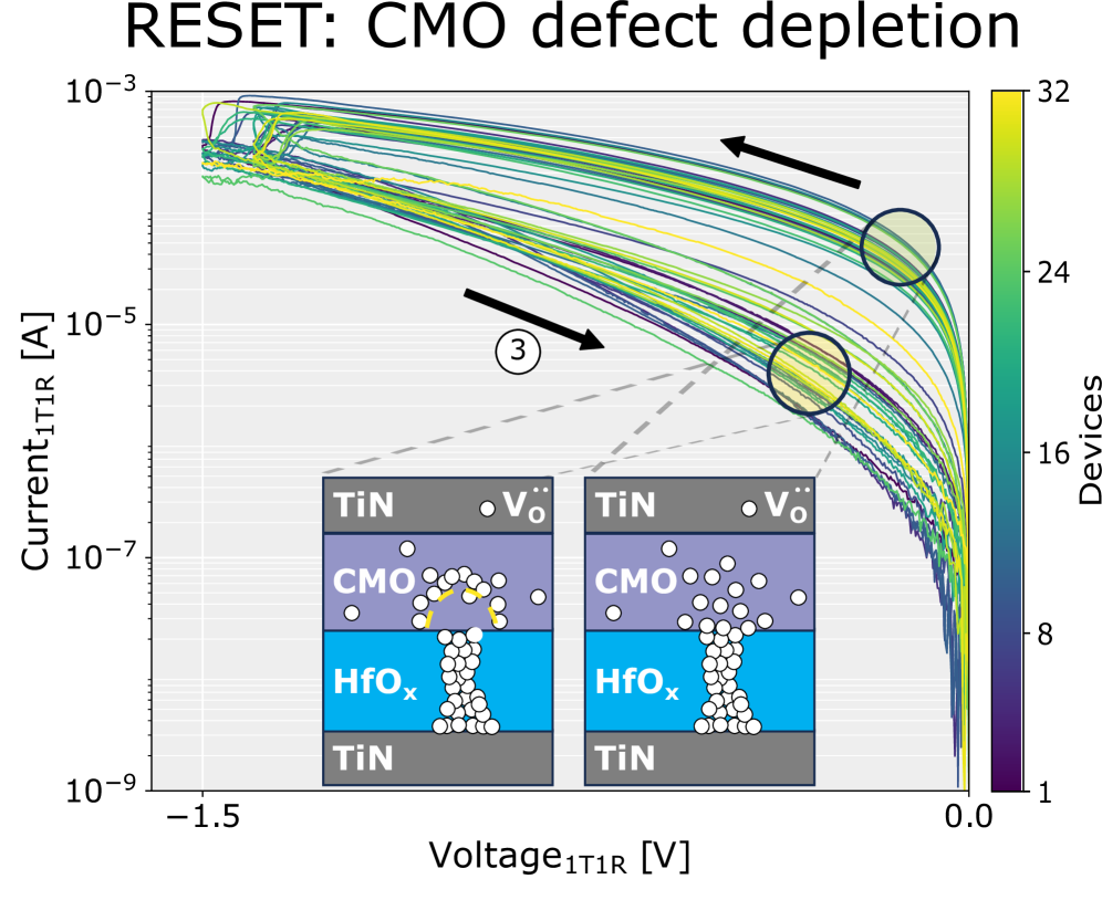
## Chart: RESET Characteristics of CMO-Based Resistive Switching Devices
### Overview
This image is a scientific plot titled "RESET: CMO defect depletion." It displays the current-voltage (I-V) characteristics for multiple devices during a RESET operation, which transitions a resistive switching memory cell from a low-resistance state (LRS) to a high-resistance state (HRS). The plot includes a main chart and an inset schematic diagram illustrating the proposed physical mechanism.
### Components/Axes
1. **Main Chart:**
* **X-axis:** `Voltage₁T₁R [V]`. The scale is linear, ranging from -1.5 V on the left to 0.0 V on the right.
* **Y-axis:** `Current₁T₁R [A]`. The scale is logarithmic, ranging from 10⁻⁹ A at the bottom to 10⁻³ A at the top.
* **Data Series:** Multiple colored lines, each representing the I-V curve of a single device. The lines are colored according to a gradient scale.
* **Color Bar/Legend:** Located on the far right. It is labeled "Devices" and maps the line color to a device number, ranging from 1 (dark purple) to 32 (bright yellow). The gradient progresses from purple (low device number) through blue, green, to yellow (high device number).
* **Annotations:**
* A black arrow points from the top-right towards the center-left, indicating the general direction of the voltage sweep (from 0V to negative voltage).
* A circled number "3" with a black arrow points to a specific region of the curves.
* Two black circles highlight specific regions on the bundle of curves.
* Dashed grey lines connect the inset diagram to the highlighted regions on the main plot.
2. **Inset Schematic Diagram (Bottom Center):**
* This diagram shows a cross-section of the device stack in two states, illustrating the proposed "defect depletion" mechanism.
* **Layers (from top to bottom):**
* `TiN` (Titanium Nitride, top electrode)
* `CMO` (Complex Metal Oxide, switching layer)
* `HfOₓ` (Hafnium Oxide, another oxide layer)
* `TiN` (Titanium Nitride, bottom electrode)
* **Key Symbols:**
* White circles: Represent oxygen vacancies (Vö), labeled as `Vö` with a dot above the 'o'.
* Yellow arrows within the CMO layer: Indicate the movement or depletion of oxygen vacancies.
* **Two States:**
* **Left State:** Shows a dense filament of oxygen vacancies (white circles) connecting through the HfOₓ layer and extending into the CMO layer. This represents the Low-Resistance State (LRS).
* **Right State:** Shows the filament in the HfOₓ layer remains, but the vacancies in the CMO layer have been depleted or dispersed away from the filament tip. This represents the High-Resistance State (HRS) after the RESET process.
### Detailed Analysis
* **Data Trend:** All I-V curves show a similar trend. As the voltage sweeps from 0.0 V to -1.5 V (leftward), the current initially remains relatively high (between ~10⁻⁴ A and 10⁻³ A) and then undergoes a steep, non-linear drop (by several orders of magnitude) as the voltage becomes more negative. This drop signifies the RESET transition from LRS to HRS.
* **Variability:** There is significant device-to-device variability. The voltage at which the sharp current drop occurs (the RESET voltage) varies across the 32 devices. The curves colored yellow (higher device numbers) generally appear to undergo the transition at slightly less negative voltages (closer to -1.0 V) compared to some purple/blue curves (which transition closer to -1.2 V or beyond). The final HRS current at -1.5 V also varies, spanning from below 10⁻⁸ A to nearly 10⁻⁷ A.
* **Highlighted Regions:**
* The upper circled region (connected to the right inset diagram) encompasses the "knee" of the curves where the current begins its steep descent. This corresponds to the onset of the RESET process.
* The lower circled region (connected to the left inset diagram) is in the midst of the steep current drop, representing the active RESET transition where the conductive filament is being disrupted.
### Key Observations
1. **Universal Behavior:** All 32 devices exhibit the fundamental RESET switching characteristic—a sharp decrease in current under negative voltage bias.
2. **Stochastic Nature:** The exact RESET voltage and the slope of the transition are not identical across devices, highlighting the stochastic (random) nature of filament rupture in resistive switching memory.
3. **Correlation with Mechanism:** The inset diagram provides a physical model to explain the electrical data. The RESET process is attributed to the depletion of oxygen vacancies (defects) from the conductive filament specifically within the CMO layer, breaking the conductive path.
4. **Logarithmic Scale:** The use of a logarithmic Y-axis is essential to visualize the current change over six orders of magnitude (from mA to nA range).
### Interpretation
This chart demonstrates the electrical signature and a proposed physical mechanism for the RESET operation in a TiN/CMO/HfOₓ/TiN memory device stack.
* **What the data suggests:** The steep, sigmoidal drop in current under negative bias is the classic electrical indicator of a resistive switching RESET event. The variability in the curves suggests that while the underlying mechanism is consistent, the precise atomic-scale configuration of the filament and its rupture process varies from cycle to cycle and device to device.
* **How elements relate:** The main plot provides the macroscopic electrical evidence (I-V curves), while the inset offers a microscopic, physical explanation. The dashed lines explicitly link the electrical behavior (the "knee" and the drop) to the proposed structural change in the device (depletion of vacancies in the CMO layer).
* **Notable patterns/anomalies:** The most notable pattern is the tight bundling of curves followed by their divergence during the transition, which visually captures the interplay between a deterministic switching mechanism and its stochastic execution. There are no major outliers; all devices follow the same general path, confirming the robustness of the switching phenomenon in this material system.
* **Underlying Significance:** This data is critical for understanding and optimizing resistive RAM (RRAM) devices. The RESET operation is fundamental for writing data (e.g., a "0"). The observed variability is a key challenge for large-scale memory integration, as it affects device reliability and the design of read/write circuitry. The proposed "defect depletion" model in the CMO layer offers a specific target for material engineering to improve switching uniformity and control.
DECODING INTELLIGENCE...