## Line Chart: RESET: CMO Defect Depletion
### Overview
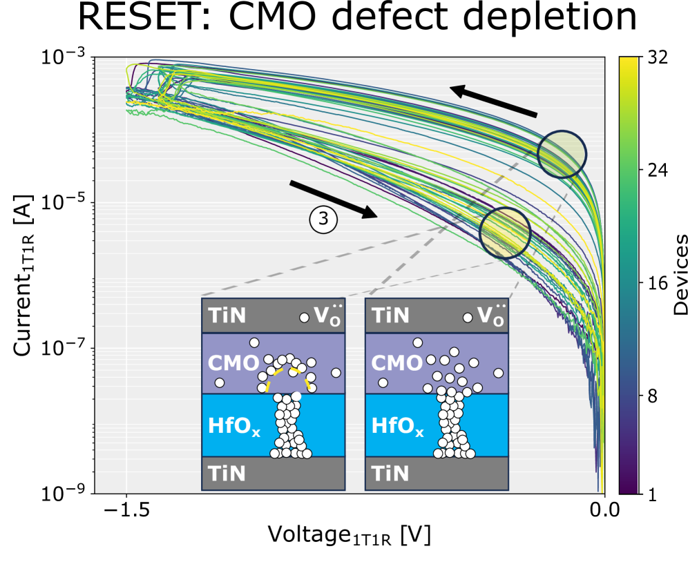
The image depicts a logarithmic line chart illustrating the relationship between current (Current₁T1R) and voltage (Voltage₁T1R) during conductive metal oxide (CMO) defect depletion in a TiN/HfOₓ/TiN structure. Multiple colored lines represent different device configurations, with a color gradient indicating the number of devices (1–32). Two insets below the main graph show schematic diagrams of the material layers before and after defect depletion.
---
### Components/Axes
- **Y-Axis (Left)**:
- Label: `Current₁T1R [A]`
- Scale: Logarithmic (10⁻⁹ to 10⁻³ A)
- Position: Left side of the chart
- **X-Axis (Bottom)**:
- Label: `Voltage₁T1R [V]`
- Scale: Linear (-1.5 V to 0.0 V)
- Position: Bottom of the chart
- **Color Bar (Right)**:
- Label: `Devices`
- Scale: 1 (purple) to 32 (yellow)
- Position: Right side of the chart
- **Insets (Bottom Center)**:
- Two diagrams labeled `TiN`, `CMO`, and `HfOₓ` with white dots representing defects.
- Left inset: CMO defects clustered in HfOₓ layer.
- Right inset: CMO defects dispersed in TiN layer.
---
### Detailed Analysis
1. **Lines**:
- **Trend**: All lines slope downward from the top-left (high current, low voltage) to the bottom-right (low current, high voltage), indicating current reduction as voltage increases.
- **Color Gradient**:
- Purple lines (1 device): Minimal current drop, suggesting fewer defects.
- Yellow lines (32 devices): Steeper current drop, indicating higher initial defect density.
- **Notable Features**:
- Lines converge near the origin (0 V, 10⁻⁹ A), suggesting complete defect depletion at higher voltages.
- Two circular annotations (① and ②) highlight specific voltage/current points.
2. **Insets**:
- **Left Inset**:
- CMO defects (white dots) concentrated in the HfOₓ layer between TiN electrodes.
- Voltage polarity (`V_O`) indicated by arrows.
- **Right Inset**:
- CMO defects dispersed into the TiN layer, representing post-depletion state.
---
### Key Observations
- **Defect Depletion Correlation**: Devices with higher initial defect density (yellow lines) exhibit steeper current-voltage curves, confirming that defect depletion reduces conductivity.
- **Voltage Threshold**: All lines plateau near 0 V, implying a critical voltage range for effective defect migration.
- **Material Layer Dynamics**: Insets suggest HfOₓ acts as a defect reservoir, while TiN facilitates defect migration.
---
### Interpretation
The chart demonstrates that applying voltage (`V_O`) drives CMO defects from the HfOₓ layer into the TiN electrodes, reducing interfacial conductivity. The color-coded lines quantify this effect across 32 devices, showing that higher defect densities (yellow) require greater voltage to achieve depletion. The insets provide a physical model: HfOₓ initially traps defects, but voltage-induced electric fields redistribute them into TiN, altering the device’s resistive state. This aligns with resistive random-access memory (ReRAM) mechanisms, where defect migration modulates conductivity.
**Critical Insight**: The convergence of lines at low current values suggests a universal depletion threshold, independent of initial defect density. This could inform optimization of ReRAM devices for consistent performance.