\n
## Diagram: Data Synchronization Flow
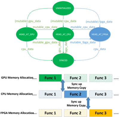
### Overview
The image depicts a diagram illustrating the data synchronization process between a GPU, CPU, and FPGA. The diagram is divided into two main sections: a state transition diagram at the top and a functional allocation diagram at the bottom. The state transition diagram shows the progression of data from an "UNINITIALIZED" state to a "SYNCED" state, involving intermediate states representing data residing on the GPU, CPU, and FPGA. The functional allocation diagram shows how functions are allocated to each memory space and the data transfer between them.
### Components/Axes
The diagram consists of the following components:
* **States:** UNINITIALIZED, HEAD\_AT\_GPU, HEAD\_AT\_CPU, HEAD\_AT\_FPGA, SYNCED.
* **Data Labels:** mutable gpu\_data, mutable cpu\_data, mutable fpga\_data, cpu\_data, gpu\_data, fpga\_data.
* **Memory Allocations:** GPU Memory Allocation, CPU Memory Allocation, FPGA Memory Allocation.
* **Functions:** Func 1, Func 2, Func 3.
* **Data Transfer Operations:** Sync up Memory Copy.
### Detailed Analysis or Content Details
**State Transition Diagram (Top Section):**
* **UNINITIALIZED (Green):** The initial state. Arrows originate from this state, labeled "mutable gpu\_data", "mutable cpu\_data", and "mutable fpga\_data", pointing to the "HEAD\_AT\_GPU", "HEAD\_AT\_CPU", and "HEAD\_AT\_FPGA" states respectively.
* **HEAD\_AT\_GPU (Light Green):** Receives data from "UNINITIALIZED" via "mutable gpu\_data". An arrow labeled "mutable\_cpu\_data" points from this state to "HEAD\_AT\_CPU". An arrow labeled "cpu\_data" points back to the "SYNCED" state.
* **HEAD\_AT\_CPU (Light Blue):** Receives data from "HEAD\_AT\_GPU" via "mutable\_cpu\_data". An arrow labeled "mutable\_fpga\_data" points from this state to "HEAD\_AT\_FPGA". An arrow labeled "gpu\_data" points back to the "SYNCED" state.
* **HEAD\_AT\_FPGA (Light Yellow):** Receives data from "HEAD\_AT\_CPU" via "mutable\_fpga\_data". An arrow labeled "cpu\_data" points back to the "SYNCED" state.
* **SYNCED (Green):** Receives data from "HEAD\_AT\_GPU", "HEAD\_AT\_CPU", and "HEAD\_AT\_FPGA".
**Functional Allocation Diagram (Bottom Section):**
* **GPU Memory Allocation:**
* Func 1 (Dark Green): Positioned on the left.
* Func 2 (Dark Green): Positioned in the center, with a bidirectional arrow labeled "Sync up Memory Copy" pointing to Func 2 in the CPU Memory Allocation row.
* Func 3 (Dark Green): Positioned on the right.
* **CPU Memory Allocation:**
* Func 1 (Light Blue): Positioned on the left.
* Func 2 (Dark Blue): Positioned in the center, with a bidirectional arrow labeled "Sync up Memory Copy" pointing to Func 2 in the FPGA Memory Allocation row.
* Func 3 (Light Blue): Positioned on the right.
* **FPGA Memory Allocation:**
* Func 1 (Light Yellow): Positioned on the left.
* Func 2 (Light Yellow): Positioned in the center.
* Func 3 (Dark Yellow): Positioned on the right.
### Key Observations
* The state transition diagram shows a three-way synchronization process involving the GPU, CPU, and FPGA.
* The functional allocation diagram indicates that Func 2 is responsible for synchronizing data between the GPU and CPU, and between the CPU and FPGA.
* The "Sync up Memory Copy" operation suggests a data transfer mechanism between the different memory spaces.
* Func 1 and Func 3 appear to be independent operations within each memory space.
### Interpretation
The diagram illustrates a data synchronization pipeline where data initially resides in an uninitialized state and is then distributed to the GPU, CPU, and FPGA. The "HEAD\_AT\_" states likely represent the location where the data's processing head is currently located. The "SYNCED" state signifies that all three components have access to the data.
The functional allocation diagram highlights the role of Func 2 in facilitating data transfer between the different memory spaces. The bidirectional arrows labeled "Sync up Memory Copy" suggest that data is copied back and forth between the GPU, CPU, and FPGA, potentially for consistency or redundancy.
The diagram suggests a system where data processing is distributed across the GPU, CPU, and FPGA, with Func 2 acting as a central synchronization point. The allocation of Func 1 and Func 3 to each memory space indicates that these functions are performed locally on each component. The diagram does not provide any information about the nature of the functions or the data being synchronized, but it clearly outlines the flow of data and the roles of the different components in the synchronization process. The use of different colors for the functions in each memory allocation row may indicate different implementations or optimizations for each platform.