# Technical Data Extraction: Spatial Current Distribution Plots
This document provides a comprehensive extraction of the data and visual information contained in the provided image, which consists of two side-by-side heatmaps representing physical simulations.
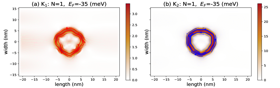
## 1. General Metadata
* **Image Type:** Scientific Heatmap / Contour Plot with Vector Overlays.
* **Language:** English.
* **Primary Units:** Nanometers (nm) for spatial dimensions; millielectronvolts (meV) for energy.
* **Common Axis Parameters:**
* **X-axis (Length):** Range from -20 to 20 nm. Markers at intervals of 5 units (-20, -15, -10, -5, 0, 5, 10, 15, 20).
* **Y-axis (Width):** Range from -15 to 15 nm. Markers at intervals of 5 units (-15, -10, -5, 0, 5, 10, 15).
---
## 2. Component Isolation: Panel (a)
### Header Information
* **Title:** (a) $K_1$: N=1, $E_F$=-35 (meV)
* **Interpretation:** This panel represents the $K_1$ valley/state for a single particle (N=1) at a Fermi energy of -35 meV.
### Main Chart Data
* **Spatial Distribution:** A central ring-like structure is located between -7 nm and +7 nm on the x-axis and -7 nm and +7 nm on the y-axis.
* **Visual Trend:** The intensity is concentrated in a hexagonal/circular ring. Inside the ring, there are three distinct "lobes" or sub-peaks of higher intensity arranged in a triangular pattern around the center (0,0).
* **Vector Overlay:** Red streamlines with arrows indicate the flow of current. The flow is **clockwise** around the central structure.
* **Intensity Scale (Colorbar):**
* **Location:** Right side of panel (a).
* **Range:** 0.0 to 3.0+ (top marker is 3.0, but the gradient extends slightly higher).
* **Color Gradient:** White (0.0) $\rightarrow$ Light Orange $\rightarrow$ Dark Red/Brown (~3.0).
---
## 3. Component Isolation: Panel (b)
### Header Information
* **Title:** (b) $K_2$: N=1, $E_F$=-35 (meV)
* **Interpretation:** This panel represents the $K_2$ valley/state for a single particle (N=1) at a Fermi energy of -35 meV.
### Main Chart Data
* **Spatial Distribution:** Similar to panel (a), a central ring-like structure is centered at (0,0), spanning roughly -7 nm to +7 nm in both dimensions.
* **Visual Trend:** The intensity distribution is more uniform along the ring compared to panel (a), forming a clearer hexagonal shape with a hollow center.
* **Vector Overlay:** Blue streamlines with arrows indicate the flow of current. The flow is **counter-clockwise** around the central structure.
* **Intensity Scale (Colorbar):**
* **Location:** Right side of panel (b).
* **Range:** 0 to 25.
* **Color Gradient:** White (0) $\rightarrow$ Orange $\rightarrow$ Dark Red (25).
* **Note:** The magnitude of the values in panel (b) is significantly higher (up to 25) compared to panel (a) (up to 3).
---
## 4. Comparative Analysis & Summary
| Feature | Panel (a) $K_1$ | Panel (b) $K_2$ |
| :--- | :--- | :--- |
| **Peak Magnitude** | ~3.0 - 3.5 | ~25.0 |
| **Current Direction** | Clockwise (Red arrows) | Counter-clockwise (Blue arrows) |
| **Internal Structure** | Three-lobed internal peaks | Uniform hexagonal ring |
| **Spatial Extent** | ~14 nm diameter | ~14 nm diameter |
**Technical Conclusion:**
The images depict the current density and flow for two different states ($K_1$ and $K_2$). While the spatial footprint of the current is similar in size and location for both, the $K_2$ state exhibits a current magnitude approximately 8 times stronger than the $K_1$ state. Crucially, the states exhibit opposite chirality (direction of flow), a characteristic often associated with valley-polarized transport in 2D materials like graphene or TMDs.