\n
## Diagram: Neural Network Input Stage with LBM
### Overview
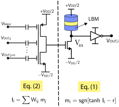
The image depicts a schematic diagram of an input stage for a neural network, incorporating a Local Binary Memory (LBM). The diagram shows a series of input voltages (Vbias,i, Vout,j, Vout,j+n) connected to a transistor stack, which then feeds into an LBM element. The output of the LBM is then processed by an inverter to produce the final output voltage (Vout,i). Two equations are provided below the diagram.
### Components/Axes
The diagram consists of the following components:
* **Input Voltages:** Vbias,i, Vout,j, Vout,j+n.
* **Transistor Stack:** A series of transistors connected between +VDD/2 and -VDD/2.
* **LBM (Local Binary Memory):** Represented as a cylindrical capacitor with blue and yellow bands.
* **Inverter:** A standard CMOS inverter.
* **Voltage Sources:** +VDD/2 and -VDD/2.
* **Intermediate Voltage:** Vm.
* **Equations:** Eq. (1) and Eq. (2).
### Content Details
The diagram can be divided into three main sections: the input stage, the LBM, and the output stage.
**Input Stage:**
* Multiple input voltages are present: Vbias,i, Vout,j, and Vout,j+n. The "..." indicates that there are potentially more Vout inputs.
* These inputs are connected to the gates of transistors in the stack.
* The transistor stack is connected to +VDD/2 at the top and -VDD/2 at the bottom.
**LBM:**
* The output of the transistor stack is connected to one terminal of the LBM.
* The other terminal of the LBM is connected to a voltage source Vm.
* The LBM is connected to an inverter.
**Output Stage:**
* The output of the inverter is labeled Vout,i.
**Equations:**
* **Eq. (1):** m<sub>i</sub> = sgn[tanh I<sub>i</sub> – r]
* **Eq. (2):** I<sub>i</sub> = Σ w<sub>ij</sub> m<sub>j</sub>
Where:
* m<sub>i</sub> and m<sub>j</sub> are likely binary memory states.
* I<sub>i</sub> is a current.
* w<sub>ij</sub> are weights.
* r is a threshold.
* sgn is the sign function.
### Key Observations
* The diagram illustrates a neural network architecture that utilizes a local binary memory element.
* The LBM appears to be a key component in the network's functionality.
* The equations suggest a weighted sum of binary memory states is used to calculate a current, which is then used to determine the memory state.
* The dashed vertical line separates the input stage from the LBM and output stage.
### Interpretation
The diagram represents a simplified model of a neural network input stage. The transistor stack acts as a current source or sink, controlled by the input voltages. The LBM stores binary information, and the equations suggest that the network learns by adjusting the weights (w<sub>ij</sub>) to modify the current flow and, consequently, the memory states. The inverter provides a logic function to produce the final output. The use of an LBM suggests a focus on low-power or analog computation. The equations provide a mathematical description of the LBM's operation, indicating a threshold-based activation function (tanh and sgn). The overall architecture suggests a system capable of pattern recognition or classification based on the weighted sum of inputs and the stored binary information. The diagram is a conceptual representation and does not specify the exact implementation details of the transistors or the LBM.