TECHNICAL ASSET FINGERPRINT
b8713c039af5992d18d27b52
Click to view fullscreen
Press ESC or click to close
FOUND IN PAPERS
EXPERT: healer-alpha-free VERSION 1
RUNTIME: free/openrouter/healer-alpha
INTEL_VERIFIED
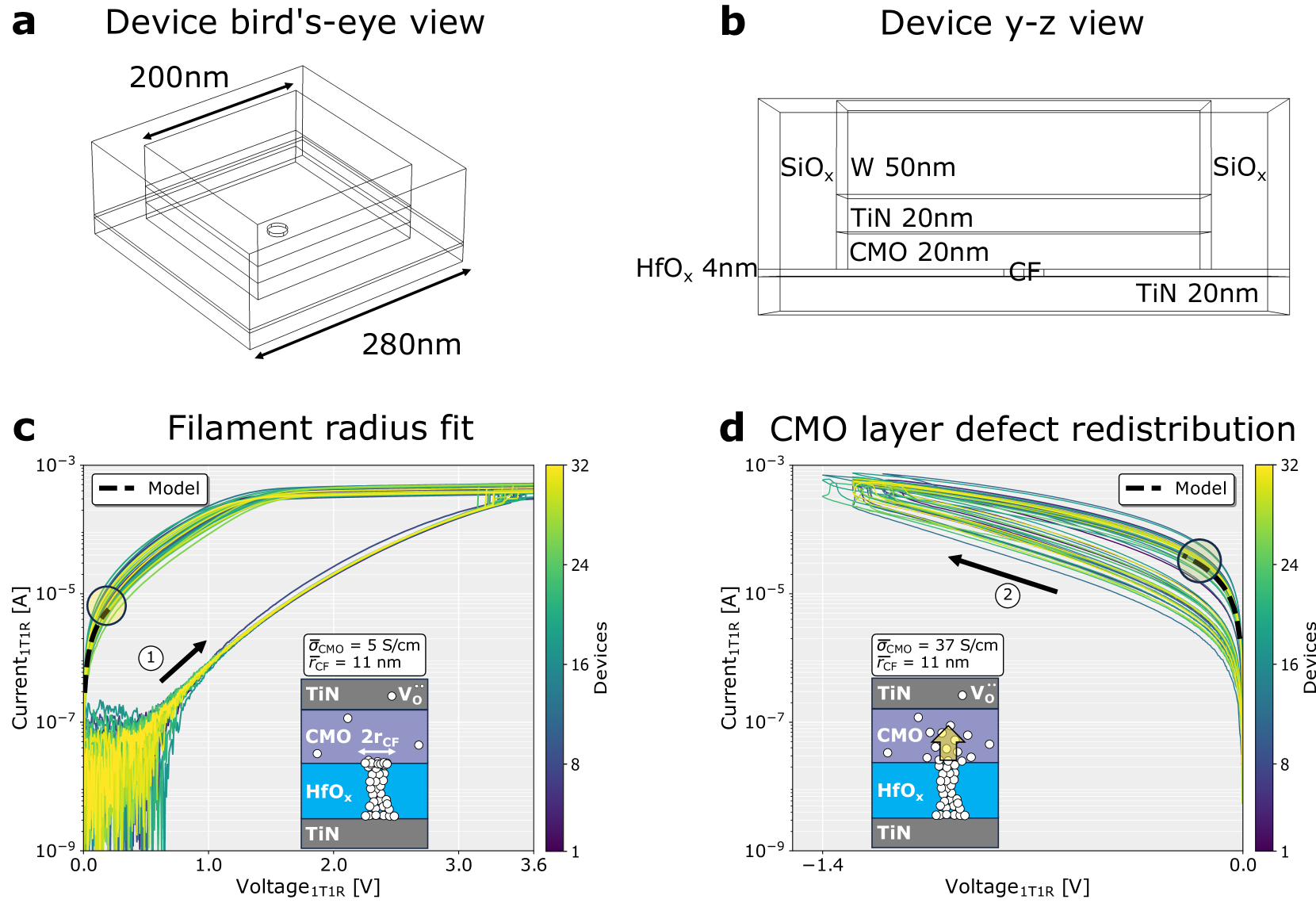
## [Technical Diagram & Data Charts]: Memristor Device Structure and Electrical Characteristics
### Overview
The image is a four-panel composite figure (labeled a, b, c, d) detailing the physical structure and electrical performance of a resistive switching memory device (memristor). Panels a and b are schematic diagrams of the device geometry and material stack. Panels c and d are data charts showing current-voltage (I-V) characteristics, with fitted models and insets illustrating the proposed physical mechanism.
### Components/Axes
**Panel a: Device bird's-eye view**
* **Type:** 3D wireframe schematic.
* **Content:** Shows the top-down perspective of a rectangular device structure.
* **Labels/Dimensions:**
* Top edge: "200nm" (with a double-headed arrow indicating width).
* Bottom edge: "280nm" (with a double-headed arrow indicating length).
* A small circular feature is visible in the center of the top surface.
**Panel b: Device y-z view**
* **Type:** 2D cross-sectional schematic.
* **Content:** Shows the vertical material stack of the device.
* **Labels/Materials & Thicknesses (from top to bottom):**
* Top and side encapsulation: "SiOₓ"
* Top electrode: "W 50nm" (Tungsten, 50 nanometers thick)
* Barrier/adhesion layer: "TiN 20nm" (Titanium Nitride, 20 nm)
* Switching layer: "CMO 20nm" (20 nm)
* Interface layer: "HfOₓ 4nm" (Hafnium Oxide, 4 nm)
* Bottom electrode: "TiN 20nm" (20 nm)
* A vertical line labeled "CF" (likely Conductive Filament) is drawn through the HfOₓ and CMO layers.
**Panel c: Filament radius fit**
* **Type:** Semi-logarithmic line chart.
* **Title:** "Filament radius fit"
* **Y-axis:** Label: "Current₁T₁R [A]" (Current for a 1-Transistor 1-Resistor cell, in Amperes). Scale: Logarithmic, from 10⁻⁹ to 10⁻³.
* **X-axis:** Label: "Voltage₁T₁R [V]" (Voltage, in Volts). Scale: Linear, from 0.0 to 3.6.
* **Legend:** A black dashed line labeled "Model".
* **Data Series:** Multiple colored lines (blue to yellow gradient) representing different devices. A black dashed "Model" line follows the upper envelope of the data.
* **Color Bar (Right):** Labeled "Devices". Scale: Linear, from 1 (dark blue) to 32 (yellow). Indicates the number of devices exhibiting a given I-V curve.
* **Annotations:**
* A circled region at low voltage (~0.1V, 10⁻⁷ A) with an arrow labeled "①" pointing to the right, indicating the SET process (transition to low resistance).
* An inset schematic in the bottom-right corner showing the material stack (TiN/CMO/HfOₓ/TiN) with a conductive filament (white circles) and oxygen vacancies (Vₒ̈). Text inside: "σ̄_CMO = 5 S/cm" and "r̄_CF = 11 nm".
**Panel d: CMO layer defect redistribution**
* **Type:** Semi-logarithmic line chart.
* **Title:** "CMO layer defect redistribution"
* **Y-axis:** Label: "Current₁T₁R [A]". Scale: Logarithmic, from 10⁻⁹ to 10⁻³.
* **X-axis:** Label: "Voltage₁T₁R [V]". Scale: Linear, from -1.4 to 0.0.
* **Legend:** A black dashed line labeled "Model".
* **Data Series:** Multiple colored lines (blue to yellow gradient) representing different devices during a RESET process (transition to high resistance). A black dashed "Model" line follows the lower envelope of the data.
* **Color Bar (Right):** Identical to panel c, labeled "Devices" from 1 to 32.
* **Annotations:**
* A circled region at higher negative voltage (~-0.8V, 10⁻⁵ A) with an arrow labeled "②" pointing to the left, indicating the RESET process.
* An inset schematic in the bottom-left corner showing the material stack. An upward yellow arrow indicates oxygen vacancy migration away from the filament. Text inside: "σ̄_CMO = 37 S/cm" and "r̄_CF = 11 nm".
### Detailed Analysis
**Panel c (Filament radius fit - SET Process):**
* **Trend:** The data lines show a sharp, non-linear increase in current (over 4 orders of magnitude) as voltage increases from ~0.0V to ~0.5V, characteristic of a resistive switching "SET" operation. Above ~1.0V, the current saturates near 10⁻⁴ A.
* **Data Points (Approximate from Model Line):**
* At 0.0V: Current ~10⁻⁸ A.
* At 0.2V: Current ~10⁻⁶ A (beginning of steep rise).
* At 0.5V: Current ~10⁻⁴ A (reaching high-conductance state).
* At 3.6V: Current ~5x10⁻⁴ A.
* **Model Parameters (Inset):** The fitted model assumes an average CMO conductivity (σ̄_CMO) of 5 S/cm and an average conductive filament radius (r̄_CF) of 11 nm.
**Panel d (CMO layer defect redistribution - RESET Process):**
* **Trend:** The data lines show a gradual decrease in current as the magnitude of negative voltage increases from 0.0V to ~-1.0V. This is the "RESET" process, transitioning the device back to a high-resistance state.
* **Data Points (Approximate from Model Line):**
* At 0.0V: Current ~10⁻⁴ A (starting from the low-resistance state).
* At -0.5V: Current ~10⁻⁵ A.
* At -1.0V: Current ~10⁻⁶ A.
* At -1.4V: Current ~10⁻⁷ A.
* **Model Parameters (Inset):** The fitted model for the RESET process assumes a higher average CMO conductivity (σ̄_CMO) of 37 S/cm, while the filament radius (r̄_CF) remains 11 nm.
### Key Observations
1. **Device Structure:** The device is a TiN/CMO/HfOₓ/TiN stack, with the CMO (20nm) and HfOₓ (4nm) layers forming the active switching medium.
2. **Switching Asymmetry:** The SET process (panel c) is abrupt and occurs at low positive voltage (<0.5V). The RESET process (panel d) is more gradual and requires higher magnitude negative voltage (>-1.0V for significant current drop).
3. **Device Variability:** The spread of colored lines in both charts indicates variability in the electrical characteristics across the 32 measured devices. The yellow lines (representing a higher count of devices) cluster around the model lines.
4. **Model Fit:** The black dashed "Model" lines provide a good fit to the envelope of the experimental data in both switching directions.
5. **Proposed Mechanism:** The insets and titles suggest the switching mechanism involves the formation/dissolution of a conductive filament (CF) with a radius of ~11 nm, coupled with the redistribution of defects (likely oxygen vacancies, Vₒ̈) within the CMO layer, altering its conductivity.
### Interpretation
This figure presents a comprehensive characterization of a bilayer (CMO/HfOₓ) memristive device. The data demonstrates reliable bipolar resistive switching, where a positive voltage forms a conductive filament (SET, panel c), and a negative voltage disrupts it (RESET, panel d).
The key scientific insight is the correlation between the electrical behavior and a physical model. The model successfully fits the data by accounting for two parameters: the filament radius and, crucially, the **conductivity of the CMO layer**. The significant increase in the fitted CMO conductivity (from 5 S/cm during SET to 37 S/cm during RESET) strongly suggests that the RESET process is not merely filament rupture, but involves a **redistribution of defects (oxygen vacancies) away from the filament region into the surrounding CMO matrix**, thereby increasing its overall conductivity and reducing the current through the device. This provides a more nuanced understanding of the switching mechanism beyond simple filament geometry changes.
The variability shown across 32 devices highlights a common challenge in memristor technology, but the consistent fit of the model suggests the underlying physical mechanism is robust. The precise dimensions (200nm x 280nm area, specific layer thicknesses) are critical for reproducing this behavior and scaling the technology.
DECODING INTELLIGENCE...