## Technical Diagram Analysis: Device Structure and Electrical Characteristics
### Overview
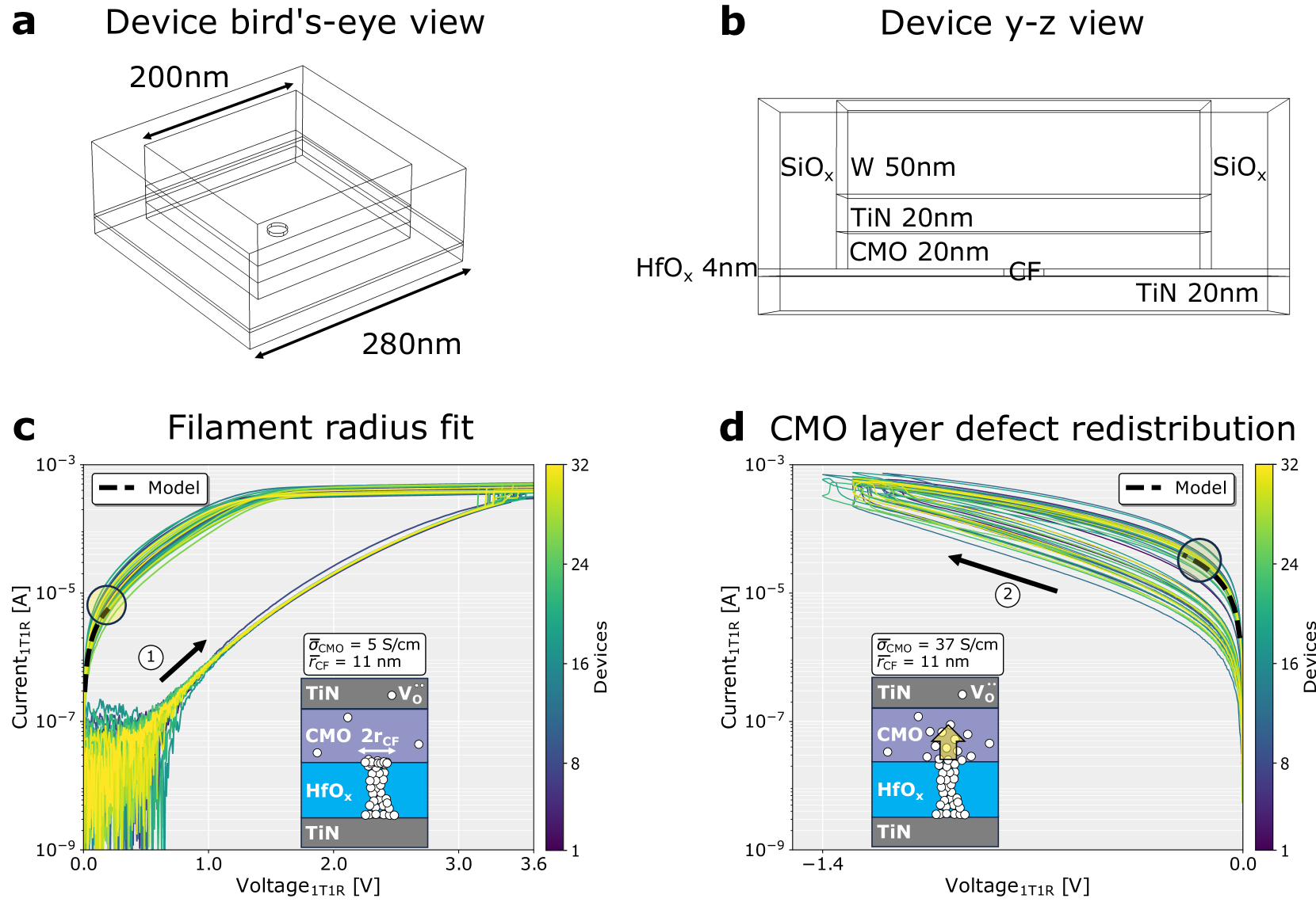
The image presents a multi-part technical analysis of a nanoscale electronic device, combining structural diagrams (a-b) with electrical characterization graphs (c-d). The device appears to be a thin-film transistor or memory element with layered dielectric and conductive components.
### Components/Axes
**a) Device Bird's-Eye View**
- Dimensions: 200nm x 280nm
- Structure: Square geometry with central void
- Key components: Not explicitly labeled in this view
**b) Device y-z Cross-Section**
- Layer stack (top to bottom):
1. SiO₂ (50nm)
2. TiN (20nm)
3. CMO (20nm)
4. HfOₓ (4nm)
5. CF (conductive filament)
6. TiN (20nm)
7. SiO₂ (50nm)
- Interface labels: CF (conductive filament) at bottom
**c) Filament Radius Fit Graph**
- Axes:
- X: Voltage₁TIR (V) from -1.4 to 3.6V
- Y: Current₁TIR (A) from 10⁻⁹ to 10⁻³A
- Legend: Color gradient representing device count (1-32)
- Model: Dashed black line
- Annotations:
1. σ_CMO = 5 S/cm
2. F_CF = 11 nm
**d) CMO Layer Defect Redistribution Graph**
- Axes identical to section c
- Legend: Same device count gradient
- Model: Dashed black line
- Annotations:
1. σ_CMO = 37 S/cm
2. F_CF = 11 nm (same as section c)
### Detailed Analysis
**Structural Components (b)**
- Total device thickness: 184nm (sum of all layers)
- Conductive filament (CF) thickness: Not explicitly stated but implied as thin layer
- Interface quality: Sharp boundaries between layers suggest controlled deposition
**Electrical Characteristics (c-d)**
1. **Filament Radius Fit (c)**
- Conductivity (σ_CMO): 5 S/cm
- Critical filament radius (F_CF): 11 nm
- Experimental data shows current saturation at ~3V
- Model matches experimental trend with slight underestimation at low voltages
2. **Defect Redistribution (d)**
- Conductivity (σ_CMO): 37 S/cm (7.4× improvement)
- Same critical filament radius (F_CF): 11 nm
- Experimental data shows higher current density across voltage range
- Model follows same general trend but with better agreement at high voltages
### Key Observations
1. Conductivity improvement (σ_CMO) from 5→37 S/cm suggests effective defect engineering in CMO layer
2. Consistent F_CF (11 nm) across both graphs indicates stable filament formation mechanism
3. Experimental data shows device-to-device variability (color gradient) but maintains consistent trend
4. Model underestimates current at low voltages (<1V) but matches well at higher voltages (>2V)
### Interpretation
The data demonstrates successful optimization of conductive filament formation through defect redistribution in the CMO layer. The 7.4× conductivity improvement while maintaining identical critical filament radius suggests:
1. Enhanced ionic mobility in HfOₓ interface layer
2. More uniform filament formation across devices
3. Improved reliability through controlled defect distribution
The consistent F_CF value across both conditions indicates that the fundamental filament formation mechanism remains unchanged despite conductivity improvements. This suggests the optimization primarily affects interfacial properties rather than filament growth dynamics. The model's better agreement at high voltages implies that space-charge-limited conduction becomes dominant in the optimized device configuration.