\n
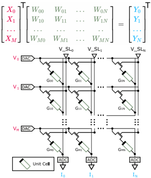
## Diagram: Analog-to-Digital Converter (ADC) Architecture
### Overview
The image depicts a schematic diagram of an array-based analog-to-digital converter (ADC) architecture. It combines a matrix multiplication operation with a resistive network to perform the conversion. The diagram shows input voltages (V0 to VM) being applied to a network of resistors (represented by G00 to GMN) and then converted to currents (I0 to IN) using ADCs. A matrix equation at the top represents the mathematical operation performed by the circuit.
### Components/Axes
The diagram consists of the following key components:
* **Matrix Equation:** A matrix equation at the top of the diagram representing the conversion process.
* **Input Voltages (V0 to VM):** Represented by horizontal lines labeled V0, V1, ..., VM.
* **Digital-to-Analog Converters (DACs):** Labeled "DAC" connected to each input voltage line.
* **Resistive Network (G00 to GMN):** Represented by rectangular resistors arranged in a grid. Labels indicate the resistance values (e.g., G00, G01, G10, G11, etc.).
* **Output Voltages (V_SL0 to V_SLN):** Represented by vertical lines labeled V_SL0, V_SL1, ..., V_SLN.
* **Analog-to-Digital Converters (ADCs):** Labeled "ADC" connected to each output current line.
* **Output Currents (I0 to IN):** Represented by lines labeled I0, I1, ..., IN.
* **Unit Cell:** A small rectangle in the bottom-left corner, labeled "Unit Cell", indicating the basic building block of the resistive network.
### Detailed Analysis / Content Details
The matrix equation at the top can be transcribed as:
```
[X₀] [W₀₀ W₀₁ ... W₀N] [Y₀]
[X₁] [W₁₀ W₁₁ ... W₁N] = [Y₁]
... [... ... ... ...] [...]
[Xₘ] [Wₘ₀ Wₘ₁ ... WₘN] [Yₙ]
```
Where:
* **X₀ to Xₘ** are the input vectors.
* **W₀₀ to WₘN** are the weighting coefficients (representing the resistance values).
* **Y₀ to Yₙ** are the output vectors.
The resistive network is arranged in an M x N grid. The resistors are labeled as follows:
* **Rows:** G00, G01, ..., G0N (corresponding to input voltage V0)
* **Rows:** G10, G11, ..., G1N (corresponding to input voltage V1)
* **...**
* **Rows:** GM0, GM1, ..., GMN (corresponding to input voltage VM)
The input voltages V0 to VM are connected to DACs, which drive the currents through the resistive network. The output currents I0 to IN are then measured by ADCs. The output voltages V_SL0 to V_SLN are the nodes where the currents are summed.
### Key Observations
* The diagram illustrates a parallel ADC architecture where multiple ADCs operate simultaneously.
* The matrix multiplication is implemented using a resistive network.
* The "Unit Cell" suggests that the resistive network is composed of identical building blocks.
* The diagram does not provide specific values for the resistances or the number of ADCs (N).
### Interpretation
This diagram represents a novel ADC architecture that leverages a resistive network to perform a matrix multiplication operation. This approach allows for parallel conversion, potentially increasing the speed of the ADC. The use of a "Unit Cell" suggests a modular design, which could simplify fabrication and improve scalability. The matrix equation at the top provides a mathematical representation of the conversion process, highlighting the relationship between the input voltages, the weighting coefficients (resistances), and the output currents. The diagram suggests a trade-off between accuracy (determined by the precision of the resistors and ADCs) and speed (determined by the number of parallel ADCs). The absence of specific numerical values limits a deeper quantitative analysis, but the diagram clearly demonstrates the fundamental principles of this ADC architecture. The diagram is a conceptual illustration, and does not provide details on the specific implementation of the DACs and ADCs.