\n
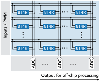
## Diagram: 8T4R System Architecture
### Overview
The image depicts a block diagram of an 8T4R (likely 8-Transmit, 4-Receive) system architecture. It illustrates the interconnection between input signals (Inputs/PWM) and output signals (Output for off-chip processing) via a matrix of 8T4R blocks and Analog-to-Digital Converters (ADCs). The diagram shows a repetitive structure, indicated by the ellipsis (...), suggesting a larger array of these components.
### Components/Axes
The diagram consists of the following key components:
* **8T4R Blocks:** Rectangular blocks labeled "8T4R". These appear to be the core processing elements.
* **Inputs/PWM:** A gray rectangular area labeled "Inputs / PWM" representing the input signals to the system.
* **ADCs:** Blocks labeled "ADC" representing Analog-to-Digital Converters.
* **Output for off-chip processing:** A label indicating the destination of the processed signals.
* **Interconnecting Lines:** Lines connecting the 8T4R blocks to both the input signals and the ADCs.
There are no explicit axes in this diagram. The arrangement is spatial, representing connections and flow.
### Detailed Analysis or Content Details
The diagram shows a matrix-like arrangement of 8T4R blocks.
* **Input Connections:** Each 8T4R block receives input from the "Inputs / PWM" section. Multiple input lines connect to each 8T4R block, suggesting parallel processing or multiple input channels.
* **8T4R Matrix:** The 8T4R blocks are arranged in rows and columns. The ellipsis (...) indicates that the matrix extends beyond what is visible in the diagram.
* **ADC Connections:** Each column of 8T4R blocks is connected to a single ADC. This suggests that the ADCs are responsible for converting the output of each column into a digital signal.
* **Output:** The output of the ADCs is labeled "Output for off-chip processing," indicating that the digital signals are sent to an external processing unit.
The diagram does not provide specific numerical values or parameters for the 8T4R blocks or ADCs. It is a high-level architectural representation.
### Key Observations
* **Parallel Processing:** The arrangement of 8T4R blocks and ADCs suggests a parallel processing architecture, where multiple input signals are processed simultaneously.
* **Matrix Structure:** The matrix-like arrangement of 8T4R blocks allows for flexible signal routing and processing.
* **Modular Design:** The repetitive structure of the diagram suggests a modular design, where the system can be easily scaled by adding more 8T4R blocks and ADCs.
### Interpretation
This diagram illustrates a system architecture commonly used in wireless communication or signal processing applications. The 8T4R blocks likely perform some form of signal amplification, filtering, or modulation. The ADCs convert the analog output of the 8T4R blocks into digital signals for further processing. The "Output for off-chip processing" suggests that the system is part of a larger system, where the processed signals are sent to an external processor for tasks such as decoding, error correction, or control.
The use of 8 transmit and 4 receive elements suggests a Multiple-Input Multiple-Output (MIMO) system, which is used to improve the capacity and reliability of wireless communication links. The diagram highlights the key components and their interconnections, providing a clear understanding of the system's overall architecture. The ellipsis indicates that the system can be scaled to accommodate a larger number of input and output channels. The diagram does not provide details about the specific functionality of the 8T4R blocks or ADCs, but it provides a valuable overview of the system's overall structure.