## Charts: Device Conductance Models (Write, Read, Drift)
### Overview
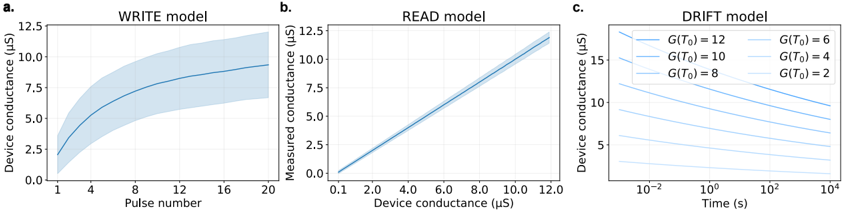
The image presents three separate charts illustrating different models related to device conductance: a "WRITE" model, a "READ" model, and a "DRIFT" model. Each chart depicts the relationship between conductance and another variable (pulse number, device conductance, and time, respectively). The charts use line plots with shaded areas to represent variability or confidence intervals.
### Components/Axes
**Chart a (WRITE model):**
* **Title:** WRITE model
* **X-axis:** Pulse Number (scale from 0 to 20, approximately)
* **Y-axis:** Device conductance (µS) (scale from 0 to 12.5 µS, approximately)
**Chart b (READ model):**
* **Title:** READ model
* **X-axis:** Device conductance (µS) (scale from 0.1 to 12.0 µS, approximately)
* **Y-axis:** Measured conductance (µS) (scale from 0 to 12.5 µS, approximately)
**Chart c (DRIFT model):**
* **Title:** DRIFT model
* **X-axis:** Time (s) (logarithmic scale, from 10<sup>-2</sup> to 10<sup>4</sup> s, approximately)
* **Y-axis:** Device conductance (µS) (scale from 0 to 16 µS, approximately)
* **Legend:**
* G(T<sub>0</sub>) = 12 (Dark Blue)
* G(T<sub>0</sub>) = 10 (Medium Blue)
* G(T<sub>0</sub>) = 8 (Light Blue)
* G(T<sub>0</sub>) = 6 (Very Light Blue)
* G(T<sub>0</sub>) = 4 (Pale Blue)
* G(T<sub>0</sub>) = 2 (Very Pale Blue)
### Detailed Analysis or Content Details
**Chart a (WRITE model):**
The line representing the WRITE model slopes upward, indicating that device conductance increases with pulse number. The line starts near 0 µS at Pulse Number 0 and reaches approximately 10 µS at Pulse Number 20. A large shaded area surrounds the line, indicating significant variability in the conductance response.
* At Pulse Number 1: ~0.5 µS
* At Pulse Number 4: ~2.5 µS
* At Pulse Number 8: ~5 µS
* At Pulse Number 12: ~7.5 µS
* At Pulse Number 16: ~9 µS
* At Pulse Number 20: ~10 µS
**Chart b (READ model):**
The line in the READ model is nearly linear and slopes upward. It starts near 0 µS at Device Conductance 0.1 µS and reaches approximately 12.5 µS at Device Conductance 12 µS. The shaded area is relatively small, suggesting a more consistent relationship between measured and device conductance.
* At Device Conductance 2 µS: ~2 µS
* At Device Conductance 4 µS: ~4 µS
* At Device Conductance 6 µS: ~6 µS
* At Device Conductance 8 µS: ~8 µS
* At Device Conductance 10 µS: ~10 µS
* At Device Conductance 12 µS: ~12 µS
**Chart c (DRIFT model):**
This chart shows multiple curves, each representing a different initial conductance G(T<sub>0</sub>). All curves slope downward, indicating that device conductance decreases over time. The rate of decrease is faster at shorter time scales and slows down as time increases.
* **G(T<sub>0</sub>) = 12 (Dark Blue):** Starts at ~12 µS and decreases to ~5 µS at 10<sup>4</sup> s.
* **G(T<sub>0</sub>) = 10 (Medium Blue):** Starts at ~10 µS and decreases to ~4 µS at 10<sup>4</sup> s.
* **G(T<sub>0</sub>) = 8 (Light Blue):** Starts at ~8 µS and decreases to ~3 µS at 10<sup>4</sup> s.
* **G(T<sub>0</sub>) = 6 (Very Light Blue):** Starts at ~6 µS and decreases to ~2 µS at 10<sup>4</sup> s.
* **G(T<sub>0</sub>) = 4 (Pale Blue):** Starts at ~4 µS and decreases to ~1 µS at 10<sup>4</sup> s.
* **G(T<sub>0</sub>) = 2 (Very Pale Blue):** Starts at ~2 µS and decreases to ~0.5 µS at 10<sup>4</sup> s.
### Key Observations
* The WRITE model exhibits the most variability in conductance response.
* The READ model shows a strong linear relationship between device and measured conductance.
* The DRIFT model demonstrates that conductance decreases over time, with the initial conductance level influencing the rate of decay.
* The DRIFT model curves appear to asymptotically approach zero conductance as time increases.
### Interpretation
These charts likely represent a model for a memristive device or a similar non-volatile memory element. The WRITE model shows how the device conductance is programmed with successive pulses. The READ model demonstrates the ability to accurately measure the programmed conductance. The DRIFT model illustrates the retention characteristics of the device, showing how conductance degrades over time. The variability in the WRITE model suggests that the writing process is not perfectly controlled, while the linear READ model indicates a reliable measurement process. The DRIFT model is crucial for understanding the long-term stability of the device. The parameter G(T<sub>0</sub>) represents the initial conductance at time zero, and the different curves show how the conductance evolves from different starting points. The logarithmic time scale in the DRIFT model is common for analyzing decay processes. The decreasing conductance over time suggests a gradual loss of stored information, which is a critical factor in memory device design.