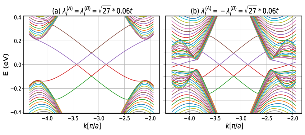
# Technical Data Extraction: Electronic Band Structure Plots
This document provides a detailed technical extraction of the data and visual information contained in the provided image, which consists of two side-by-side electronic band structure plots.
## 1. General Metadata and Global Axis
* **Image Type:** Scientific line plots (Band structure diagrams).
* **Y-Axis (Common):** Energy, labeled as **$E \text{ (eV)}$**.
* **Range:** $-0.4$ to $0.4$.
* **Major Tick Marks:** $-0.4, -0.2, 0.0, 0.2, 0.4$.
* **X-Axis (Common):** Wave vector, labeled as **$k [\pi/a]$**.
* **Range:** Approximately $-4.4$ to $-1.9$.
* **Major Tick Marks:** $-4.0, -3.5, -3.0, -2.5, -2.0$.
* **Grid:** Both plots feature a light gray rectangular grid aligned with the major tick marks.
---
## 2. Subplot (a) Analysis
**Header Label:** (a) $\lambda_I^{(A)} = \lambda_I^{(B)} = \sqrt{27} * 0.06t$
### Component Isolation & Trends
This plot shows a band structure with a clear energy gap and crossing states within that gap.
* **Bulk Bands (Top and Bottom):**
* **Conduction Bands (Top):** A dense manifold of parabolic-like curves starting around $E = 0.2 \text{ eV}$. They curve upward away from the center.
* **Valence Bands (Bottom):** A dense manifold of parabolic-like curves starting around $E = -0.2 \text{ eV}$. They curve downward away from the center.
* **Edge/Surface States (Crossing Lines):**
* There are four distinct linear bands that cross the band gap between $k = -4.0$ and $k = -2.0$.
* **Trend 1 (Positive Slope):** Two lines (one purple, one brown) slope upward from left to right. They cross $E = 0$ at approximately $k = -3.4$ and $k = -2.4$.
* **Trend 2 (Negative Slope):** Two lines (one red, one green) slope downward from left to right. They cross $E = 0$ at approximately $k = -3.4$ and $k = -2.4$.
* **Symmetry:** The plot is symmetric around the vertical line $k = -2.9$ (approximate center of the Brillouin zone shown).
---
## 3. Subplot (b) Analysis
**Header Label:** (b) $\lambda_I^{(A)} = -\lambda_I^{(B)} = \sqrt{27} * 0.06t$
### Component Isolation & Trends
This plot shows a significantly different topology compared to (a), characterized by a "pinched" or narrower gap and more complex oscillations in the bulk bands.
* **Bulk Bands (Top and Bottom):**
* The manifolds are much more spread out vertically compared to plot (a).
* **Oscillatory Behavior:** Near the gap edges (around $k = -4.0$ and $k = -2.3$), the bands exhibit "wavy" or oscillatory behavior rather than smooth parabolas.
* **Edge/Surface States (Crossing Lines):**
* Similar to (a), there are crossing linear bands in the center.
* **Trend 1 (Positive Slope):** A purple line and a brown line slope upward.
* **Trend 2 (Negative Slope):** A red line and a green line slope downward.
* **Key Difference:** The crossing points at $E = 0$ appear more compressed toward the center compared to plot (a). The "gap" between the bulk manifolds is narrower at the $k$ values where the edge states emerge.
* **Gap Structure:** The energy gap between the dense conduction and valence manifolds is significantly smaller in the regions between $k = -3.5$ and $k = -2.5$ compared to plot (a).
---
## 4. Comparative Summary
| Feature | Plot (a) | Plot (b) |
| :--- | :--- | :--- |
| **Parameter Relation** | $\lambda_I^{(A)} = \lambda_I^{(B)}$ | $\lambda_I^{(A)} = -\lambda_I^{(B)}$ |
| **Bulk Band Shape** | Smooth, parabolic manifolds. | Oscillatory/wavy manifolds near the gap. |
| **Energy Gap** | Wide and well-defined. | Narrower, with bulk states extending closer to $E=0$. |
| **Crossing States** | Clear linear crossings through a large vacuum. | Crossings exist but are surrounded by more complex bulk structures. |
**Technical Note:** These plots likely represent the band structure of a topological insulator or a similar 2D material (like a transition metal dichalcogenide or functionalized graphene) where $\lambda_I$ represents an intrinsic spin-orbit coupling parameter. The transition from (a) to (b) demonstrates how the relative sign of the coupling on different sublattices (A and B) alters the topological protection and the dispersion of the edge states.