TECHNICAL ASSET FINGERPRINT
e8e15f8d97de2f837c6a9717
Click to view fullscreen
Press ESC or click to close
FOUND IN PAPERS
EXPERT: gemini-2.0-flash VERSION 1
RUNTIME: nugit/gemini/gemini-2.0-flash
INTEL_VERIFIED
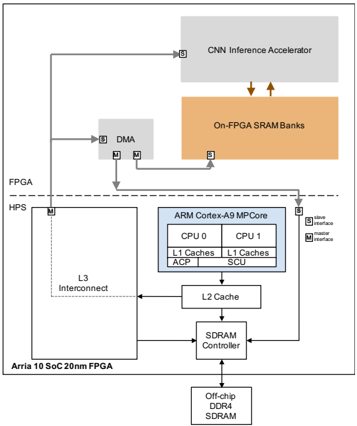
## System Diagram: Arria 10 SoC FPGA Architecture
### Overview
The image is a system diagram illustrating the architecture of an Arria 10 SoC (System on Chip) 20nm FPGA. It depicts the interconnection of various components, including a CNN Inference Accelerator, On-FPGA SRAM Banks, DMA (Direct Memory Access), an ARM Cortex-A9 MPCore, L3 Interconnect, L2 Cache, SDRAM Controller, and Off-chip DDR4 SDRAM. The diagram highlights the data flow and interfaces between these components within the FPGA and HPS (Hard Processor System) domains.
### Components/Axes
* **FPGA:** Field Programmable Gate Array section of the SoC.
* **HPS:** Hard Processor System section of the SoC.
* **CNN Inference Accelerator:** A block for accelerating Convolutional Neural Network inference.
* **On-FPGA SRAM Banks:** On-chip Static Random-Access Memory.
* **DMA:** Direct Memory Access controller.
* **ARM Cortex-A9 MPCore:** A multi-core ARM processor. Contains:
* CPU 0
* CPU 1
* L1 Caches (for both CPUs)
* ACP (Accelerator Coherency Port)
* SCU (Snoop Control Unit)
* **L3 Interconnect:** Interconnect fabric for the HPS.
* **L2 Cache:** Level 2 cache memory.
* **SDRAM Controller:** Controller for external SDRAM.
* **Off-chip DDR4 SDRAM:** External Dynamic Random-Access Memory.
* **Arria 10 SoC 20nm FPGA:** Label for the overall chip.
* **Slave Interface (S):** Denoted by the letter 'S' in a square.
* **Master Interface (M):** Denoted by the letter 'M' in a square.
### Detailed Analysis
* **CNN Inference Accelerator:** Located at the top of the diagram, within the FPGA domain. It has a slave interface.
* **On-FPGA SRAM Banks:** Located below the CNN Inference Accelerator, within the FPGA domain. It has a slave interface. Data flows between the CNN Inference Accelerator and the On-FPGA SRAM Banks, indicated by two downward-pointing arrows.
* **DMA:** Located to the left of the On-FPGA SRAM Banks, within the FPGA domain. It has both slave and master interfaces.
* **FPGA/HPS Boundary:** A dashed line separates the FPGA and HPS domains.
* **ARM Cortex-A9 MPCore:** Located within the HPS domain. It has a slave interface.
* **CPU 0 and CPU 1:** Each CPU has its own L1 Cache.
* **ACP and SCU:** Are also components within the ARM Cortex-A9 MPCore.
* **L3 Interconnect:** Located to the left of the ARM Cortex-A9 MPCore, within the HPS domain. It has a master interface.
* **L2 Cache:** Located below the ARM Cortex-A9 MPCore.
* **SDRAM Controller:** Located below the L2 Cache.
* **Off-chip DDR4 SDRAM:** Located at the bottom of the diagram.
* **Data Flow:**
* The CNN Inference Accelerator connects to the DMA via a line.
* The DMA connects to the On-FPGA SRAM Banks via two lines.
* The L3 Interconnect connects to the SDRAM Controller.
* The L2 Cache connects to the L3 Interconnect and the SDRAM Controller.
* The SDRAM Controller connects to the Off-chip DDR4 SDRAM.
### Key Observations
* The diagram illustrates a typical data processing pipeline, where the CNN Inference Accelerator processes data stored in the On-FPGA SRAM Banks.
* The DMA facilitates data transfer between the CNN Inference Accelerator and the On-FPGA SRAM Banks.
* The ARM Cortex-A9 MPCore interacts with the L2 Cache and SDRAM Controller to access external memory.
* The FPGA and HPS domains are clearly separated, indicating the partitioning of functionality between the programmable logic and the hard processor system.
### Interpretation
The diagram provides a high-level overview of the Arria 10 SoC FPGA architecture, emphasizing the data flow and interconnection of key components. It highlights the integration of a CNN Inference Accelerator, which suggests the device is designed for applications involving machine learning and image processing. The presence of both on-chip SRAM and off-chip DDR4 SDRAM indicates a memory hierarchy optimized for performance and capacity. The separation of the FPGA and HPS domains allows for flexible hardware acceleration and software control. The master and slave interfaces indicate the direction of data flow and control between the different components. Overall, the architecture is designed to support a wide range of embedded applications requiring high performance and low power consumption.
DECODING INTELLIGENCE...
EXPERT: gemma-3-27b-it-free VERSION 1
RUNTIME: google-free/gemma-3-27b-it
INTEL_VERIFIED
\n
## Diagram: FPGA System Architecture with CNN Inference Accelerator
### Overview
The image depicts a block diagram illustrating the architecture of an FPGA (Field-Programmable Gate Array) system, specifically an Arria 10 SoC 20nm FPGA, integrated with a CNN (Convolutional Neural Network) Inference Accelerator. The diagram showcases the data flow and interconnections between various components, including the FPGA HPS (Hard Processor System), ARM Cortex-A9 MPCore, memory components, and the CNN accelerator.
### Components/Axes
The diagram is composed of several key components:
* **FPGA HPS:** Located on the left side of the diagram, labeled "FPGA HPS".
* **Arria 10 SoC 20nm FPGA:** Located below the "FPGA HPS" label.
* **L3 Interconnect:** Connects the FPGA HPS to other components.
* **ARM Cortex-A9 MPCore:** A dual-core processor with CPU 0 and CPU 1, each having L1 Caches (ACP and SCU).
* **L2 Cache:** Connected to the ARM Cortex-A9 MPCore.
* **SDRAM Controller:** Connected to the L2 Cache.
* **Off-chip DDR4 SDRAM:** Memory connected to the SDRAM Controller.
* **DMA:** Direct Memory Access controller.
* **CNN Inference Accelerator:** Located at the top of the diagram.
* **On-FPGA SRAM Banks:** Memory connected to the CNN Inference Accelerator.
* **Interfaces:** Marked with "M" (Master) and "S" (Slave) labels, indicating the interface type.
* **Data Flow Arrows:** Indicate the direction of data transfer between components.
### Detailed Analysis or Content Details
The diagram illustrates the following data flow:
1. Data flows from the FPGA HPS through the L3 Interconnect to the ARM Cortex-A9 MPCore.
2. Within the ARM Cortex-A9 MPCore, data is processed by CPU 0 and CPU 1, utilizing their respective L1 Caches (ACP and SCU).
3. Data is then passed to the L2 Cache and subsequently to the SDRAM Controller.
4. The SDRAM Controller manages access to the Off-chip DDR4 SDRAM.
5. Data also flows from the FPGA HPS to the DMA controller.
6. The DMA controller transfers data to the CNN Inference Accelerator.
7. The CNN Inference Accelerator utilizes On-FPGA SRAM Banks for data storage and processing.
8. The CNN Inference Accelerator has a slave interface to the ARM Cortex-A9 MPCore.
9. The FPGA HPS has a master interface to the ARM Cortex-A9 MPCore.
The interfaces are labeled as follows:
* The connection between the FPGA HPS and the ARM Cortex-A9 MPCore is labeled with both "M" (Master) and "S" (Slave) interfaces.
* The connection between the CNN Inference Accelerator and the ARM Cortex-A9 MPCore is labeled with a "S" (Slave) interface.
* The connection between the DMA and the FPGA HPS is labeled with "M" (Master) and "S" (Slave) interfaces.
### Key Observations
The diagram highlights the integration of a dedicated CNN Inference Accelerator within an FPGA system. This suggests an architecture optimized for accelerating CNN-based applications. The use of both on-chip (SRAM Banks) and off-chip (DDR4 SDRAM) memory indicates a hierarchical memory system designed to balance speed and capacity. The presence of DMA suggests efficient data transfer mechanisms. The dual-core ARM processor provides general-purpose processing capabilities alongside the specialized CNN accelerator.
### Interpretation
This diagram represents a heterogeneous computing architecture. The FPGA provides a flexible platform for implementing custom hardware accelerators like the CNN Inference Accelerator. The ARM Cortex-A9 MPCore handles control and general-purpose tasks, while the CNN accelerator offloads computationally intensive CNN operations. The DMA controller facilitates efficient data transfer between the FPGA HPS, the CNN accelerator, and the memory system. The architecture is designed to achieve high performance and energy efficiency for CNN-based applications by leveraging the strengths of both hardware and software components. The use of both on-FPGA SRAM and off-chip DDR4 SDRAM suggests a strategy to optimize memory access patterns for the CNN accelerator, utilizing fast on-chip memory for frequently accessed data and larger off-chip memory for storing the entire model and datasets. The master/slave interface designations indicate the control flow and data access permissions between the different components. The diagram suggests a system where the FPGA HPS initiates data transfers and controls the overall operation, while the CNN accelerator operates as a co-processor.
DECODING INTELLIGENCE...
EXPERT: healer-alpha-free VERSION 1
RUNTIME: free/openrouter/healer-alpha
INTEL_VERIFIED
## System Architecture Diagram: Arria 10 SoC FPGA with HPS and CNN Accelerator
### Overview
This image is a technical block diagram illustrating the system architecture of an Intel/Altera Arria 10 System-on-Chip (SoC) Field-Programmable Gate Array (FPGA). The diagram is divided into two primary domains separated by a horizontal dashed line: the **FPGA** fabric (top) and the **Hard Processor System (HPS)** (bottom). It details the components, memory hierarchy, and data flow pathways for a system designed to accelerate Convolutional Neural Network (CNN) inference.
### Components/Axes
The diagram is a component and interconnect map, not a chart with axes. The key elements are:
**1. Primary Domains:**
* **FPGA:** The programmable logic region, occupying the top half of the diagram.
* **HPS (Hard Processor System):** The fixed, hardwired processor region, occupying the bottom half. A label in the bottom-left corner identifies the specific device: **"Arria 10 SoC 20nm FPGA"**.
**2. Major Functional Blocks:**
* **CNN Inference Accelerator:** A large grey block in the top-center of the FPGA region.
* **On-FPGA SRAM Banks:** A large orange block directly below the CNN Accelerator within the FPGA.
* **DMA (Direct Memory Access):** A smaller grey block to the left of the CNN Accelerator within the FPGA.
* **ARM Cortex-A9 MPCore:** A blue-outlined block in the HPS region. It contains:
* **CPU 0** and **CPU 1**
* **L1 Caches** (for each CPU)
* **ACP** (Accelerator Coherency Port)
* **SCU** (Snoop Control Unit)
* **L2 Cache:** A block below the ARM Core in the HPS.
* **L3 Interconnect:** A large block to the left of the ARM Core/L2 Cache in the HPS.
* **SDRAM Controller:** A block below the L2 Cache in the HPS.
* **Off-chip DDR4 SDRAM:** A block at the very bottom of the diagram, connected to the SDRAM Controller.
**3. Legend (Position: Center-Right):**
A small box defines the arrow types:
* **Solid Arrow:** Labeled **"Memory Access"**.
* **Dashed Arrow:** Labeled **"Configuration Access"**.
### Detailed Analysis
**Component Isolation & Spatial Grounding:**
* **FPGA Region (Top):**
* The **CNN Inference Accelerator** (top-center) has a bidirectional solid arrow (Memory Access) connecting it to the **On-FPGA SRAM Banks** (directly below it).
* The **DMA** (left of CNN Accelerator) has:
* A bidirectional solid arrow to the **On-FPGA SRAM Banks**.
* A bidirectional solid arrow crossing the dashed line to the **HPS** region (specifically connecting to the L3 Interconnect/SDRAM path).
* A dashed arrow (Configuration Access) pointing from the **HPS** (specifically from the ARM Core area) to the DMA.
* **HPS Region (Bottom):**
* The **ARM Cortex-A9 MPCore** (center-right of HPS) has:
* A solid arrow pointing down to the **L2 Cache**.
* A bidirectional solid arrow connecting to the **L3 Interconnect** (to its left).
* A dashed arrow (Configuration Access) pointing up, crossing the dashed line to the **DMA** in the FPGA.
* The **L2 Cache** connects via a solid arrow down to the **SDRAM Controller**.
* The **L3 Interconnect** has a solid arrow pointing right to the **SDRAM Controller**.
* The **SDRAM Controller** has a solid arrow pointing down to the **Off-chip DDR4 SDRAM**.
**Data Flow Pathways (Trend Verification):**
The primary data movement trends are:
1. **Accelerator Data Path:** Data likely flows from Off-chip SDRAM -> SDRAM Controller -> L3 Interconnect -> DMA -> On-FPGA SRAM Banks -> CNN Inference Accelerator for processing. Results may flow back via the reverse path.
2. **Processor Control Path:** The ARM Core configures the DMA (via Configuration Access) and manages the overall system. It accesses main memory (DDR4) through the L2 Cache and SDRAM Controller.
3. **Coherency Path:** The ACP port on the ARM Core suggests a mechanism to maintain cache coherency between the processor and the FPGA-based accelerator.
### Key Observations
1. **Hierarchical Memory:** The design features a clear memory hierarchy: Off-chip DDR4 (large, slow) -> On-FPGA SRAM (smaller, fast, local to accelerator) -> L2/L1 Caches (processor-local).
2. **Accelerator Isolation:** The CNN Accelerator is physically located in the FPGA fabric but is tightly coupled to dedicated on-chip SRAM for high-bandwidth, low-latency access during inference.
3. **DMA as Bridge:** The DMA controller is the critical bridge between the high-performance FPGA accelerator domain and the general-purpose HPS domain, handling bulk data transfers.
4. **Tight Integration:** The diagram emphasizes the "System-on-Chip" nature, showing the hardwired ARM processors (HPS) and programmable logic (FPGA) on a single die with high-bandwidth interconnects (L3 Interconnect, SDRAM Controller).
5. **Asymmetric Connection:** The connection from the FPGA (DMA) to the HPS is a single, bidirectional memory access path, while the HPS has configuration access *to* the FPGA components.
### Interpretation
This diagram illustrates a **heterogeneous computing architecture** optimized for edge AI inference. The design philosophy is to offload the computationally intensive, parallelizable task of CNN inference to a dedicated hardware accelerator in the FPGA fabric, while leaving general-purpose control, pre/post-processing, and system management to the ARM Cortex-A9 processors.
* **What it demonstrates:** It shows a practical implementation for achieving high performance and power efficiency in AI applications. The FPGA provides reconfigurable hardware acceleration, the on-FPGA SRAM eliminates the memory bandwidth bottleneck for the accelerator, and the integrated HPS allows for a complete, standalone system without needing a separate host CPU.
* **Relationships:** The components form a pipeline. The HPS acts as the master, orchestrating operations and configuring the accelerator via the DMA. The DMA shuttles input data and results between the main system memory (DDR4) and the accelerator's local memory (SRAM). The CNN Accelerator performs the core computation.
* **Notable Anomaly/Design Choice:** The use of **DDR4** (instead of DDR3) suggests this is a relatively modern or performance-oriented design, as Arria 10 FPGAs support both. The specific choice of a dual-core **Cortex-A9** (an older ARM core) indicates this may be a cost-optimized or legacy-compatible SoC variant, balancing processing power with the advanced FPGA fabric. The entire system is built on a **20nm process**, which was cutting-edge at its introduction, enabling high logic density and performance.
DECODING INTELLIGENCE...
EXPERT: nemotron-free VERSION 1
RUNTIME: free/nvidia/nemotron-nano-12b-v2-vl:free
INTEL_VERIFIED
## Diagram: CNN Inference Accelerator Architecture
### Overview
The diagram illustrates a heterogeneous computing system architecture for CNN inference acceleration. It integrates FPGA, ARM Cortex-A9 MPCore, DDR4 SDRAM, and On-FPGA SRAM Banks, with data flow managed via L3 Interconnect, DMA, and master/slave interfaces.
### Components/Axes
- **Key Components**:
- **FPGA**: Arria 10 SoC 20nm FPGA (left side).
- **HPS**: Connected to FPGA via L3 Interconnect.
- **ARM Cortex-A9 MPCore**: Central block with dual CPUs (CPU0, CPU1), L1/L2 caches, ACP, SCU, and SDRAM Controller.
- **Off-chip DDR4 SDRAM**: Connected to SDRAM Controller.
- **CNN Inference Accelerator**: Top-right block, linked to On-FPGA SRAM Banks.
- **On-FPGA SRAM Banks**: Orange block, directly connected to CNN Inference Accelerator.
- **DMA**: Gray block, bridges FPGA and ARM Cortex-A9 MPCore.
- **Data Flow**:
- Arrows indicate bidirectional communication (e.g., FPGA ↔ HPS, ARM ↔ DDR4 SDRAM).
- Master/slave interfaces (labeled "M" and "S") define communication roles.
### Detailed Analysis
- **FPGA and HPS**:
- FPGA (Arria 10 SoC 20nm) connects to HPS via L3 Interconnect.
- DMA mediates data transfer between FPGA and ARM Cortex-A9 MPCore.
- **ARM Cortex-A9 MPCore**:
- Dual CPUs (CPU0, CPU1) with shared L1 caches.
- ACP (Advanced Communication Peripheral) and SCU (System Control Unit) manage system-level tasks.
- L2 Cache sits between CPUs and SDRAM Controller.
- **Memory Hierarchy**:
- Off-chip DDR4 SDRAM is the primary memory, controlled by the SDRAM Controller.
- On-FPGA SRAM Banks provide low-latency access for the CNN Inference Accelerator.
- **CNN Inference Accelerator**:
- Directly connected to On-FPGA SRAM Banks, suggesting optimized data throughput for inference tasks.
### Key Observations
1. **Hierarchical Design**:
- FPGA and HPS handle peripheral/data acquisition, while ARM Cortex-A9 MPCore manages general computation.
- CNN Inference Accelerator offloads specialized tasks to On-FPGA SRAM for speed.
2. **Memory Optimization**:
- On-FPGA SRAM Banks reduce latency for the CNN accelerator compared to off-chip DDR4 SDRAM.
- L3 Interconnect and DMA enable efficient data sharing between FPGA and ARM cores.
3. **Interface Roles**:
- Master/slave labels ("M" and "S") clarify communication directionality (e.g., FPGA as master to HPS).
### Interpretation
This architecture prioritizes **performance isolation** and **data locality**:
- The CNN Inference Accelerator leverages On-FPGA SRAM for rapid access, critical for low-latency inference.
- ARM Cortex-A9 MPCore handles general-purpose tasks, offloading compute-heavy CNN work to the FPGA.
- The use of DMA and L3 Interconnect minimizes CPU overhead for data transfers, improving scalability.
The design reflects a **coarse-grained parallelism** approach, where specialized hardware (FPGA accelerator) and general-purpose cores (ARM) collaborate via optimized memory and interconnects. The absence of explicit numerical values suggests a focus on architectural relationships rather than quantitative benchmarks.
DECODING INTELLIGENCE...