TECHNICAL ASSET FINGERPRINT
ee01de769247fc96589ecead
Click to view fullscreen
Press ESC or click to close
FOUND IN PAPERS
EXPERT: healer-alpha-free VERSION 1
RUNTIME: free/openrouter/healer-alpha
INTEL_VERIFIED
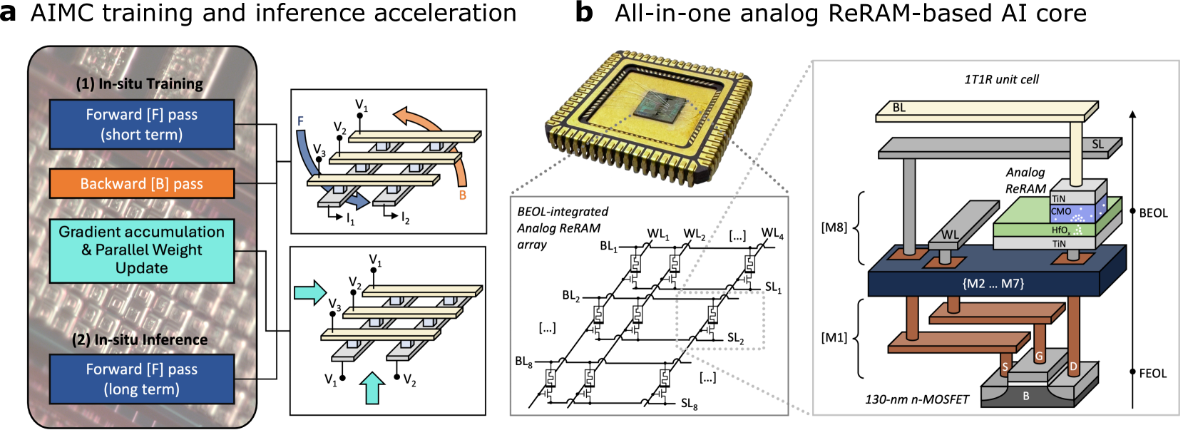
## Technical Diagram: AIMC Training/Inference Acceleration & Analog ReRAM AI Core
### Overview
The image is a composite technical diagram divided into two main panels, labeled **a** and **b**. Panel **a** illustrates the conceptual flow of Analog In-Memory Computing (AIMC) for training and inference acceleration. Panel **b** details the physical implementation of an "All-in-one analog ReRAM-based AI core," showing the chip, its memory array structure, and a detailed cross-section of a single memory cell.
### Components/Axes
The diagram contains no traditional chart axes. It is composed of labeled blocks, circuit schematics, and illustrative diagrams.
**Panel a: AIMC training and inference acceleration**
* **Main Block (Left):** A rounded rectangle with a background image of a circuit board. It contains two sub-sections:
* **(1) In-situ Training:** Contains three colored blocks:
* Blue: "Forward [F] pass (short term)"
* Orange: "Backward [B] pass"
* Teal: "Gradient accumulation & Parallel Weight Update"
* **(2) In-situ Inference:** Contains one blue block:
* "Forward [F] pass (long term)"
* **Circuit Diagrams (Right):** Two schematic diagrams connected by lines to the main block, illustrating the electrical operation.
* **Top Diagram:** Shows a crossbar array with word lines (V1, V2, V3) and bit lines (I1, I2). Arrows labeled **F** (blue, curved) and **B** (orange, curved) indicate forward and backward pass current flows.
* **Bottom Diagram:** Shows a similar crossbar array. A large teal arrow points right, and a smaller teal arrow points up, indicating the direction of weight update operations.
**Panel b: All-in-one analog ReRAM-based AI core**
* **Chip Photo (Top-Left):** A photograph of a packaged integrated circuit (IC) with a central die.
* **Array Diagram (Bottom-Left):** A schematic labeled "BEOL-integrated Analog ReRAM array." It shows a grid of 1T1R (one transistor, one resistor) cells.
* **Horizontal Lines:** Labeled as Word Lines: `WL1`, `WL2`, `...`, `WL4`.
* **Vertical Lines:** Labeled as Bit Lines (`BL1`, `BL2`, `...`, `BL8`) and Source Lines (`SL1`, `SL2`, `...`, `SL8`).
* **Unit Cell Cross-Section (Right):** A detailed 3D diagram labeled "1T1R unit cell." It shows the vertical stack of materials and layers.
* **Top Layers (BEOL - Back End Of Line):** From top to bottom:
* `BL` (Bit Line)
* `SL` (Source Line)
* `WL` (Word Line)
* **Analog ReRAM stack:** Labeled layers are `TiN` (top electrode), `CMO` (likely a conductive metal oxide), `HfO₂` (hafnium dioxide switching layer), `TiN` (bottom electrode).
* **Bottom Layers (FEOL - Front End Of Line):**
* `{M2 ... M7}`: Represents intermediate metal layers.
* `[M1]`: First metal layer.
* **Transistor:** A `130-nm n-MOSFET` with terminals labeled `S` (Source), `G` (Gate), `D` (Drain), and `B` (Body/Bulk).
* **Vertical Axis:** An arrow on the right side indicates the vertical progression from FEOL at the bottom to BEOL at the top.
### Detailed Analysis
**Panel a - Conceptual Flow:**
1. **In-situ Training Process:** The diagram outlines a three-step training cycle performed directly within the analog memory array:
* Step 1: A short-term **Forward [F] pass**.
* Step 2: A **Backward [B] pass** for error propagation.
* Step 3: **Gradient accumulation & Parallel Weight Update**, where weight adjustments are applied simultaneously across the array.
2. **In-situ Inference Process:** A separate, simpler process for using the trained model:
* A long-term **Forward [F] pass** for executing inference tasks.
3. **Circuit Operation:** The accompanying schematics visually map these algorithmic steps to physical current flows (`F`, `B`) and voltage/weight update operations (teal arrows) within the crossbar array hardware.
**Panel b - Hardware Implementation:**
1. **Physical Chip:** The top-left photo shows the final packaged product, the "AI core."
2. **Memory Array Architecture:** The bottom-left schematic details how the ReRAM cells are organized in a crossbar structure, addressed by word lines (`WL`) and read/written via bit lines (`BL`) and source lines (`SL`). The `[...]` notation indicates the array extends beyond the shown 4x8 segment.
3. **1T1R Unit Cell Structure:** The right-side cross-section reveals the nanoscale engineering:
* The resistive memory element (**Analog ReRAM**) is built in the **BEOL** layers, using a `TiN/CMO/HfO₂/TiN` material stack.
* This ReRAM element is connected in series with a selection transistor, a `130-nm n-MOSFET`, built in the **FEOL** silicon layer.
* The transistor's gate (`G`) is connected to a word line (`WL`), controlling access to the ReRAM cell. The ReRAM is connected between the bit line (`BL`) and source line (`SL`).
### Key Observations
1. **Tight Integration:** The diagram emphasizes the co-location of compute and memory ("In-situ"), which is the core principle of AIMC, aiming to overcome the von Neumann bottleneck.
2. **Dual-Purpose Hardware:** The same physical ReRAM array is used for both training and inference, with the training process being more complex (involving forward, backward, and update passes).
3. **Standard CMOS Integration:** The use of a `130-nm n-MOSFET` and standard BEOL/FEOL terminology indicates this is designed for integration with conventional silicon CMOS manufacturing processes.
4. **Analog Nature:** The ReRAM is explicitly labeled "Analog," meaning it stores weights as continuous conductance values, not discrete binary states, enabling efficient matrix-vector multiplication.
### Interpretation
This diagram illustrates a complete hardware-software co-design for an analog AI accelerator. Panel **a** defines the *what* and *how* of the computational algorithm—performing neural network training and inference directly within memory. Panel **b** reveals the *physical embodiment*—a specialized chip where the fundamental building block is a 1T1R cell that combines a non-volatile analog memory (ReRAM) with a standard transistor.
The key technical insight is the **vertical integration** shown in the 1T1R cell. By stacking the analog memory element (BEOL) directly on top of the selection transistor (FEOL), the design achieves high density and efficient electrical access. This architecture enables the parallel operations described in panel **a**, such as the "Parallel Weight Update," where many memory cells can be modified simultaneously by applying appropriate voltages to the word and bit lines.
The mention of "130-nm" suggests this is not a cutting-edge process node, implying the design may prioritize cost, reliability, or analog performance characteristics over sheer miniaturization. The overall system aims to dramatically accelerate AI workloads by performing the most computationally intensive operations (matrix multiplications for forward/backward passes) in the analog domain with minimal data movement.
DECODING INTELLIGENCE...