\n
## Diagram: L1 TCDM and IMA Architecture
### Overview
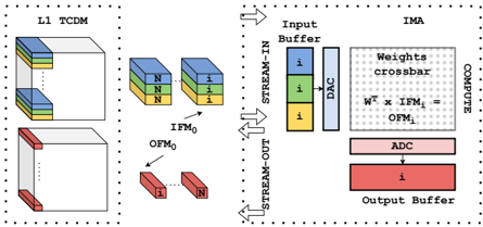
The image depicts a diagram illustrating the architecture of an L1 TCDM (Third-Order Correlation Detector Memory) and its interface with an IMA (In-Memory Accelerator). The diagram shows the data flow from the L1 TCDM to the IMA, highlighting the input buffering, weight crossbar, computation, and output buffering stages. The diagram uses color-coding to represent different data elements and stages.
### Components/Axes
The diagram is divided into two main sections: L1 TCDM (left) and IMA (right).
* **L1 TCDM:** Shows a 3D representation of memory blocks with colored layers. Labels include "L1 TCDM", "IFM₀", "OFM₀", and "i" and "N" within the blocks.
* **IMA:** Contains components labeled "Input Buffer", "Weights crossbar", "COMPUTE", "ADC", and "Output Buffer". Arrows indicate data flow labeled "STREAM-IN" and "STREAM-OUT".
* **Equation:** "Wᵀ x IFM₀ = OFM₀" is present within the "Weights crossbar" section.
* **Color Coding:**
* Blue: Represents input data "i".
* Yellow: Represents data "N".
* Red: Represents output data.
* Gray: Represents the structure of the memory blocks.
### Detailed Analysis or Content Details
**L1 TCDM:**
* The L1 TCDM shows a series of stacked blocks. The top block has layers colored blue, yellow, and blue. The bottom block has layers colored red.
* The label "IFM₀" points to the blue and yellow blocks, indicating the input feature map.
* The label "OFM₀" points to the red blocks, indicating the output feature map.
* The letters "i" and "N" are present within the blocks, likely representing data elements or indices.
**IMA:**
* **Input Buffer:** Contains three stacked blocks colored blue, labeled "i". A "DAC" (Digital-to-Analog Converter) is also present.
* **Weights Crossbar:** A grid-like structure labeled "Weights crossbar" is shown. The equation "Wᵀ x IFM₀ = OFM₀" is embedded within this section, indicating a matrix multiplication operation.
* **ADC:** An "ADC" (Analog-to-Digital Converter) is present after the "Weights crossbar".
* **Output Buffer:** Contains a single red block labeled "i".
**Data Flow:**
* "STREAM-IN" arrows point from the L1 TCDM to the Input Buffer.
* "STREAM-OUT" arrows point from the Output Buffer.
* The data flow within the IMA is sequential: Input Buffer -> Weights Crossbar -> ADC -> Output Buffer.
### Key Observations
* The diagram illustrates a data flow from the L1 TCDM to the IMA for performing a matrix multiplication operation.
* The use of color-coding helps to visualize the different data elements and stages of the process.
* The equation "Wᵀ x IFM₀ = OFM₀" highlights the core computation performed by the IMA.
* The diagram focuses on the architectural components and data flow rather than specific numerical values.
### Interpretation
The diagram demonstrates an architecture for accelerating computations by leveraging in-memory processing. The L1 TCDM serves as a memory block holding input and output feature maps (IFM₀ and OFM₀). The IMA performs a matrix multiplication (Wᵀ x IFM₀) using a weights crossbar, converting data between digital and analog domains using DAC and ADC, and storing the result in an output buffer. The STREAM-IN and STREAM-OUT arrows indicate the data transfer between the memory and the accelerator. This architecture aims to reduce data movement, which is a major bottleneck in traditional computing systems, by performing computations directly within the memory. The use of "i" and "N" within the memory blocks suggests indexing or data partitioning schemes. The diagram is a high-level representation of the system and does not provide details on the specific implementation of the components or the size of the data elements. It is a conceptual illustration of a potential hardware architecture for efficient machine learning or signal processing applications.