## Diagram: Chip Layout and Specifications
### Overview
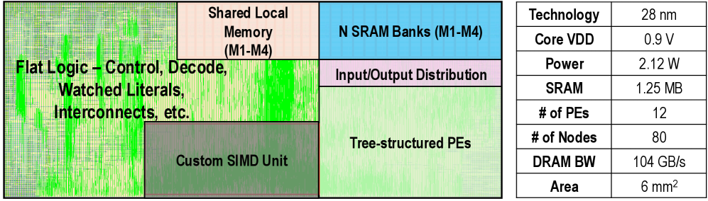
The image presents a high-level layout of a chip, alongside a table summarizing its key specifications. The chip layout diagram shows the functional blocks and their relative sizes, while the table provides numerical data on technology, power, memory, and performance characteristics.
### Components/Axes
**Chip Layout Diagram:**
* **Functional Blocks:** The diagram is divided into several colored rectangular blocks, each representing a different functional unit within the chip.
* **Flat Logic:** Located on the left side, labeled "Flat Logic - Control, Decode, Watched Literals, Interconnects, etc." (Light Yellow/Green)
* **Shared Local Memory:** Located at the top-center, labeled "Shared Local Memory (M1-M4)" (Light Peach)
* **N SRAM Banks:** Located at the top-right, labeled "N SRAM Banks (M1-M4)" (Light Blue)
* **Input/Output Distribution:** Located in the center-right, labeled "Input/Output Distribution" (Light Purple)
* **Tree-structured PEs:** Located at the bottom-right, labeled "Tree-structured PEs" (Light Green)
* **Custom SIMD Unit:** Located at the bottom-left, labeled "Custom SIMD Unit" (Darker Green)
**Specification Table:**
* **Rows:** Each row represents a different specification parameter.
* **Columns:** Two columns: Parameter Name and Value.
### Detailed Analysis or ### Content Details
**Chip Layout Diagram:**
* The "Flat Logic" block occupies a significant portion of the left side of the chip.
* The "Shared Local Memory" and "N SRAM Banks" are positioned at the top, suggesting their importance for data access.
* The "Input/Output Distribution" block is centrally located, facilitating communication between different units.
* The "Tree-structured PEs" and "Custom SIMD Unit" are at the bottom, indicating their role in processing.
**Specification Table:**
| Parameter | Value |
|-------------|----------|
| Technology | 28 nm |
| Core VDD | 0.9 V |
| Power | 2.12 W |
| SRAM | 1.25 MB |
| # of PEs | 12 |
| # of Nodes | 80 |
| DRAM BW | 104 GB/s |
| Area | 6 mm² |
### Key Observations
* The chip integrates various functional units, including logic, memory, and processing elements.
* The specification table provides quantitative data on the chip's performance and characteristics.
* The layout diagram gives a visual representation of the chip's architecture.
### Interpretation
The image provides a concise overview of a chip's design and performance. The layout diagram illustrates the physical arrangement of functional blocks, while the specification table quantifies key parameters such as technology node, power consumption, memory capacity, and processing capabilities. The combination of these two representations offers a comprehensive understanding of the chip's architecture and performance characteristics. The chip appears to be designed for parallel processing, given the presence of multiple processing elements (PEs) and a SIMD unit. The DRAM bandwidth is relatively high, suggesting a focus on memory-intensive applications.